
High-Precision Semiconductor Equipment Integration & Turnkey Wet Process Systems
KOSEN SEMI provides global semiconductor manufacturers with end-to-end engineering services, from custom wet bench solutions and hardware-software integration to ultra-pure cleanroom assembly.
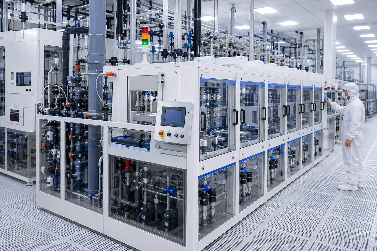
Core Integration Architecture and Modular Capabilities
KOSEN SEMI engineers high-reliability hardware platforms engineered for high-throughput semiconductor manufacturing. By combining custom wet bench layout configurations with modular equipment assembly and ultra-pure fluid integration, we deliver robust, scalable wet process tools engineered for demanding fab environments.
Modular Wet Bench Frame Assembly
Corrosion-resistant PFA and PVDF chemical baths integrate with precision multi-axis robotics to form a rigid, scalable equipment foundation. Learn more about our advanced Engineering Capability for customized semiconductor equipment designs.
- Corrosion-resistant PFA/PVDF bath integration
- Multi-axis robotics path synchronization
- Configurable frame footprint for fab layouts
Precision Fluid & Chemical Piping
Advanced IR fusion PFA welding and leak-resistant encapsulation support ultra-pure fluid integration across high-purity delivery loops for high-performance wafer-cleaning-systems.
- Infrared PFA fusion welding
- Ultra-high-purity microfluidic routing
- Secondary leak containment & sensor monitoring
Electrical Control & Safety Systems
Fully compliant with FM4910 fire safety standards, integrating explosion-proof chemical delivery and dual-circuit safety interlocks for our Single Wafer Cleaning Systems.
- FM4910 fire safety compliance
- Explosion-proof gas delivery & purge
- Dual-circuit hardware safety interlocks
Engineered for Rapid Customization and High Yields
Our modular equipment assembly framework enables tailored process configurations across clean, etch, and strip applications. KOSEN SEMI accelerates installation lead times while enforcing stringent ultra-pure fluid integration standards and structural safety protocols.
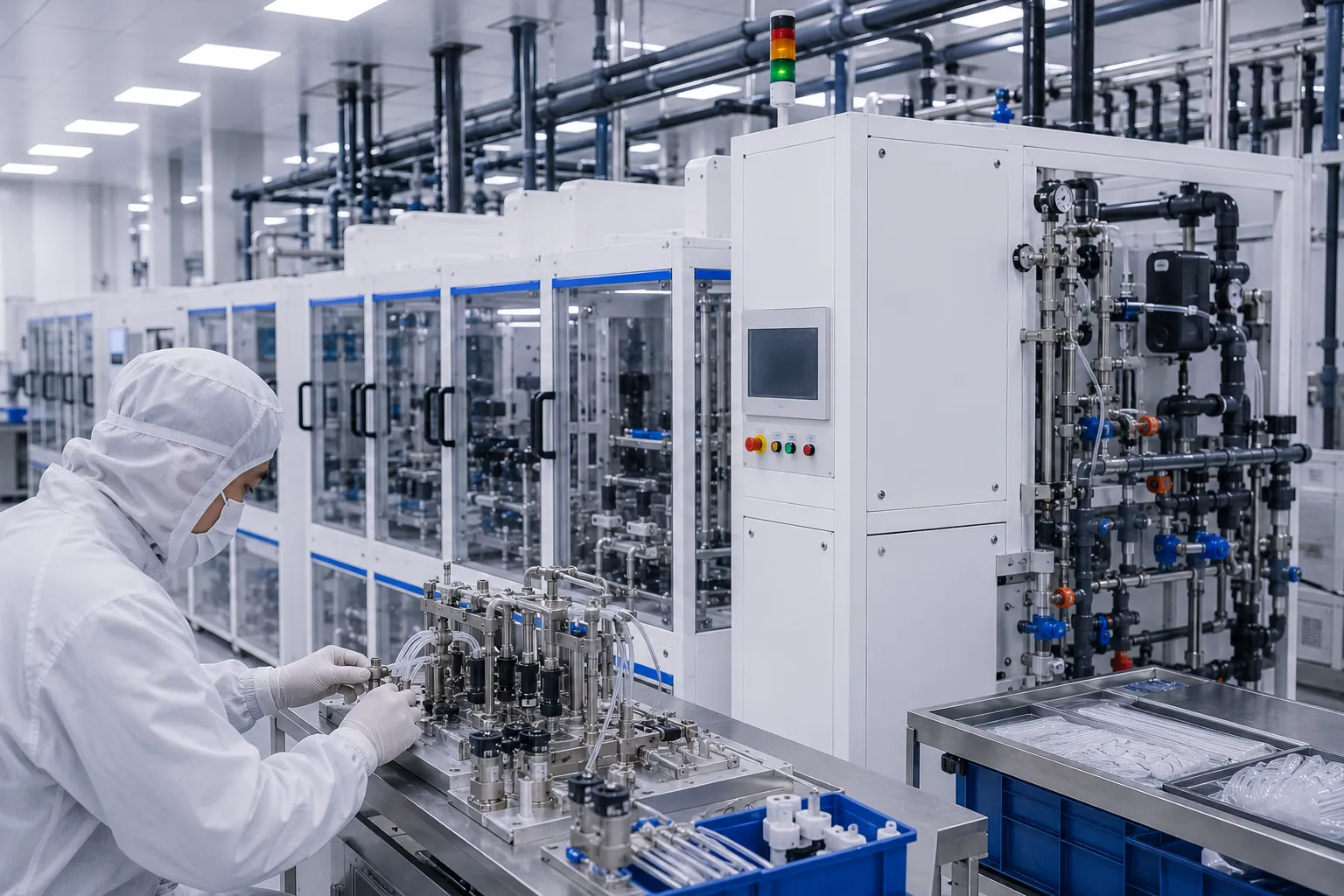
Connecting Hardware with Fab Central Control Systems (MES/EAP)
Equipment integration in advanced semiconductor manufacturing requires far more than physical assembly and precision chemical plumbing. At modern fabrication facilities, our engineering team maintains a primary focus on seamless factory automation integration. KOSEN SEMI bridges the gap between hardware execution and high-level fab host architectures. Through native SECS/GEM interface implementation, high-speed HSMS communications, and intelligent PLC dispatching, our wet process control integration supports reliable wafer transport, precise recipe adherence, and stable chemical handling across complex manufacturing environments.
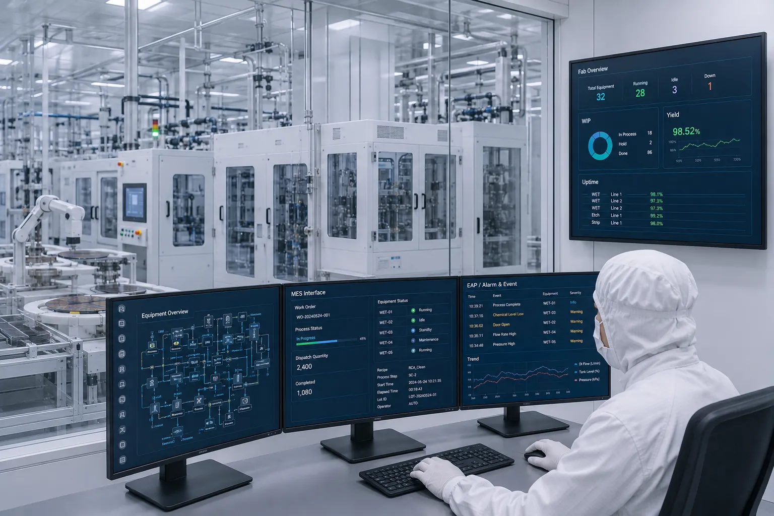
SECS/GEM and MES Communication Integration
Standardized communication protocols form the operational backbone of modern automated semiconductor fabrication lines. KOSEN SEMI's integrated software architecture natively supports applicable SEMI standard suites across wafer cleaning systems, reducing reliance on third-party middleware converters that may introduce network latency or potential handshake failures.
Key Communication Capabilities
- Native SECS/GEM Interface Architecture: Fully compliant with SEMI E4 (SECS-I), SEMI E5 (SECS-II), SEMI E30 (GEM), and SEMI E37 (HSMS) standards for reliable, bidirectional host-to-tool data transfer.
- Automated Carrier & Wafer Tracking: Real-time synchronization between the wet bench equipment controller and the Fab Host (MES/EAP) verifies recipe parameters, lot IDs, and process conditions prior to chemical immersion.
- Event-Driven Telemetry & Alarm Management: Dynamic S6F11 event reports and immediate S5F1 alarm notifications stream granular tool health telemetry directly into central control systems for proactive yield protection.
KOSEN SEMI's integrated software architecture seamlessly connects with major mainstream Fab automation systems, allowing semiconductor manufacturers to reduce equipment integration cycles by up to 40%.
Turnkey Cleanroom Integration & Semiconductor Equipment Testing
KOSEN SEMI delivers full-scope wet process integration engineered to reduce technical risks and accelerate production ramp-up. From initial 3D digital simulation and ISO Class 5–7 cleanroom assembly to rigorous FAT and SAT validation, our standardized turnkey workflow supports compliance with demanding semiconductor manufacturing standards.
Requirements Customization and 3D Layout Simulation
Comprehensive CAD engineering and 3D architectural modeling to optimize cleanroom footprint, chemical fluid paths, and sub-fab utility drops, showcasing our core Engineering Capability.
- •3D digital twin layout & kinematic modeling
- •Computational fluid dynamics (CFD) analysis
- •Sub-fab hookup & utility drop optimization
ISO Class 5–7 Cleanroom Assembly and Orbital Welding
High-purity mechanical assembly and ultra-clean fluid piping executed within controlled environments to minimize airborne particle risk.
- •Turnkey cleanroom integration & execution
- •Automated PFA and PVDF orbital welding
- •Ultra-high purity helium leak detection
Hardware-Software Interlock Tuning and SECS/GEM Testing
Integration of automated multi-axis transfer robotics, PLC controllers, and standard host communication protocols for fault-tolerant fab connection.
- •SECS/GEM interface protocol validation
- •Dual-circuit safety interlock setup
- •Closed-loop process control testing
Factory Acceptance Testing and Site Acceptance Testing
Structured multi-stage semiconductor equipment testing, spanning dry mechanical sequences, chemical trial runs, and final on-site fab commissioning.
- •Rigorous FAT SAT validation standards
- •Particle count & chemical purity verification
- •On-site line qualification & operator training
Rigorous Engineering Controls to Minimize Integration Risks
High-yield wafer fabrication requires total structural stability, precise chemical control, and strict contamination suppression. Learn more about us and how KOSEN SEMI manages every stage of custom wet bench engineering under a unified, ISO-certified quality management framework. By maintaining full internal control over structural fabrication, high-purity fluidic welding, and automation programming, we eliminate communication silos and significantly reduce project lead times.
Our specialized turnkey cleanroom integration protocols ensure that equipment arrives at your fab in plug-and-play condition, including our specialized Single Wafer Cleaning Systems. Prior to dispatch, every wet processing tool undergoes comprehensive semiconductor equipment testing to verify chemical dispense accuracy, pressure containment integrity, and automated fault-recovery behaviors under operational stress.
Controlled airborne particle contamination during high-purity fluid line routing.
Direct compatibility with central MES host control and automated dispatchers.
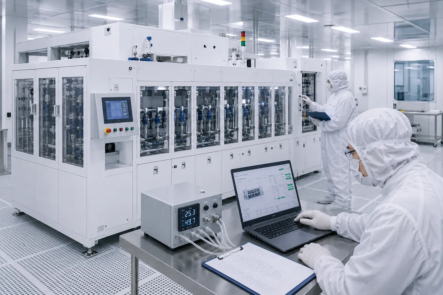
High-purity semiconductor wet bench undergoing comprehensive FAT validation inside our ISO Class 5–7 cleanroom integration facility.
Comprehensive Semiconductor Equipment Testing & Validation Milestones
To establish clear quality benchmarks throughout tool construction and deployment, KOSEN SEMI enforces structured verification milestones during assembly, factory testing, and final fab installation.
| Testing Phase | Engineering Scope | Validation Criteria | Customer Impact |
|---|---|---|---|
| Dry Run Pre-Testing | Robotic transfer kinematics, optical positioning sensors, and emergency stop interlocks | Sub-millimeter arm repeatability with minimized mechanical interference risk | Reduces mechanical errors prior to chemical introduction |
| Factory Acceptance (FAT) | DI water recirculation, precise acid/solvent dosing, temperature stability, and SECS/GEM logging | Flow rate variance below 1% with protocol alarm compliance verified during testing | Verifies all process specs before equipment leaves the factory floor |
| Site Acceptance (SAT) | Fab utility hookup checks, cleanroom particle verification, and process recipe tuning | Sustained ISO Class 5–7 cleanliness during active wafer processing | Shortens line qualification cycles for faster high-yield production startup |