
Advanced Wet Process Technology Architecture: Pushing the Boundaries of Micro-Contamination Control
Engineering next-generation wafer cleaning systems with 200 nm standard particle removal with optimized capability down to 100 nm, intelligent chemical dosing, and low-watermark surface conditioning.
As semiconductor feature geometries shrink toward advanced nodes, micro-contamination control stands as the primary determinant of wafer yield enhancement. Traditional chemical and physical cleaning methods often struggle to eliminate particles at 200 nm under standard conditions and down to 100 nm under optimized conditions without inflicting structural damage on delicate, high-aspect-ratio 3D architectures. KOSEN SEMI addresses this fundamental fabrication challenge with an integrated, multi-dimensional advanced wet process technology architecture built specifically to deliver extreme chemical purity, uniform surface kinetics, and repeatable contamination defense.
Our proprietary platform combines multi-frequency megasonic energy distribution, microsecond-response chemical dosing, and low-watermark Marangoni drying control. Purpose-engineered for integration across single-wafer processing and high-throughput batch wafer cleaning systems, this unified framework optimizes chamber fluid dynamics to minimize boundary-layer stagnation zones, suppress particle re-attachment, and prevent cross-contamination across critical fabrication steps.
By maintaining precise isothermal bath stability and closed-loop chemical concentration monitoring, KOSEN SEMI wafer processing equipment delivers unmatched process repeatability across high-volume manufacturing runs. Fabricators achieve significantly lower defect densities while optimizing raw chemical consumption, lowering total cost of ownership (TCO), and reducing hazardous environmental waste.
Validated through extensive testing across leading wafer fabrication lines, our advanced wet process technology platform transforms complex cleaning, etching, and surface conditioning steps into a strategic asset—supporting structural integrity, 200 nm standard cleanliness with optimized capability down to 100 nm, and sustained fab throughput. To learn more about our company mission and technology roadmap, visit our about-us page.
200 nm Standard Particle Removal with 100 nm Optimized Capability
Proprietary acoustic field homogenization reduces localized energy spikes and acoustic hot spots. Efficiently strips particles at 200 nm under standard conditions and down to 100 nm under optimized conditions while safeguarding delicate pattern features against structural collapse and substrate erosion.
- Uniform acoustic field: Multi-frequency energy modulation prevents hot spots
- Reduced feature-damage risk: Preserves fine line profiles within the 200 nm standard and 100 nm optimized capability range and high-aspect structures
- Controlled cavitation: Eliminates physical micro-cracking during physical cleaning
Smart Fluid & Thermal Control
Microsecond-response online chemical blending continuously monitors and adjusts bath concentrations. High-efficiency isothermal recirculation loops maintain exact chemical temperatures to support tightly controlled etch-rate uniformity across every wafer.
- Chemical dosing precision: Real-time automated blending control to ±0.05 wt%
- Isothermal heating loop: Micro-step temperature stabilization within ±0.1°C
- Chemical conservation: Reduces raw bath consumption and waste by up to 25%
Low-Watermark Marangoni Drying
Precision IPA vapor control leverages surface tension gradient physics to extract residual DI water rapidly. Supports consistent, low-residue drying with minimized watermark formation inside deep trenches or complex 3D structures.
- Low watermark-defect levels: Surface tension gradient extraction reduces residue
- High aspect ratio compatibility: Effective drying for >50:1 deep trench features
- Ultra-pure N2 purge: Inhibits native oxide growth during wafer transfer
Engineered for Yield Maximization, Precision, and System Stability
The KOSEN SEMI advanced wet process technology platform consistently outperforms conventional wafer cleaning systems across key manufacturing metrics. By integrating intelligent sensor arrays with real-time closed-loop process control algorithms, our equipment delivers exceptional process repeatability and micro-contamination prevention.
| Process Parameter | Standard Wet Bench | KOSEN SEMI Platform |
|---|---|---|
| Particle Removal (standard ≥200 nm; optimized ≥100 nm) | Application dependent | Validated per process |
| Chemical Dosing Precision | ±0.5 wt% | ±0.05 wt% |
| Thermal Bath Stability | ±1.0°C | ±0.1°C |
| Watermark Defect Density | Moderate (< 5 ppm) | Low Defect (< 0.01 ppm) |
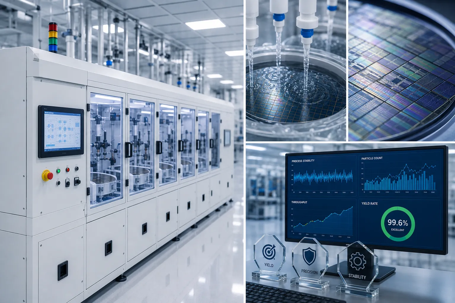
KOSEN SEMI Process Chamber: Closed-loop chemical recirculation and contamination defense.
Full-Stack Wet Process Equipment & System Ecosystem
A modular architecture integrating semiconductor wet bench systems, scrubber systems, and chemical process management for maximum wafer yield.
Semiconductor Wet Bench Platforms
Automated and semi-automated semiconductor wet bench systems engineered for ultra-pure etching, photoresist stripping, and surface conditioning.
Scrubber Systems & Cleaning
Advanced scrubber systems and megasonic wafer cleaning systems optimized for 200 nm standard defect reduction with capability down to 100 nm without pattern collapse.
Wet Bench Automation & Handling
Precision robotic transfer modules and micro-environment enclosures designed for reliable, vibration-free wafer transport in Single Wafer Cleaning Systems .
Chemical Process Management
High-purity chemical process management units offering inline concentration monitoring, auto-spiking, and eco-friendly waste recycling.
Semiconductor Equipment Integration
Turnkey software and hardware integration with full SECS/GEM compatibility, enabling real-time process control and smart fab automation.
Seamless Hardware & Software Synchronization
KOSEN SEMI delivers fully modular wet processing solutions optimized for yield maximization and rigorous cleanroom standards.
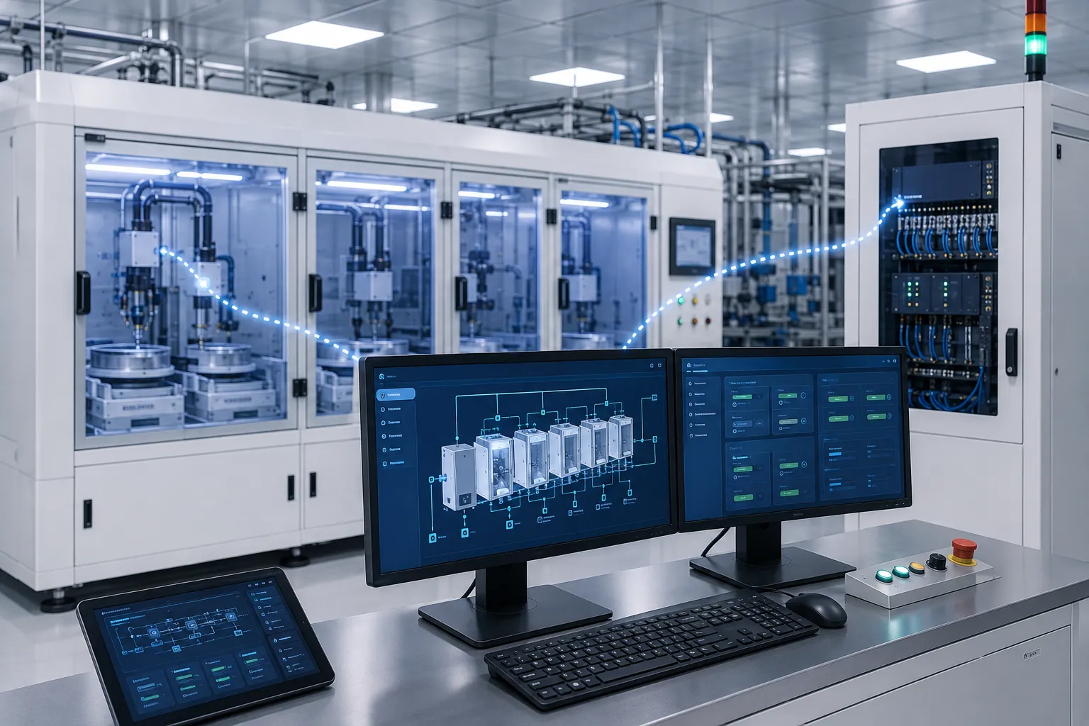
Industry 4.0 Process Control Systems & Wet Bench Automation
Closed-loop chemical dosing algorithms, low-vibration robotic handling, SECS/GEM smart fab connectivity, and ISO Class 5–7 cleanroom isolation.
Next-Generation Micro-Contamination Prevention Architecture
In advanced semiconductor fabrication, yield degradation is primarily driven by trace micro-particles, fluid cross-contamination, and chemical bath concentration drift. KOSEN SEMI integrates intelligent sensing architectures and real-time process control systems directly into every wet bench automation platform, supporting high-precision repeatability across continuous wafer fabrication runs.
Our automated chemical process management framework utilizes continuous inline spectrophotometry and micro-dosing metering pumps. The system dynamically compensates for bath degradation, chemical volatilization, and active constituent depletion. By maintaining chemical bath stability within micro-tolerances, semiconductor fabs prevent yield drop-offs during critical etching, stripping, and surface cleaning cycles. Backed by our advanced Engineering Capability, we ensure maximum process stability.
Engineering Insight: Closed-Loop Dosing Precision
Closed-loop chemical dosing continuously monitors fluid density, conductivity, and refractive index. It adjusts chemical injection rates within milliseconds to maintain exact chemical bath stoichiometry over hundreds of continuous operational hours.
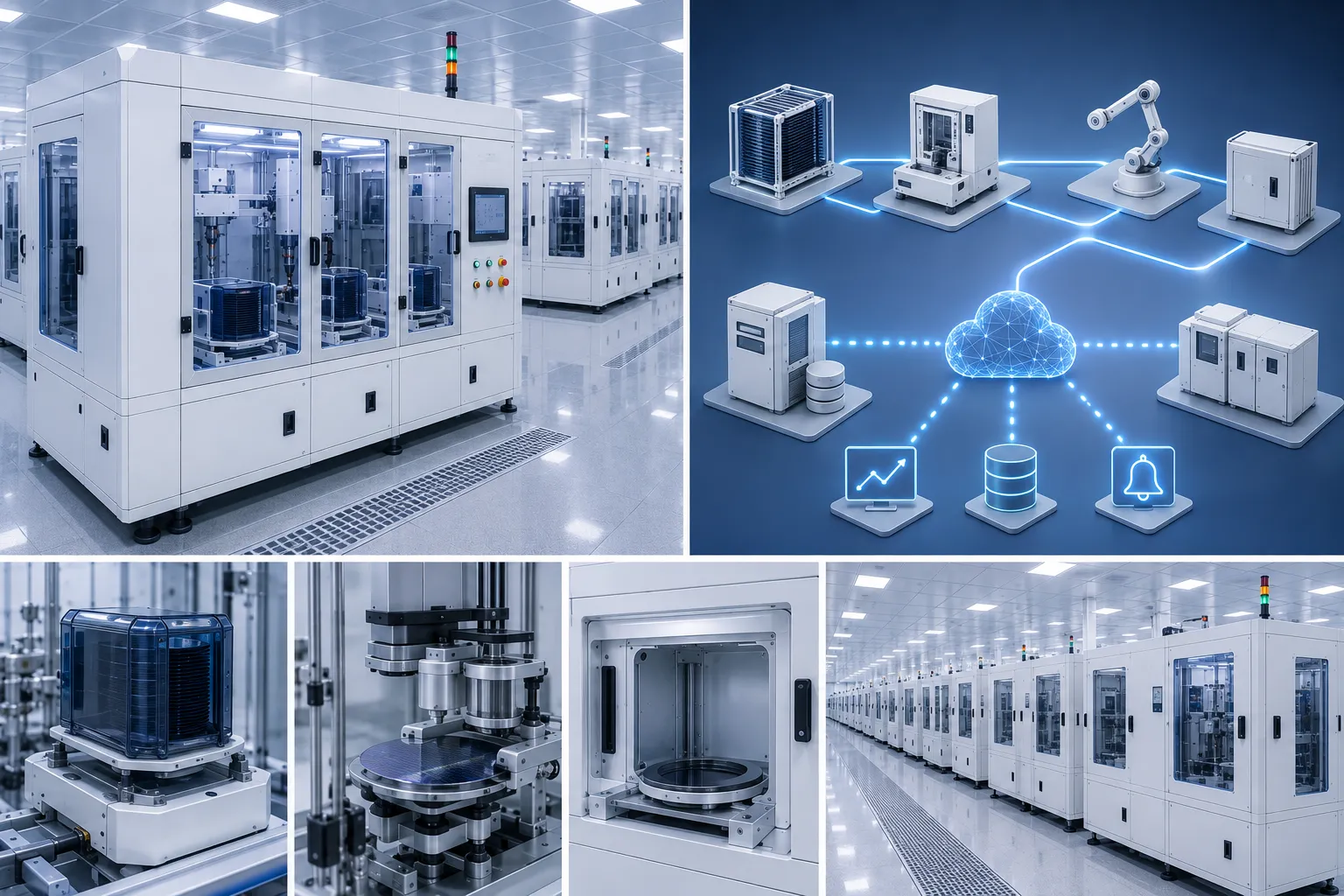
ISO Class 5–7 EFEM & SECS/GEM Smart Automation
Pillars of Automated Wet Bench Engineering
Comprehensive process control features engineered for high-throughput wafer yield enhancement. Discover how our Custom Wet Process Stations deliver uncompromised precision.
Vibration-Damped Edge-Handling Robotics
High-precision robotic end-effectors equipped with optical edge alignment achieve contact-free active area transfer. Custom acceleration profiles eliminate micro-vibrations and prevent fluid splashing during bath transfers.
- Low-scratch wafer edge contact mechanism
- Programmable multi-axis acceleration control
- Sub-millimeter spatial positioning accuracy
SECS/GEM Host Protocol Connectivity
Compliant with SEMI E30, E37, and GEM300 standards, our wet bench control systems connect directly to fab Manufacturing Execution Systems (MES) and Equipment Automation Programs (EAP) for automated recipe management.
- Real-time equipment telemetry & event logging
- Automated recipe validation and remote execution
- Fully compliant with lights-out fab architectures
ISO Class 5–7 Cleanroom Isolation Architecture
Integrated Equipment Front End Modules (EFEM) feature laminar HEPA/ULPA airflow filtration. Continuous positive interior pressure prevents ambient airborne particle ingress during high-speed wafer loading and unloading.
- ISO 14644-1, ISO Class 5–7 micro-environment
- Synchronized chemical vapor exhaust handling
- Active cross-contamination backflow prevention
Process Automation Performance Benchmarks
| Process Control Metric | Legacy Wet Processing Systems | KOSEN SEMI Smart Bench Platform | Wafer Yield Advantage |
|---|---|---|---|
| Particle Removal Sensitivity | 200 nm standard particle control | 100 nm optimized particle control efficiency | Eliminates defect drivers on fine-geometry wafers |
| Chemical Concentration Variance | ±0.5% (Manual titration / timed dosing) | ±0.1% (Inline closed-loop spectroscopy) | Supports consistent etch rates and surface cleanliness |
| Wafer Transfer Repeatability | ±0.25 mm (Mechanical centering) | ±0.02 mm (Optical vision guidance) | Prevents edge abrasion and structural micro-fractures |
| Fab Automation Integration | Standalone / Manual recipe selection | Full SECS/GEM GEM300 compliance | Enables fully autonomous, lights-out fab operations |
Download Process Control System Specifications
Explore comprehensive architectural schematics, SECS/GEM interface specification manuals, and real-world wafer yield verification reports.
Modular Semiconductor Equipment Integration & Turnkey Solutions
Customized engineering delivery from recipe validation and cleanroom manufacturing to seamless fab commissioning.
Turnkey Manufacturing Solutions Tailored to Modern Fabs
KOSEN SEMI provides advanced semiconductor equipment integration designed for high-volume manufacturing and legacy line retrofits. By unifying custom mechanical modeling, ultra-pure fluidics, and automated SECS/GEM interface controls, our turnkey manufacturing solutions accelerate production ramp-up while reducing total cost of ownership.
Target Tool Uptime Reliability
Cleanroom Manufacturing Standard
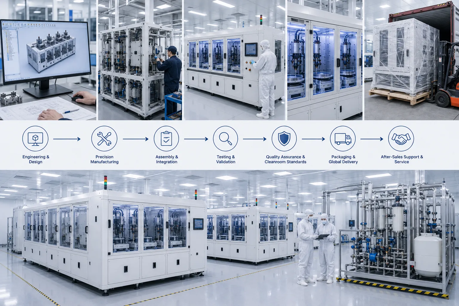
Our 5-Step Engineering Delivery Process
End-to-end integration architecture backed by our advanced Engineering Capability, engineered for consistent quality execution, rapid qualification, and long-term yield stability.
Recipe & Process Diagnostics
Comprehensive evaluation of target process chemistries, wafer specs, and facility utilities to establish precise engineering parameters.
Custom Modular Engineering
3D mechanical and fluidic modeling engineered to optimize tool footprint, prevent chemical contamination, and ensure seamless hardware fit.
Cleanroom Assembly & Build
Precision component manufacturing and sub-assembly inside certified ISO Class 5–7 cleanrooms with helium leak integrity testing.
FAT / SAT & Commissioning
Rigorous Factory and Site Acceptance Testing (FAT/SAT), facility hookup verification, and automated MES software integration.
Continuous Lifecycle Support
24/7 field engineering response, preventative maintenance schedules, and modular upgrades for evolving fab processes.
Submit Your Custom Integration Requirements
Partner with KOSEN SEMI to develop high-yield, modular semiconductor equipment integration tailored to your fab line specifications.
Semiconductor Wet Process Technical FAQ & Selection Guide
In-depth technical answers regarding substrate compatibility, fluoropolymer chemical resistance, damage-free megasonic energy, and legacy fab retrofits.
Which wafer substrate materials and diameters does KOSEN SEMI equipment support?
KOSEN SEMI semiconductor wet process technology platforms natively support standard 150mm, 200mm, and 300mm wafer diameters across both single-wafer wet cleaning tools and automated batch Automatic Wet Bench Systems configurations.
Our processing chambers, fluid dispensing arms, and chemical management systems adapt seamlessly to diverse substrate chemistries and physical specifications:
- Monocrystalline Silicon: Prime, ultra-thin, and reclaimed silicon wafers for 200 nm standard and 100 nm optimized logic processes, DRAM, and 3D NAND applications.
- Compound Semiconductors: Silicon Carbide (SiC) and Gallium Nitride (GaN) power device substrates with specialized thermal control and etching recipes.
- Advanced & Optoelectronic Substrates: Gallium Arsenide (GaAs), Indium Phosphide (InP), Glass, and Quartz for RF, photonics, and advanced packaging applications.
Every tool incorporates programmable Bernoulli chuck dynamics and non-contact edge-grip robotic end-effectors to prevent micro-fractures, edge chipping, and backside wafer surface contamination during ultra-pure chemical processing.
How does KOSEN SEMI support chemical resistance and hardware longevity against aggressive chemistries?
To withstand aggressive wafer processing technology chemistries—including hydrofluoric acid (HF), sulfuric peroxide mixture (SPM), SC1, SC2, and solvent strip formulations—KOSEN SEMI constructs all direct fluid contact pathways using ultra-pure fluoropolymers.
- 100% Fluoropolymer Wetted Paths: High-purity PFA, PTFE, and PVDF components eliminate metallic ionic contamination, leachables, and particulate degradation.
- Infrared Fusion Welding: Seamless pipe joining eliminates mechanical fittings, dead zones, and microscopic particulate entrapment crevices.
- Secondary Containment Enclosures: Dual-containment chemical reservoirs and real-time leak detection fulfill stringent SEMI S2 and SEMI S8 safety standards.
This robust material architecture supports high chemical purity, low leachable levels, extended component operational life, and high tool availability during continuous fabrication.
How does megasonic cleaning achieve 200 nm standard particle removal with optimized capability down to 100 nm without damaging delicate wafer structures?
Conventional low-frequency acoustic cleaning produces uncontrolled cavitation that damages fragile, high-aspect-ratio fine features within the 200 nm standard and 100 nm optimized capability range. KOSEN SEMI megasonic wafer cleaning systems utilize high-frequency acoustic field sweeping to achieve gentle, uniform micro-particle displacement.
Megasonic Safety & Efficiency Innovations
- Frequency Sweeping (0.8 MHz – 3.0 MHz): Eliminates acoustic standing waves and hot spots, ensuring uniform power distribution across the whole wafer surface.
- Boundary Layer Acoustic Streaming: Generates micro-scale fluid motion to overcome particle adhesion forces at 200 nm under standard conditions and down to 100 nm under optimized conditions without causing structural pattern collapse.
- Closed-Loop Transducer Feedback: Real-time digital power monitoring prevents energy spikes and preserves sensitive FinFET and gate structures.
This precise energy transfer achieves superior particle removal performance validated for each process recipe while preserving 3D NAND and advanced logic pattern integrity.
Can KOSEN SEMI wet processing modules retrofit existing legacy fab production lines?
Yes. KOSEN SEMI semiconductor wet bench and cleaning modules feature modular physical and software architectures engineered specifically for legacy fab retrofits and floor-space constrained cleanrooms.
- Flexible Chassis Footprint: Custom physical layouts align directly with tight cleanroom footprints, existing utility drop points, and exhaust routing.
- SECS/GEM Fab Automation Compliance: Standardized software protocols connect directly with legacy Manufacturing Execution Systems (MES) for total lot tracking.
- Modular Subsystem Integration: Chemical supply units, scrubber systems, and IPA Marangoni dryer modules can be retrofitted onto third-party wet benches.
Our application and field service engineering teams perform complete mechanical mounting, utility hookups, software protocol handshakes, and recipe validation with minimal impact on active fab schedules.
How does chemical dosing precision impact wafer yield enhancement in critical wet processes?
Accurate ratio management is vital for consistent etch rates, residue removal, surface passivation, and chemical bath longevity. Uncontrolled chemical mixing causes concentration drift, leading to non-uniform etching and yield loss.
KOSEN SEMI integrates real-time closed-loop chemical process management systems to maintain continuous process window stability:
- Inline Real-Time Analytics: Near-infrared optical refractometers and conductivity sensors continuously track chemical concentration ratios.
- High-Precision Dosing Systems: Micro-metering injection pumps maintain chemical mixture tolerances within an ultra-tight ±0.1% window.
- Automated Chemical Spiking: Dynamic replenishment algorithms inject precise reagent volumes to stabilize bath performance during high-throughput runs.
By stabilizing chemical kinetics and extending bath longevity, fabs achieve predictable process windows, lower chemical consumption, and measurable wafer yield enhancement.
What drying technologies are deployed to eliminate watermarks on complex wafer topography?
Watermarks form when residual deionized water droplets evaporate on silicon surfaces, leaving silica residues and localized oxide defects. KOSEN SEMI employs advanced IPA Marangoni dryer systems combined with surface tension gradient control to deliver low-defect drying.
During controlled wafer withdrawal from ultraclean DI water, vaporized Isopropyl Alcohol (IPA) creates a surface tension differential at the liquid meniscus. This Marangoni force pulls liquid cleanly off hydrophobic and hydrophilic surfaces simultaneously, supporting low watermark residue levels even in deep contact vias and dense micro-trenches.
Process Selection Matrix
Quick reference matching wafer processing technology modules with semiconductor manufacturing applications.
| Application | Tool Architecture | Core Tech |
|---|---|---|
| FEOL Wafer Cleaning | Single Wafer System | Megasonic Sweeping |
| Bulk Photoresist Strip | Batch Wet Bench | Recirculating SPM |
| Compound Semiconductors | Scrubber Systems | High-Pressure Spray |
| Watermark Elimination | Dryer Module | IPA Marangoni |
Need Custom Wet Process Parameters?
KOSEN SEMI application engineers provide chemical evaluations, fluid dynamic simulations, and cleanroom hardware selection for unique fab throughput targets.
- Substrate chemical compatibility testing
- SECS/GEM protocol custom alignment
- ISO Class 5–7 cleanroom isolation compliance
Quality Assurance & Fab Standard Compliance
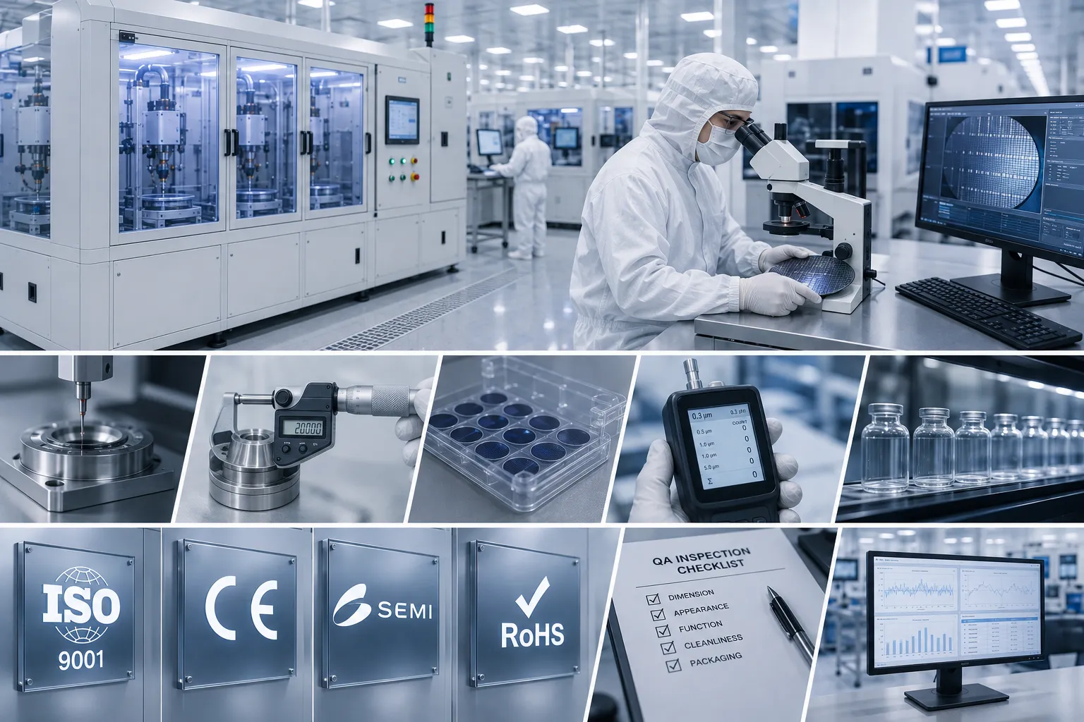
Every KOSEN SEMI semiconductor wet process system undergoes rigorous factory acceptance testing (FAT) prior to site installation. Our semiconductor equipment integration platforms satisfy SEMI S2, SEMI S8, and ISO 14644-1, ISO Class 5–7 cleanroom particle emission standards to accelerate immediate fab qualification.
Ready to Elevate Your Wafer Cleaning Systems Yield and Line Throughput?
Connect directly with KOSEN SEMI process specialists to configure high-precision, custom wet process solutions tailored to your fab.
Discuss your process, equipment, and integration requirements with KOSEN SEMI.