
Semiconductor Wet Process Technology & Precision Equipment Platforms
Maximize wafer yield with KOSEN SEMI wet process technology. Engineered for ultra-clean wafer-cleaning-systems, high-selectivity wet etching, resist stripping, and precise surface preparation across front-end and back-end semiconductor manufacturing. Learn more about our team on our about-us page.
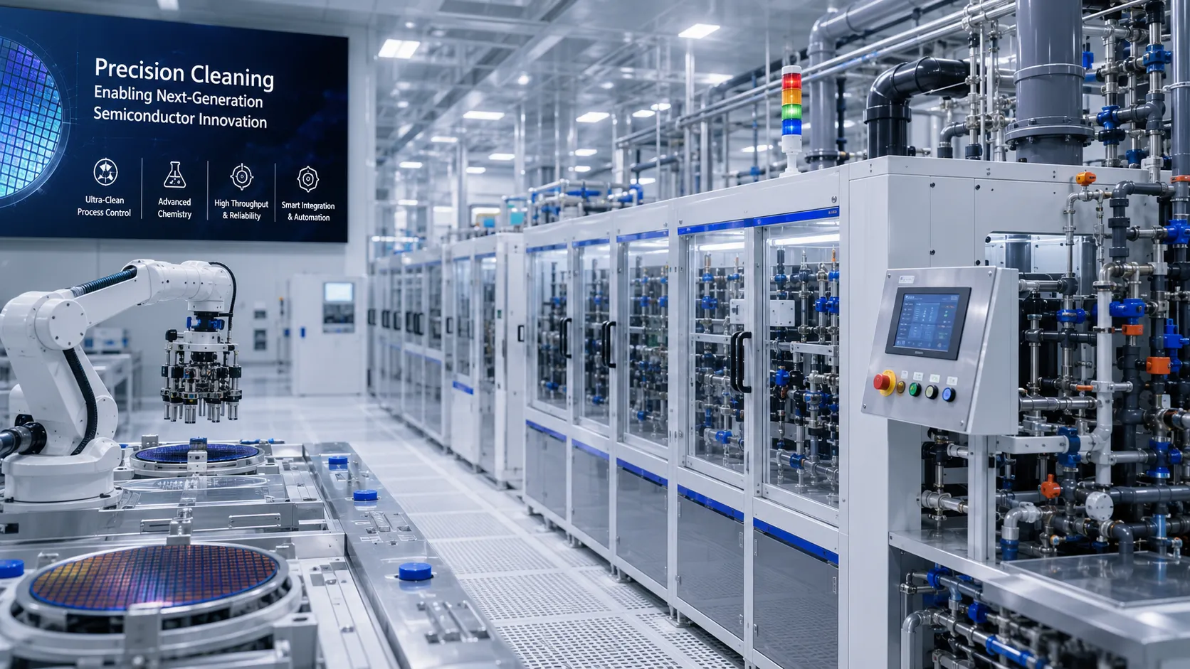
Wet Process Equipment Architecture & Physical-Chemical Control Systems
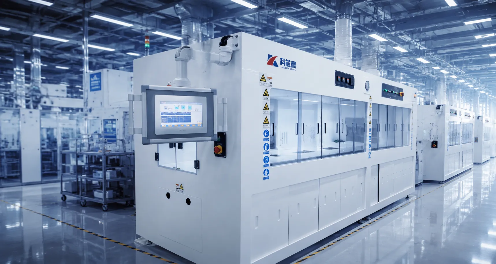
KOSEN SEMI engineers high-reliability wet process equipment architecture built around three foundational engineering pillars, reflecting our advanced Engineering Capability. By synchronizing closed-loop chemical delivery systems, multi-frequency megasonic wave cavitation, and automated substrate handling within isolated environments, our wafer-cleaning-systems deliver exceptional semiconductor manufacturing precision and physical-chemical bath stability across both front-end and back-end fabrication nodes, including dedicated Single Wafer Cleaning Systems.
High-Precision Fluid & Chemical Delivery Systems
Our automated chemical delivery system maintains precise bath composition, real-time chemical concentration, and dynamic fluid dynamics under high-throughput production to prevent bath degradation and extend operational life.
- Closed-Loop Dosing: In-line spectroscopic concentration sensors trigger automated micro-dosing pumps to maintain exact molar ratios during continuous operation.
- Micro-Flow Regulation: Ultra-fast mass flow controllers and pulse-suppressed pumps regulate fluid velocity without introducing supply-line pressure spikes.
- Thermal Stabilization: Direct PTFE chemical heaters and heat exchangers maintain bath temperatures within strict operational thresholds.
Multi-Frequency Megasonic & Ultrasonic Cleaning
Advanced acoustic wave generators distribute controlled sound fields throughout chemical baths to detach particles without damaging delicate fine-scale features or pattern geometries.
- Cavitation Control: Uniform acoustic pressure removes particulate contamination down to 100 nm under optimized conditions while guarding against structural pattern damage.
- Multi-Frequency Switching: Broad operating range from 800 kHz to 3 MHz allows targeted acoustic energy tuning per process step.
- Acoustic Uniformity: Engineered transducer arrays minimize acoustic dead zones and local energy hotspots across 200mm and 300mm wafers.
Modular Automated Handler & Isolation Chamber
High-speed robotic transfer arms integrate with sealed micro-environment chambers to protect substrates against cross-bath vapor transport and airborne contamination.
- Robotic Precision: High-purity PEEK end-effectors driven by servo mechanics deliver sub-millimeter wafer transfer positioning accuracy.
- Laminar Flow Control: ISO Class 5–7 mini-environments featuring ULPA filtration maintain clean, uniform downward air velocities.
- Anti-Cross Contamination: Automated chamber covers and dynamic drip management isolate chemical vapors between individual process stations.
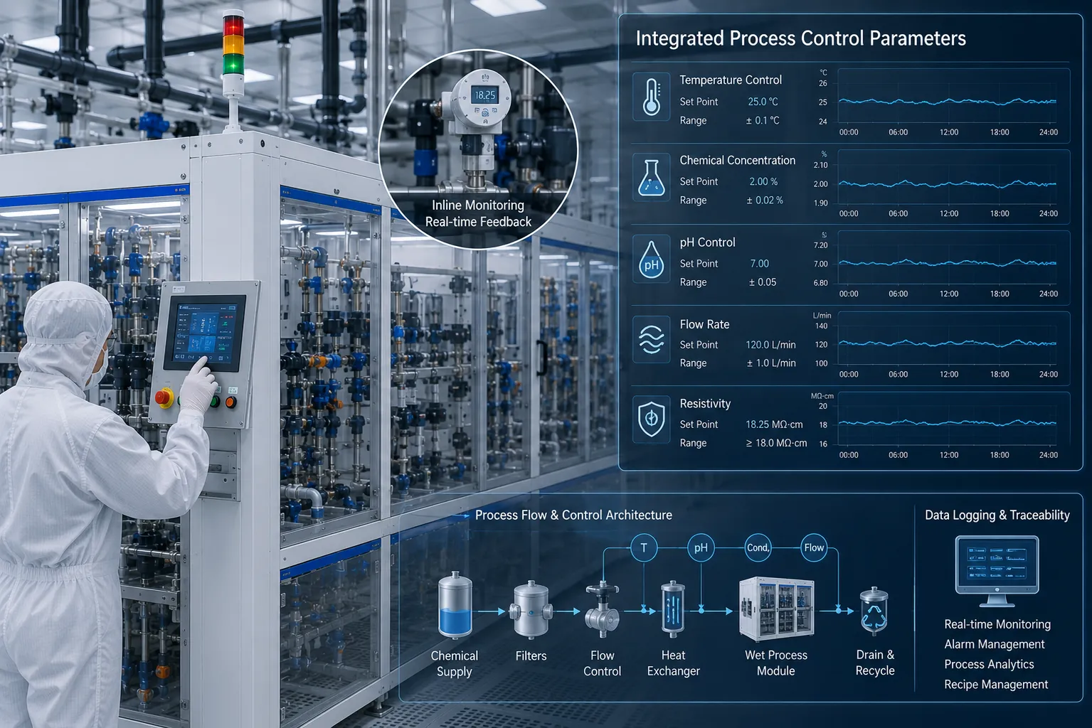
Integrated Process Control Parameters
KOSEN SEMI equipment architecture pairs hardware limits with automated inline physical-chemical management to support consistent process margins and fab yield optimization.
| Sub-Assembly System | Primary Control Parameter | Standard Limit |
|---|---|---|
| Chemical Delivery System | Inline Concentration Accuracy | ±0.05% |
| Thermal Control Module | Recirculating Bath Thermal Stability | ±0.1°C |
| Megasonic Transducer Array | Particle Removal Efficiency (≥200 nm) | Application Dependent |
| Automated Robotic Handler | Wafer Transfer Repeatability | ±0.02 mm |
Critical Process Nodes: Wafer Cleaning, Etching, Stripping & Drying
KOSEN SEMI delivers application-driven wet process technology engineered for high-yield front-end-of-line (FEOL) and back-end-of-line (BEOL) semiconductor manufacturing. From advanced 300mm logic and memory foundries to mature 200mm power discrete and compound semiconductor (SiC/GaN) lines, our equipment platforms deliver uncompromising particle control, tight chemical uniformity, and absolute substrate safety across every critical process node. Explore our full range of semiconductor products to learn more.
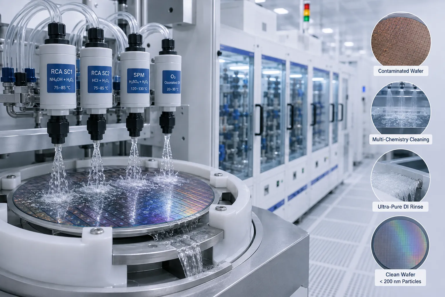
Ultra-Clean Wafer Cleaning
As semiconductor device features shrink, controlling fine particulate contaminants becomes vital to achieving target wafer yields. KOSEN SEMI wafer-cleaning-systems leverage optimized RCA (SC1/SC2), SPM (sulfuric peroxide mixture), and ozonated chemistry sequences to strip organic residues, metallic ion contaminants, and 200 nm-class particulate contamination while minimizing substrate surface degradation risk.
- 200 nm-Class Particle Removal: High-efficiency megasonic-assisted agitation dislodges micro-particulates down to 100 nm under optimized conditions without damaging delicate fine structures.
- Chemical Delivery Control: Closed-loop chemical dosing and inline recirculation maintain exact SPM, HF, and RCA bath stoichiometric ratios.
- Cross-Contamination Barrier: Isolated dual-containment process chambers ensure metallic ion threshold levels stay below 1E10 atoms/cm².
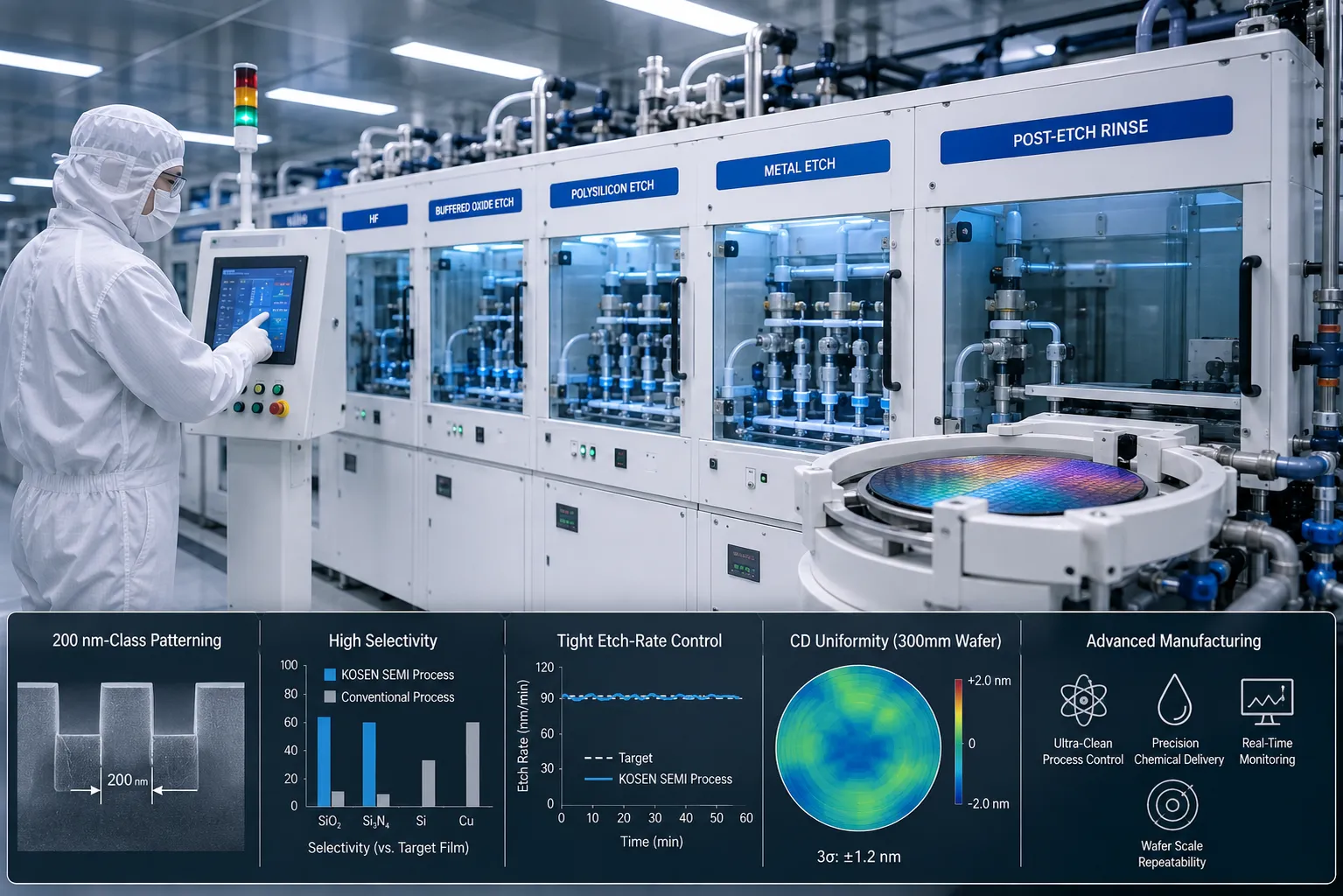
High-Selectivity Wet Etching
200 nm-class thin-film patterning requires exceptional chemical selectivity to protect underlying dielectric, silicon, and metal layers during processing. KOSEN SEMI high-selectivity wet etching platforms deliver precise isotropic and anisotropic film removal with tight etch-rate control and repeatable critical dimension (CD) performance across 200mm and 300mm wafer substrates by using Engineering Capability designed for advanced manufacturing.
- Etch Rate Uniformity: Dynamic bath fluidics achieve tight within-wafer and wafer-to-wafer etch rate uniformity within ±1.5%.
- Sub-degree Thermal Tuning: Real-time closed-loop chemical bath heating and cooling hold process temperatures strictly within ±0.1°C.
- Substrate Versatility: Optimized chemistry management for silicon oxide, silicon nitride, aluminum, copper, and SiC/GaN substrates.
Photoresist Stripping
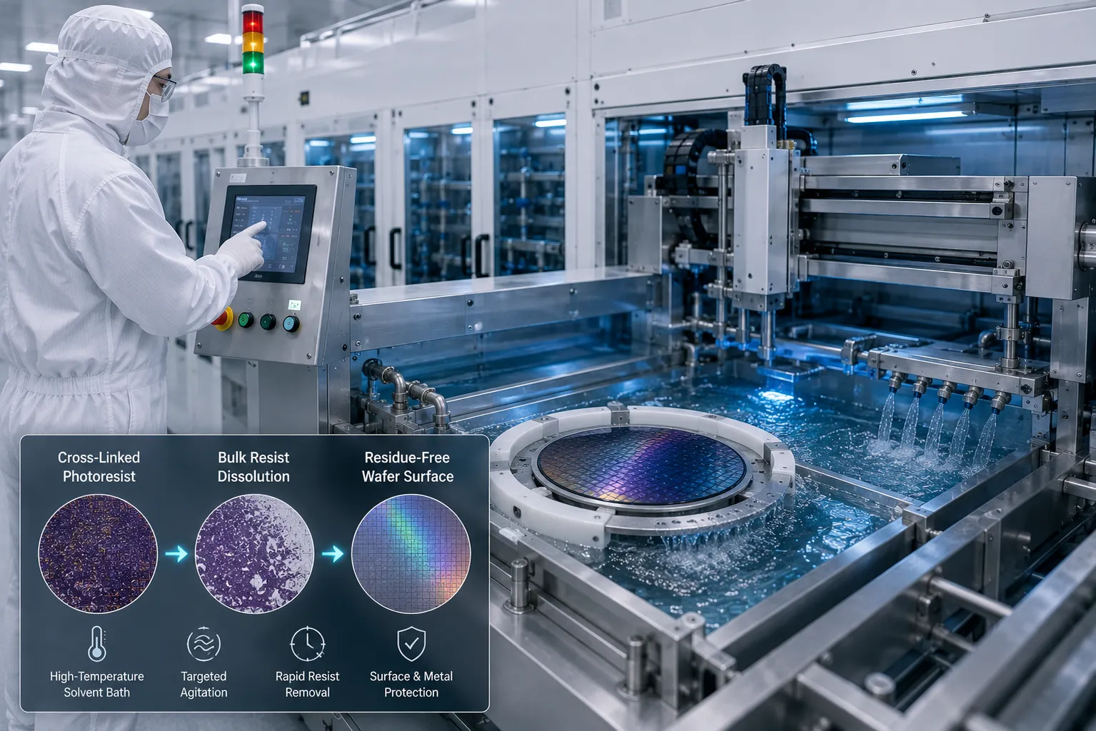
High-dose ion implantation and aggressive plasma etch steps leave heavily cross-linked photoresist crusts and resilient ash residues. KOSEN SEMI photoresist stripping modules integrate high-temperature solvent bath processing with targeted agitation to perform rapid bulk resist dissolution and complete post-etch residue removal without substrate surface oxidation or interconnect metal corrosion.
- Substrate Preservation: Formulated chemistries minimize active-silicon oxidation and galvanic-corrosion risks on metallic interconnects.
- Hardened Polymer Breakdown: Targeted solvent spray arrays penetrate heavily cross-linked polymers and post-implant residues effortlessly.
- Solvent Reclamation Integration: Automated chemical segregation and solvent recycling dramatically decrease CoO and environmental overhead.
Surface Preparation & Advanced Drying
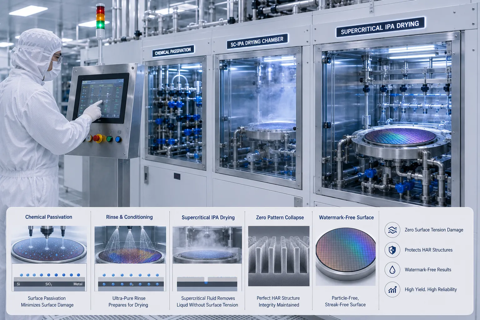
In semiconductor manufacturing, surface tension forces during traditional spin drying can cause pattern collapse across high-aspect-ratio (HAR) structures. KOSEN SEMI surface preparation technology pairs controlled chemical passivation with supercritical isopropyl alcohol (IPA) drying to reduce pattern-collapse and watermark risks.
- Reduced Pattern-Collapse Risk: Supercritical IPA drying reduces capillary surface-tension forces on delicate high-aspect-ratio trenches.
- Watermark-Free Surface: In-situ chemical passivation inhibits native oxide growth and prevents drying-induced watermark defects.
- Tailored Surface Energy: Precise hydrophobic and hydrophilic surface termination optimizes downstream ALD, CVD, and epitaxy growth.
Wet Process vs. Dry Process: Complementary Capabilities in Semiconductor Fabs
Evaluate critical performance metrics across wet chemical processing vs dry plasma processing. Discover how KOSEN SEMI wet benches deliver superior particle removal efficiency, chemical selectivity, and cost of ownership in high precision semiconductor processing. Backed by our advanced Engineering Capability, our solutions support semiconductor manufacturers and fab users worldwide.
| Evaluation Parameter | Wet Chemical Processing (KOSEN SEMI) | Dry Plasma Processing | Process Advantage |
|---|---|---|---|
| Particle Removal Efficiency | High removal performance for 200 nm-class contaminants using megasonic chemistry baths, subject to process conditions. | Limited physical particle removal capability. High risk of chamber wall byproduct redeposition. | Wet Process |
| Substrate Damage & Radiation | Low physical or plasma-induced damage (PID) risk to delicate surface microstructures and gate oxides. | Elevated risk of crystal lattice damage and surface charge accumulation from high-energy ion bombardment. | Wet Process |
| Thermal Budget Impact | Low-temperature chemical bath operations preserve tight thermal budgets across sensitive process steps. | Elevated wafer temperatures and localized thermal stress caused by high-power plasma exposure. | Wet Process |
Maximizing Fab Yield Through Hybrid Wet/Dry Workflows
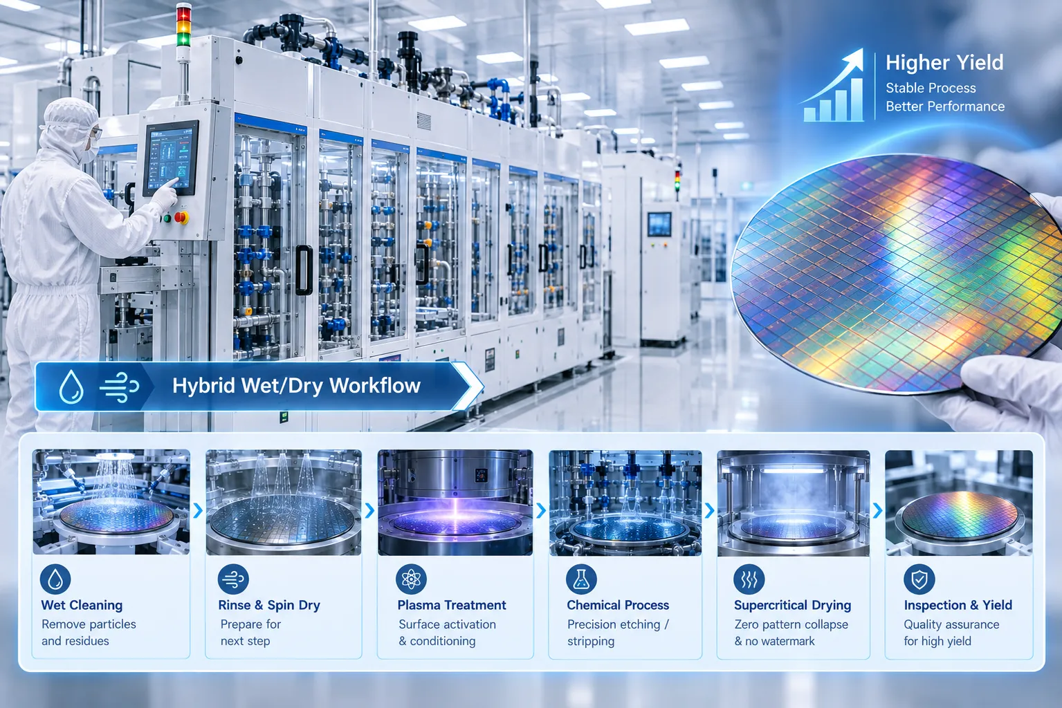
Analyzing wet process vs dry process trade-offs is essential for advanced yield optimization. Modern semiconductor fabs achieve maximum productivity by integrating KOSEN SEMI automated wet benches alongside dry plasma etching and CVD cluster tools, as well as dedicated Single Wafer Cleaning Systems.
High precision semiconductor processing ensures atomically clean surfaces free of native oxides prior to CVD dielectric growth.
Targeted wet chemistry strips plasma etch residues and fluorocarbon polymers efficiently without damaging underlying films.
Hardware Specifications & Quantifiable Process Control Limits
Engineered to pass technical audits by senior process engineers, yield experts, and fab directors, KOSEN SEMI wet processing equipment establishes verifiable baselines for modern semiconductor manufacturing. Our platforms maintain operational parameter boundaries across fluid dynamics, chemical bath stability, and 200 nm-class wafer cleaning systems performance.
Precision Engineering Control Limits
200 nm-class process windows require physical and chemical hardware controls that reduce batch-to-batch variation. KOSEN SEMI integrates automated multi-variable feedback loops, high-purity fluoropolymer fluid handling, and advanced sensors backed by our extensive Engineering Capability to support uniform chemical exposure.
Particle Level Control
200 nm-class defect mitigation
Maintains particle level control with fewer than 5 particle adders at sizes at or above 200 nm per wafer pass. PFA point-of-use micro-filtration combined with controlled megasonic energy delivery strips fine particulate contaminants while minimizing risk to delicate circuit topographies.
Chemical Temperature Control
Thermal uniformity & reaction kinetics
Provides ±0.1°C real-time closed-loop chemical temperature control across recirculation baths. Multi-channel PID controllers and inline heat exchangers counteract thermal drops during chemical replenishment, protecting etch rates and chemical concentrations.
Cross-Contamination Boundary
Trace metallic purity management
Designed to maintain surface metallic contamination below 1E10 atoms/cm² under validated process conditions. Sealed processing chambers, dedicated exhaust partitioning, and laminar air movement reduce cross-bath vapor drag and airborne trace metal migration.
Throughput Efficiency
High-UPH automated handling
Maximizes overall throughput efficiency through automated dual-stage robotic end-effectors, integrated seamlessly into our Single Wafer Cleaning Systems. Dynamic scheduling algorithms balance chemical dwell times with rapid transfer motion to deliver continuous fab utilization.
Process Control Specification Matrix
Fab Benchmark Comparison| Engineering Parameter | Legacy Tool Baseline | KOSEN SEMI Verified Standard |
|---|---|---|
| Particle Adder (≥200 nm) | < 15 particles/wafer | < 5 particles per wafer pass |
| Chemical Temp Control | ±0.5°C to ±1.0°C | ±0.1°C closed-loop tuning |
| Metallic Impurities | < 1E11 atoms/cm² | < 1E10 atoms/cm² threshold |
| Wafer Drying Residue | < 2 marks per wafer | Low watermark risk (Supercritical IPA) |
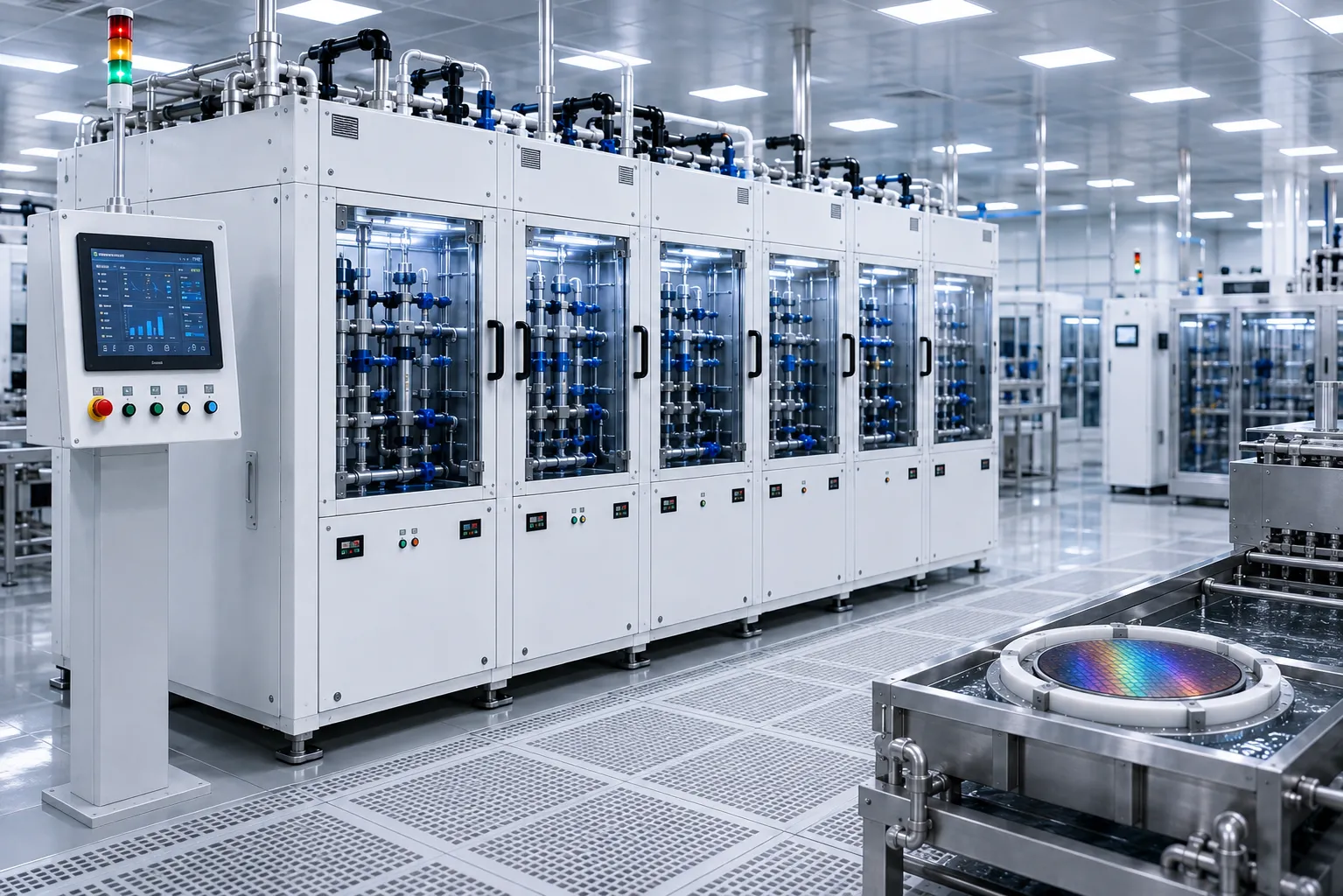
Live Process Audit Display
Factory Acceptance Testing (FAT) Standard
KOSEN SEMI equipment undergoes rigorous Factory Acceptance Testing before delivery. Platforms complete 100-hour continuous stability runs, multi-point chemical temperature control verification, and trace metal analytical testing to support cleanroom integration.
Cleanroom & Safety Compliance
Fully compliant with SEMI S2/S8 standards and ISO 14644-1 Class 5–7 cleanroom environments, simplifying Site Acceptance Testing (SAT) for semiconductor fabs globally.
Global Semiconductor Safety Standards & Cleanroom Compliance
KOSEN SEMI builds all wet process platforms in strict alignment with international semiconductor safety standards. By integrating certified environmental, structural, and operational safeguards into our Automatic Wet Bench Systems and custom designs, we streamline customer fab acceptance audits and simplify global fab expansions.
SEMI S2 & SEMI S8
Engineered for full SEMI S2 compliance and ergonomic excellence, offering advanced hazard containment, electrical safety, and complete operator protection.
ISO 14644-1 Class 5–7
Supports cleanroom compatibility for ISO Class 5–7 fab environments with optimized exhaust control to minimize airborne particulate risks.
CE & FM 4910 Compliance
Combines European CE mark compliance with FM 4910 fire-retardant plastic cabinet materials to ensure long-term structural integrity and fire safety.
ISO 9001 & Chemical Safety
Features complete ISO 9001 component traceability supported by our advanced Engineering Capability along with explosion-proof chemical cabinet design, leak detection, and automated shutoff protection.
Accelerate On-Site Fab Acceptance Audits (SAT)
Pre-verified wet processing equipment architectures remove compliance roadblocks during commissioning. KOSEN SEMI delivers fully documented systems tailored to clear third-party fab audits effortlessly.
Semiconductor Wet Process Technology & Selection FAQ
Navigating semiconductor wet process equipment selection requires precise alignment between chemical mechanics, hardware architecture, and yield targets. Explore authoritative technical insights from KOSEN SEMI application engineers regarding compound semiconductor customization, chemical bath longevity, production lead times, and environmental compliance in this wet process technology FAQ guide.
Does KOSEN SEMI support custom wet bench configurations for compound semiconductors like SiC or GaN?
Yes. KOSEN SEMI specializes in custom semiconductor equipment selection, engineering tailored single-wafer and automated batch wet processing platforms specifically for high-hardness, chemically inert compound semiconductor substrates including Silicon Carbide (SiC), Gallium Nitride (GaN), and Gallium Arsenide (GaAs).
Our specialized SiC wet bench design incorporates high-efficiency acoustic transducers for multi-frequency megasonic wafer cleaning systems, elevated-temperature acid recirculation baths for aggressive chemistries (such as hot H3PO4 and SPM), and precision micro-fluidic chemical delivery. These dedicated process modules prevent micro-fracturing and thermal stress while ensuring complete surface residue removal and particle level control down to 100 nm under optimized conditions across 150mm and 200mm compound wafer manufacturing lines.
How is chemical tank longevity supported when handling aggressive chemistries like HF or SPM?
Chemical bath structural integrity is vital to maintaining operational safety and preventing costly fab downtime. KOSEN SEMI process baths are constructed exclusively from ultra-high purity, stress-relieved polymers and quartz tailored to specific chemical dynamics:
- Hydrofluoric Acid (HF) Baths: Fabricated using premium PVDF and PTFE with stress-relieved thermal welding techniques that reduce joint fatigue, chemical embrittlement, and micro-cracking risks during extended etch cycles.
- Sulfuric Peroxide Mixture (SPM) Baths: Constructed with high-purity fused quartz and PFA liners designed to withstand continuous thermal shocks up to 150°C and exothermic chemical reactions during heavy organic photoresist stripping.
Every bath assembly undergoes rigorous thermal cycling stress tests and non-destructive weld inspections to minimize trace-leaching risk, support chemical compatibility, and promote long operating life in production cleanrooms.
What is the typical lead time from requirement evaluation to Site Acceptance Testing (SAT)?
Equipment delivery timelines are strictly managed through KOSEN SEMI's structured engineering and manufacturing protocol to support rapid fab expansion and line qualification:
Our end-to-end milestone protocol covers initial process modeling, 3D fluid dynamics simulation, Factory Acceptance Testing (FAT) at KOSEN SEMI facilities, cleanroom installation, and final Site Acceptance Testing (SAT) on production wafer lots.
How does the equipment handle chemical waste segregation and environmental recycling?
KOSEN SEMI wet processing tools incorporate automated multi-route chemical waste drain manifold systems managed by flexible recipe logic to maximize environmental sustainability and fab compliance:
- Automatic Stream Segregation: Dedicated point-of-use drain valves route chemical waste into isolated recovery lines for concentrated acids, alkali solutions, organic solvents, and toxic effluents without cross-contamination.
- IPA & Solvent Recovery: Integrated supercritical Isopropyl Alcohol (IPA) drying modules capture and route vapor condensate back into closed-loop purification loops, reducing solvent usage by up to 40%.
- Effluent Neutralization Interfacing: Inline chemical conductivity and pH monitoring sensors continuously verify drain streams to ensure seamless compliance with facility wastewater treatment standards.
How do engineers determine whether single-wafer or batch processing is appropriate?
Selecting the optimal wet process architecture depends on process node parameters, wafer diameter, defectivity limits, and target throughput (UPH):
Single-Wafer Processing: Recommended for 200 nm standard processes, with optimized capability down to 100 nm, high-aspect-ratio feature cleaning, and defect-sensitive steps where minimized cross-contamination, boundary-layer control, and precise Single Wafer Cleaning Systems spin-spray delivery are required.
Batch Wet Benches: Ideal for high-throughput front-end-of-line (FEOL) bulk wafer cleaning, resist stripping, and wet etching applications where maximizing UPH and minimizing Cost of Ownership (CoO) drive production efficiency.
Custom Technical Consultation
Facing specialized chemical delivery needs, non-standard substrate geometry, or strict particle adder constraints on your semiconductor line?
Collaborate directly with KOSEN SEMI application specialists to formulate custom equipment specifications and process recipes.
Full international cleanroom safety, environmental compliance, and ergonomic certification across all wet bench systems.
Need Custom Wet Bench Specs?
Download detailed hardware schematics, fluid dynamics blueprints, and cleanroom integration specifications for your fab.
Request a Custom Semiconductor Wet Process Solution
Ready to Elevate Wafer Yield and Accelerate Wet Process Throughput?
Contact semiconductor engineers at KOSEN SEMI to review chemical compatibility, configure tailored equipment architectures, or request a wet bench quote for your fab. Learn more about our Engineering Capability in providing custom solutions.
Direct Access to Senior Application Specialists
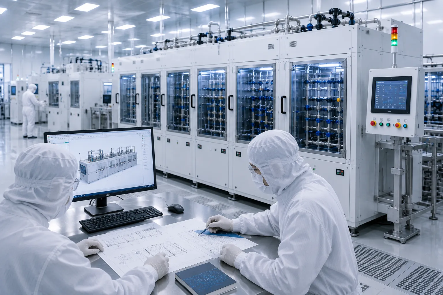
Collaborate directly with our technical team to evaluate single-wafer processing, automated batch wet bench design, and chemical delivery system integration tailored to your fab requirements.
Custom
Fab-Tailored
<24 Hours
Engineer Response