
Custom Semiconductor Equipment Engineered to Your Exact Process Requirements
Break through standard tool limitations. As a leading semiconductor equipment manufacturer, KOSEN SEMI leverages advanced Engineering Capability to provide turnkey engineering solutions and tailored wet processing tools to meet your precise fab requirements.
100% Process Matching
Custom engineered to match your specific chemical recipes, substrate sizes, and yield goals.
Flexible Modular Design
Scalable architecture designed for seamless fab integration, cleanroom footprint optimization, and upgrades.
SEMI Safety Compliant
Strict alignment with global SEMI S2/S8 safety and environmental standards for risk-free operation.
Full Engineering Delivery
Complete project lifecycle support from initial CFD simulation to FAT/SAT validation and commissioning.
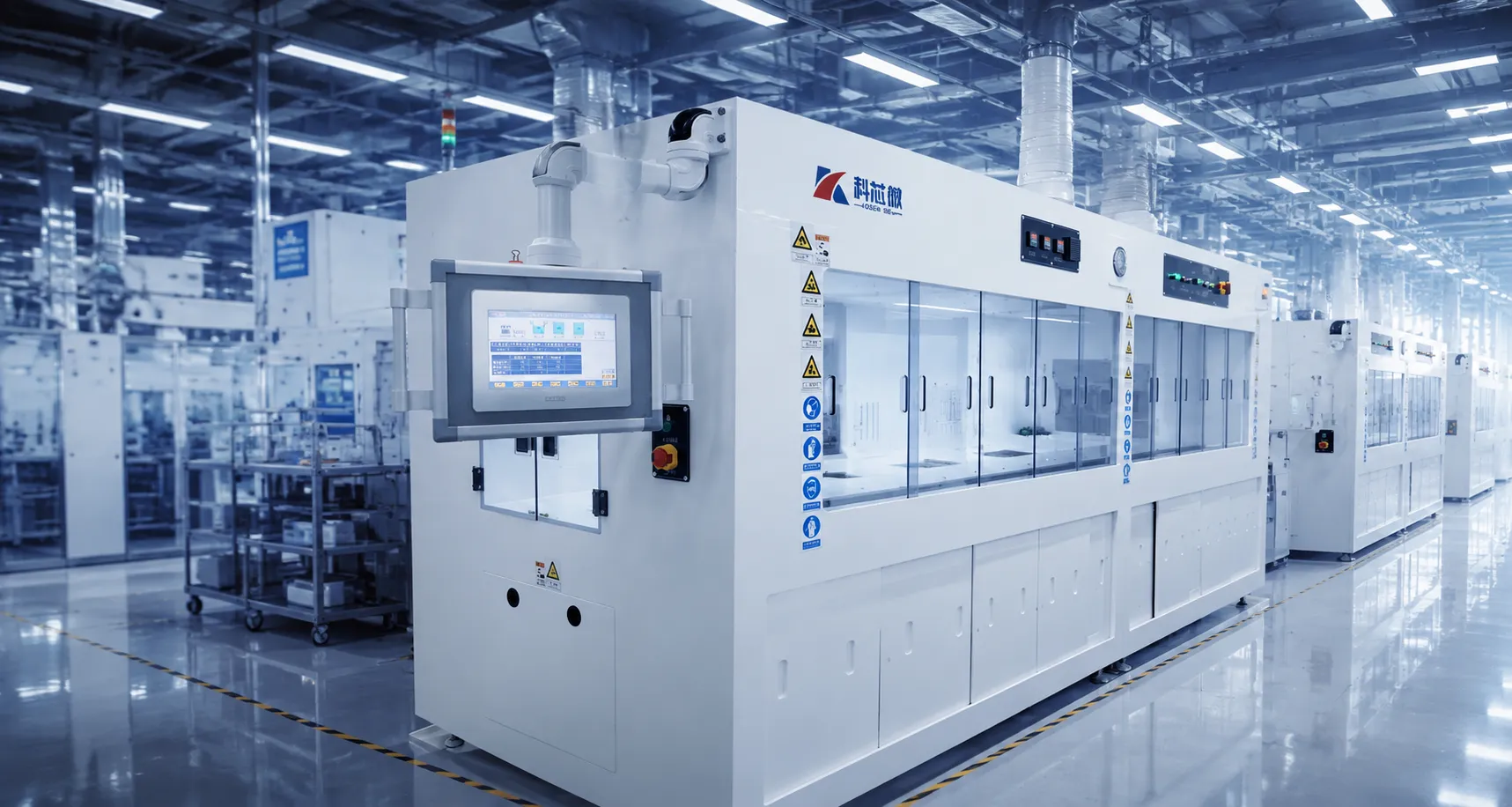
Custom Wet Process Platform
High-Precision Tooling Architecture
Custom Engineering Capabilities & Modular Technology Matrix
KOSEN SEMI provides application-driven custom semiconductor equipment engineered to overcome the constraints of standard processing tools. Backed by dozens of patented innovations, our engineering team delivers tailored wet processing solutions, specialized cleaning architectures, and integrated environmental scrubbers optimized for complex substrate chemistries, non-standard wafer sizes, and demanding fab environments.
Bridging Process Constraints with Tailored Modular Engineering
Off-the-shelf semiconductor tools often force fabs into process compromises or costly cleanroom modifications. KOSEN SEMI eliminates these trade-offs through fully customizable modular platforms, optimized fluid dynamics, and proprietary wafer handling systems designed for standard silicon as well as compound semiconductors like SiC, GaN, and GaAs. Learn more about our advanced Engineering Capability to see how we deliver tailored manufacturing solutions.
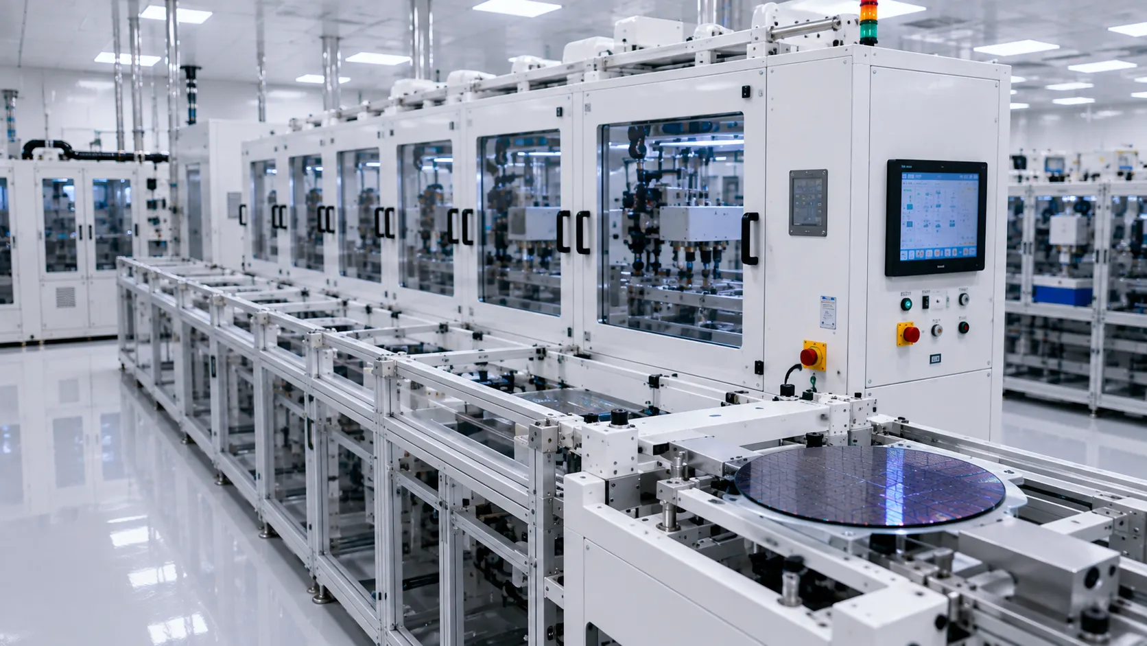
Modular Wet Bench Customization
Engineered for high chemical compatibility and versatile spatial layouts. Fully automated or semi-automated chamber architectures utilizing ultra-pure fluoropolymer construction.
- PTFE, PVDF, and PFA corrosion-resistant builds
- High-precision closed-loop thermal control
- Custom bath geometries for non-standard substrates
Specialized Cleaning & Etching Systems
Precision particle removal and chemical etching tools configured for delicate surface topographies, high-aspect-ratio features, and sensitive stack layers.
- Combined megasonic and ultrasonic agitation
- Microfluidic flow path and bath dynamics control
- Multi-tank parallel and cascade process architectures
Point-of-Use Exhaust & Scrubber Systems
Integrated gas abatement and liquid effluent treatment units built for safe handling of aggressive chemistries, toxic vapors, and hazardous process exhaust.
- Dedicated scrubbers for SiH4, NF3, and acid vapors
- Integrated chemical neutralization & dosing loops
- Real-time emission monitoring & safety interlocks
Automated Wafer Handling & Fab Integration
High-precision robotic loading and transfer systems engineered to minimize particle contamination while enabling seamless communications with factory host software.
- Equipment Front End Modules (EFEM) integration
- Custom robotic end-effectors for fragile wafers
- Native SECS/GEM interface software stack
Comprehensive Engineering Capabilities & Technology Breakdown
KOSEN SEMI operates at the forefront of semiconductor wet process customization, combining deep mechanical engineering, fluid mechanics, and software automation. Our engineering methodology delivers end-to-end customization across every critical equipment module, ensuring zero compromise on yields, uptime, or safety.
Substrate Versatility & Advanced Material Selection
Whether processing standard silicon or advanced compound materials like Silicon Carbide (SiC) and Gallium Nitride (GaN), process chambers must endure aggressive chemistries without leaching impurities. KOSEN SEMI specifies high-purity PTFE, PVDF, and PFA components to maintain pristine cleanroom standards.
- Material Compatibility: Fluoropolymer chambers withstand concentrated HF, HNO3, H2SO4, and SPM chemistry.
- Substrate Adaptability: Customized wafer boats and end-effectors handle thin, warped, or non-standard substrates.
Precision Chemical Delivery & Thermal Control
Etch rate uniformity and cleaning efficiency rely on tight chemical temperature control and fluid flow dynamics. Our custom wet benches incorporate closed-loop inline heating, rapid cooling manifolds, and active bath recirculation to prevent stagnation and boundary-layer inconsistencies.
- Thermal Stability: Inline quartz and fluoropolymer heaters maintain accurate temperatures within ±0.5°C.
- Fluid Dynamics Optimization: CFD-modeled fluid injection manifolds deliver uniform chemical distribution.
Point-of-Use Scrubber & Environmental Compliance
Effluent management is vital for fab safety and environmental compliance. KOSEN SEMI designs custom point-of-use scrubber modules tailored to specific process gas profiles and chemical drain streams, incorporating multi-stage packed towers, chemical dosing, and automated fail-safe interlocks.
- Gas & Effluent Abatement: High-efficiency treatment for silane, nitrogen trifluoride, and corrosive gases.
- SEMI Compliance: Engineered with hardware interlocks and redundant monitoring to meet SEMI S2/S8 standards.
Factory Automation & Protocol Integration
Modern fab operation requires seamless tool-to-host connectivity and particle-controlled material transfers. KOSEN SEMI equips custom equipment with automated loading mechanisms, robotic end-effectors tailored to wafer geometries, and fully compliant SECS/GEM communications.
- Robotic Handling: Multi-axis wafer transfer robots with programmable force sensors and custom grippers.
- Host Connectivity: Native SECS/GEM and GEM300 compliance for automated fab execution systems (MES).
Discuss Your Custom Equipment Requirements with Our Engineers
Partner with KOSEN SEMI to evaluate your process specifications, material compatibility requirements, and tool automation goals.
Standardized Delivery Process for Custom Semiconductor Equipment
Developing non-standard semiconductor equipment demands rigorous risk management and transparent project execution. KOSEN SEMI eliminates custom engineering risks through a disciplined, five-phase project framework that guarantees technical compliance, process reliability, and rapid fab integration. Learn more about our Engineering Capability to see how we deliver custom precision.
Requirements Assessment & Process Alignment
Our application engineers collaborate directly with your team to review substrate parameters, chemical compatibility, footprint limits, and cleanliness targets.
- Substrate sizing for 150mm, 200mm, and 300mm wafers or specialty substrates
- Corrosion-resistant material selection (PTFE, PVDF, PEEK, and quartz)
- Cleanroom footprint alignment for ISO Class 5–7 environments
Key Output: Technical Specification Matrix
3D CAD Design & Simulation
Mechanical and process engineers model tool structures in 3D and perform advanced fluid and thermal simulations to refine performance before manufacturing.
- Computational Fluid Dynamics (CFD) modeling for bath recirculation
- Thermodynamic simulation for uniform heating and temperature control
- Mechanical stress analysis and ergonomic safety modeling
Key Output: 3D Blueprint & Simulation Report
Modular Assembly & Control System Integration
High-purity sub-assemblies are built in cleanroom conditions while software engineers configure dedicated PLC control architectures and host communication protocols.
- High-purity piping and leak-tested joint assembly
- Custom PLC controller programming with intuitive HMI interfaces
- Seamless SECS/GEM protocol setup for automated fab host communication
Key Output: Integrated System Architecture
In-Plant FAT & Safety Pre-Audit
Before shipment, every custom tool undergoes Factory Acceptance Testing (FAT) in our facility, including operational dry runs and safety interlock validation.
- Full recipe sequence execution and chemical loop stress testing
- Hardware interlock, emergency shutoff (EMO), and safety checks
- Preliminary audit for SEMI S2 and SEMI S8 safety standard compliance
Key Output: Factory Acceptance Test (FAT) Report
On-Site SAT & Fab Commissioning
KOSEN SEMI deployment engineers manage cleanroom positioning, utility hookups, process qualification, and operator training for seamless tool handover.
- Precision positioning and cleanroom docking
- Facility utility connection and gas/liquid line leak checks
- On-site process qualification and recipe tuning
- Comprehensive operational and maintenance technician training
Key Output: Site Acceptance Test (SAT) Certificate
24/7 Lifetime Engineering SupportTurnkey Engineering Deliverables & Milestone Commitments
Our project governance gives semiconductor manufacturers complete clarity across every engineering phase.
| Project Phase | Technical Scope | Quality Checkpoint | Documentation Deliverable |
|---|---|---|---|
| Requirements Phase | Substrate geometry, chemical compatibility, and process specifications | Cleanroom footprint and facility utility verification | Technical Specification Matrix |
| Design Phase | 3D CAD structural modeling and CFD fluid/thermal simulation | Fluid dynamics and temperature distribution modeling | 3D Blueprint & Simulation Report |
| Assembly Phase | High-purity piping, cabinet assembly, and controller logic | Piping pressure test and leak integrity validation | Software Architecture & Manual |
| FAT Phase | Full recipe dry run and hardware interlock testing in plant | SEMI S2/S8 safety and functional pre-audit | Factory Acceptance Test (FAT) Report |
| SAT Phase | Cleanroom installation, utility hookup, and process tuning | On-site wafer process qualification and safety clearance | Site Acceptance Test (SAT) Certificate |
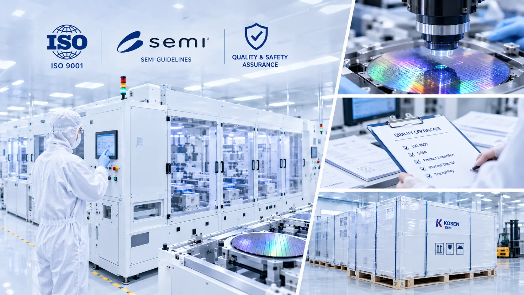
Global Quality Compliance & Safety Assurance
KOSEN SEMI adheres strictly to ISO 9001 manufacturing standards and international SEMI guidelines. Our standardized custom delivery framework mitigates non-standard tool development risks, delivering reliable, high-yield wafer processing solutions on schedule.
Standard vs. Custom Equipment: Finding the Ideal Solution
Evaluating whether off-the-shelf tools match your process goals or if non-standard engineering is required is crucial. KOSEN SEMI helps you evaluate technical specifications to select the most cost-effective machinery platform.
Standard Equipment
Best Fit When You Need:
- Standard 6", 8", or 12" silicon wafer dimensions
- Conventional RCA cleaning systems or established chemical processes
- Strict budget boundaries with delivery timeframes under 4 weeks
- Processes operating entirely within standard published parameters
Custom Equipment
Engineered For:
- Non-standard substrates and compound semiconductors (GaAs, SiC, GaN)
- Proprietary chemistry blends, aggressive acids, or specialized fluidics
- Tight, space-constrained cleanroom layouts and non-standard bay footprint limits
- Customized automation protocols, robotics, and proprietary fab SECS/GEM integration
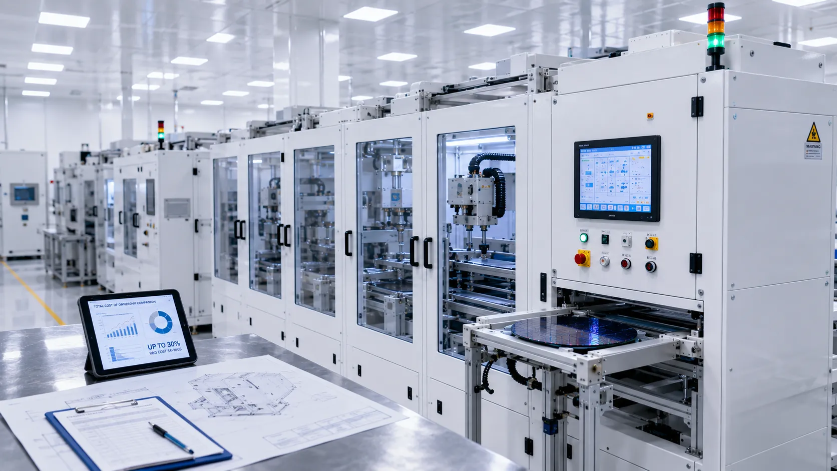
Decision Guide: Maximizing ROI with Custom Engineering
When process requirements exceed off-the-shelf specs, custom-engineered equipment eliminates costly process workarounds and lowers total R&D trial-and-error expenses by up to 30%. From targeted modifications of standard tools to complete non-standard tool development, KOSEN SEMI delivers high-ROI equipment configurations tailored to your yield goals.
| Evaluation Criteria | Standard Equipment | Custom Equipment |
|---|---|---|
| Wafer & Substrate Size Support | 6", 8", or 12" standard sizes | Any wafer diameter, thin wafer, or custom shape |
| Substrate Material Compatibility | Silicon wafers only | GaAs, SiC, GaN, Sapphire & Glass |
| Chemical & Fluidics Configuration | Standard RCA & common solvents | Fully configurable specialized chemical modules |
| Cleanroom Layout & Footprint | Fixed standard footprint | Tailored footprint & utility drop alignment |
| Automation & Host Integration | Standard SEMI communication interfaces | Custom PLC, SECS/GEM & robotic EFEM integration |
| Typical Project Timeline | Under 4 weeks standard delivery | Scoped by engineering milestones (12–24 weeks) |
Need guidance determining whether standard or custom equipment fits your target process parameters? Our application engineers are ready to evaluate your requirements.
Request a Custom Feasibility AssessmentFrequently Asked Questions About Custom Semiconductor Equipment
Addressing key technical considerations around lead times, intellectual property protection, component standardization, and SEMI safety compliance for non-standard tools.
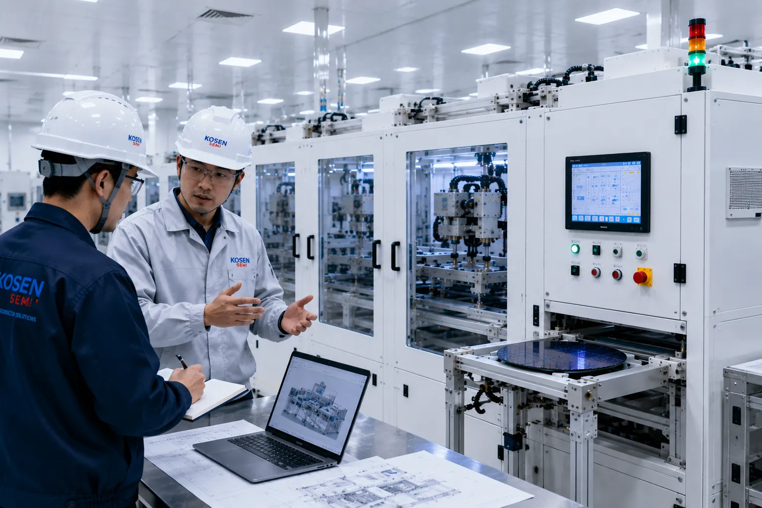
Engineering Excellence
Navigating non-standard semiconductor tool manufacturing requires experienced engineering oversight. KOSEN SEMI delivers transparent project milestones, proactive risk mitigation, and full lifecycle engineering support for fabs and R&D facilities worldwide. To learn more about our team and operational focus, visit our about-us page.
Global Field Support & Service
Our dedicated field service engineers are strategically located near major semiconductor manufacturing hubs, providing on-site SAT testing, rapid spare parts dispatch, and 24/7 technical assistance to minimize fab downtime.
What is the average lead time for custom semiconductor equipment delivery?
The average delivery cycle for custom semiconductor equipment ranges from 12 to 24 weeks, depending on architectural complexity, automation requirements, and chemical compatibility specifications. Unlike standardized off-the-shelf equipment, every custom wet bench or processing chamber undergoes systematic engineering validation.
- Process Evaluation & CFD Modeling (Weeks 1 to 4): izing substrate specifications, fluid dynamics simulations, chemical compatibility analysis, and preliminary 3D CAD design.
- Precision Manufacturing & Assembly (Weeks 5 to 14): High-precision CNC machining of corrosion-resistant polymers (PTFE, PVDF, PEEK), structural frame fabrication, and cleanroom subassembly.
- Software & Automation Integration (Weeks 12 to 18): Programmable logic controller (PLC) programming, custom HMI interface development, hardware safety interlock wiring, and SECS/GEM protocol configuration.
- In-House FAT & Pre-SEMI Inspection (Weeks 19 to 24): Rigorous Factory Acceptance Testing (FAT), chemical flow verification, sensor calibration, emergency shutoff testing, and pre-shipment sign-off.
Can we sign a Non-Disclosure Agreement (NDA) prior to sharing process specs?
Yes, absolutely. Protecting proprietary wafer processing flows and chemical formulations is fundamental to our business model. KOSEN SEMI routinely executes formal bilateral Non-Disclosure Agreements (NDAs) prior to reviewing any confidential engineering documentation, substrate dimensions, or recipe parameters.
- Strict IP Confidentiality Protocols: Engineering drawings, recipe files, and process parameters are stored in isolated, access-restricted repositories.
- 100% Client IP Ownership: Custom process chamber modifications or chemical delivery innovations developed exclusively for your application remain fully your intellectual property.
- Isolated Cleanroom Assembly: Proprietary tool builds and testing take place in secure, access-controlled manufacturing bays to prevent unauthorized exposure.
How do you ensure long-term spare parts availability for non-standard tools?
To eliminate long-term maintenance bottlenecks, KOSEN SEMI utilizes a modular engineering philosophy. While process chambers and chemical fluidic paths are custom tailored to your process, hardware interconnects, valves, sensors, and pumps incorporate standardized, high-purity components.
- Standardized High-Purity Subassemblies: Integration of top-tier commercial off-the-shelf valves, pneumatic controls, and robotic end-effectors for straightforward long-term replacement.
- Complete Asset Documentation: Every delivery includes fully serialized Bill of Materials (BOM), electrical/piping schematics, and recommended spare parts stocking lists.
- Global Stocking & Rapid Fulfillment: We maintain strategic inventories of critical wear items across major semiconductor clusters to ensure minimal replacement lead times.
Do your custom tools comply with SEMI S2, S8, and international safety standards?
Yes. Every custom tool engineered by KOSEN SEMI is built to comply strictly with international semiconductor equipment safety guidelines, including SEMI S2, SEMI S8, and SEMI S22 standards. Compliance considerations are integrated directly into initial CAD development.
- SEMI S2 Environmental Health and Safety: Integrated chemical spill containment, automated exhaust leak monitoring, seismic bracing, and emergency off (EMO) circuit integration.
- SEMI S8 Ergonomics Design: User-centric maintenance panel layouts, safe manual material handling, clear operator visibility, and optimal wafer load heights.
- Third-Party Certification Support: Complete engineering documentation and on-site support provided during third-party safety audits and cleanroom facility sign-offs.
Have Specific Engineering Questions or Unique Tool Requirements?
Discuss your non-standard substrate dimensions, specialized chemical delivery specs, or cleanroom footprint constraints directly with our senior semiconductor application engineers.