
High-Yield Wafer Fabrication Wet Process & Line Integration
As a trusted leader in semiconductor wet process solutions, KOSEN SEMI provides global wafer fabs with ultra-stable, fully automated wet processing equipment engineered to advance semiconductor wet cleaning precision, lower cost of ownership, and maximize total wafer fab yield.
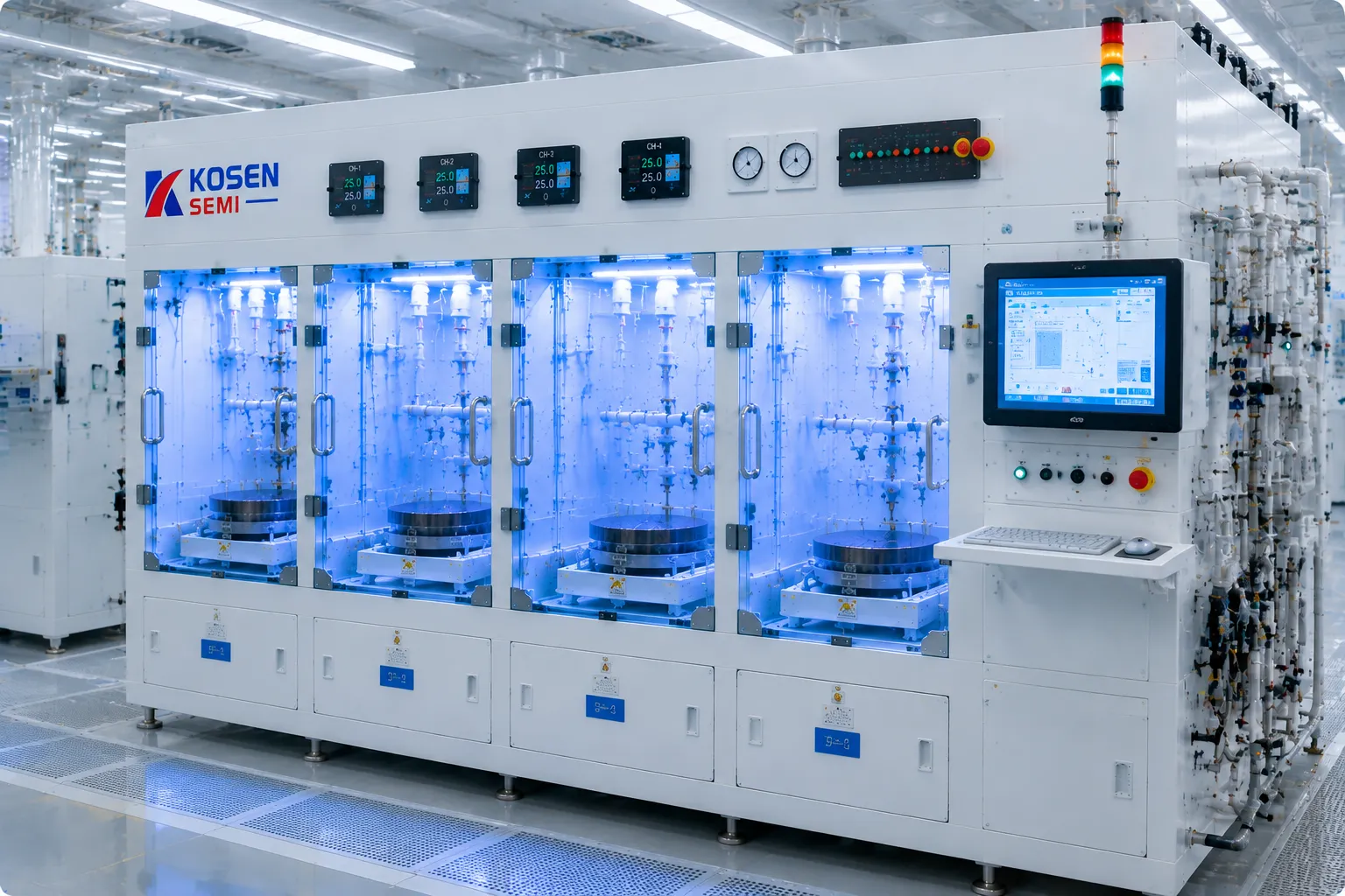
Standard Fab Automation & Protocol Integration
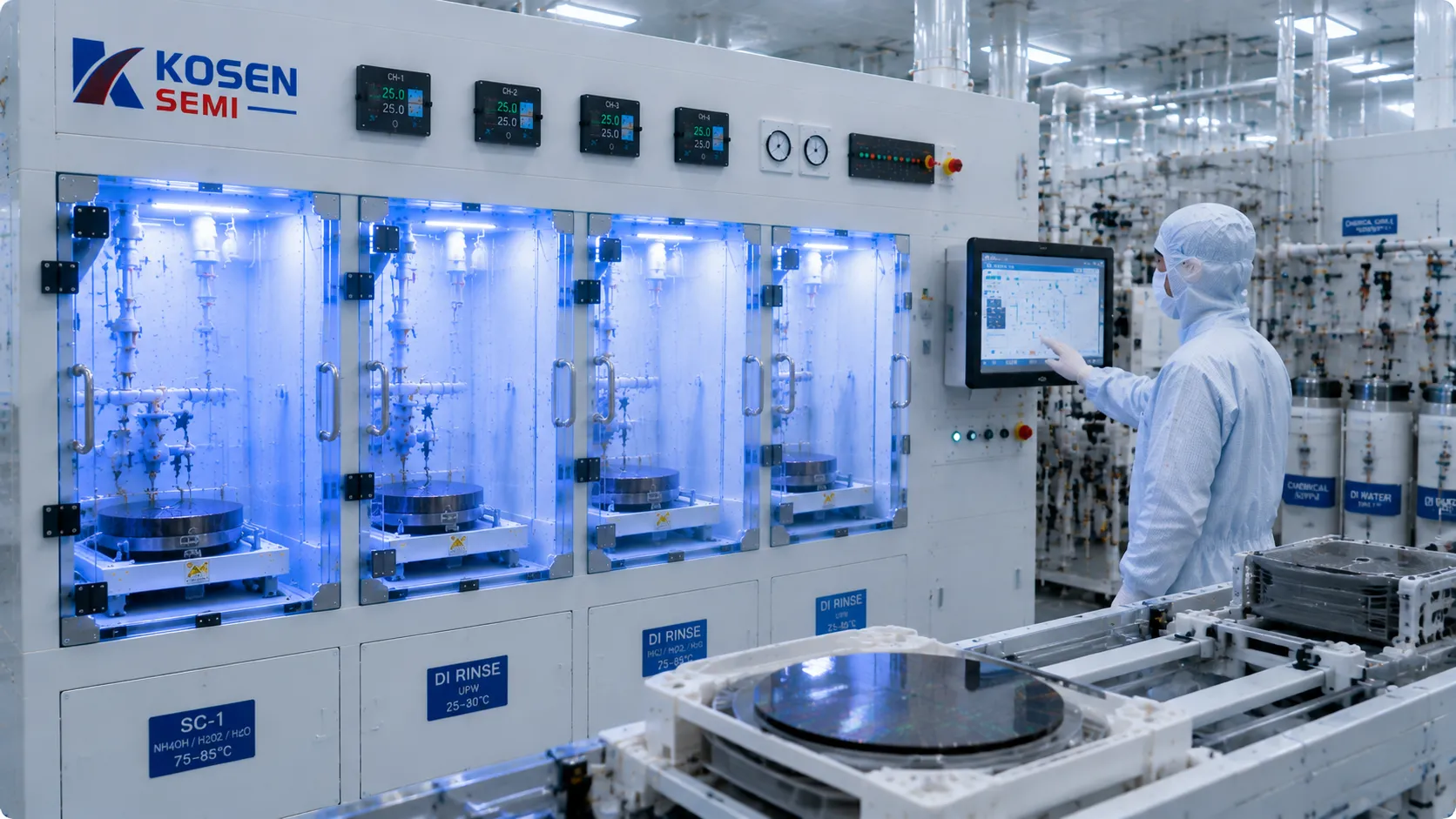
Wafer Surface Cleaning and RCA Clean Process
Substrate surface preparation prior to gate oxide growth, epitaxy, and contact formation demands atomic smoothness and near-zero impurity levels. The industry-standard RCA clean process combines Standard Clean 1 (SC-1) chemical mixing for organic film removal and micro-particle detachment with Standard Clean 2 (SC-2) chemistry for trace metallic ion extraction.
By integrating real-time chemical concentration control with non-damaging megasonic excitation, KOSEN SEMI surface cleaning tools deliver rigorous wafer contamination control. Built on our advanced Engineering Capability, this optimized fluid flow architecture eliminates the re-deposition of 200 nm-class particles, with optimized control down to 100 nm without causing structural damage to sensitive 3D feature profiles. Discover our complete line of wafer-cleaning-systems designed for high-yield semiconductor fabrication.
- Target Contaminants: Organic films, surface oxides, fine particles (standard control to 200 nm; optimized processes to 100 nm), trace metals (Fe, Cu, Ni)
- Particle Efficiency: Process-dependent particle removal performance at 200 nm, with optimized configurations targeting particles down to 100 nm
- Chemical Chemistry: SC-1 (NH₄OH/H₂O₂), SC-2 (HCl/H₂O₂), Dilute Hydrofluoric Acid (DHF), DIO3
- Tool Architecture: Recirculating quartz baths with multi-frequency megasonic transducers and continuous inline filtration
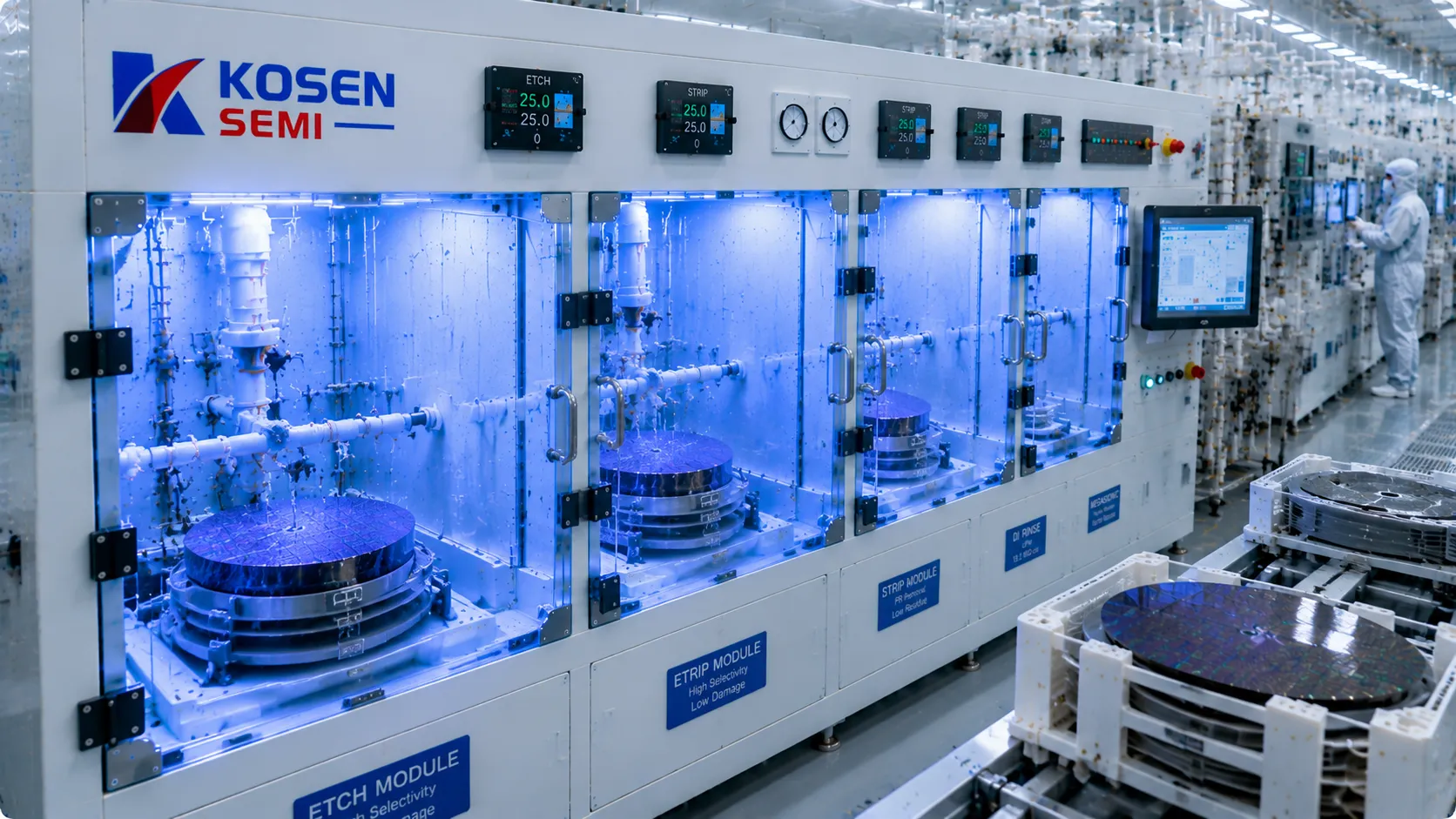
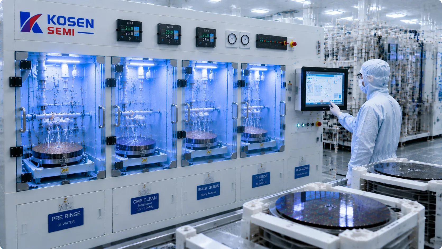
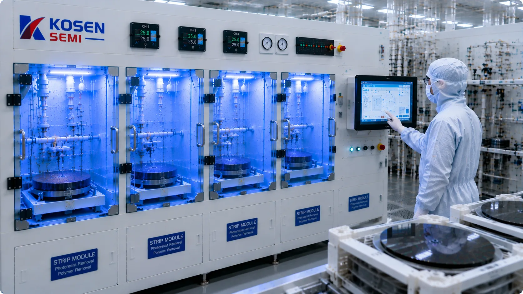
Core Wet Equipment Technology & Inline Wet Process Tools
KOSEN SEMI engineers advanced chemical delivery systems alongside high-precision wet etch and clean equipment engineered for continuous 300mm automated fab operations.
Precision Chemical Delivery
Closed-loop concentration monitoring, dynamic spiking, and automated multi-chemical blending systems that guarantee bath stability.
- Metering Method Closed-Loop Real-Time
- Chemical Blending Multi-Chemical Dynamic
- Dosing Control Automated Precision
Megasonic Cleaning Integration
Uniform megasonic acoustic fields eliminate particles down to 100 nm under optimized process conditions without cavitation damage or fragile pattern collapse in advanced Single Wafer Cleaning Systems.
- Energy Field Uniform Megasonic
- Particle Removal 200 nm Standard / 100 nm Optimized
- Pattern Safety Zero Collapse
IPA & Marangoni Drying
Zero-watermark surface drying technology engineered specifically for advanced high-aspect-ratio trench architectures.
- Surface Defectivity Zero Watermark
- Trench Capability High Aspect Ratio
- Solvent Efficiency Ultra-Low IPA
MES & SECS/GEM Line Integration
Full Industry 4.0 architecture providing real-time sensor telemetry, bath lifetime tracking, and 100% wafer lot history.
- Protocol Standard SECS/GEM Compliance
- Bath Monitoring Real-Time Telemetry
- Wafer Tracking 100% Lot History
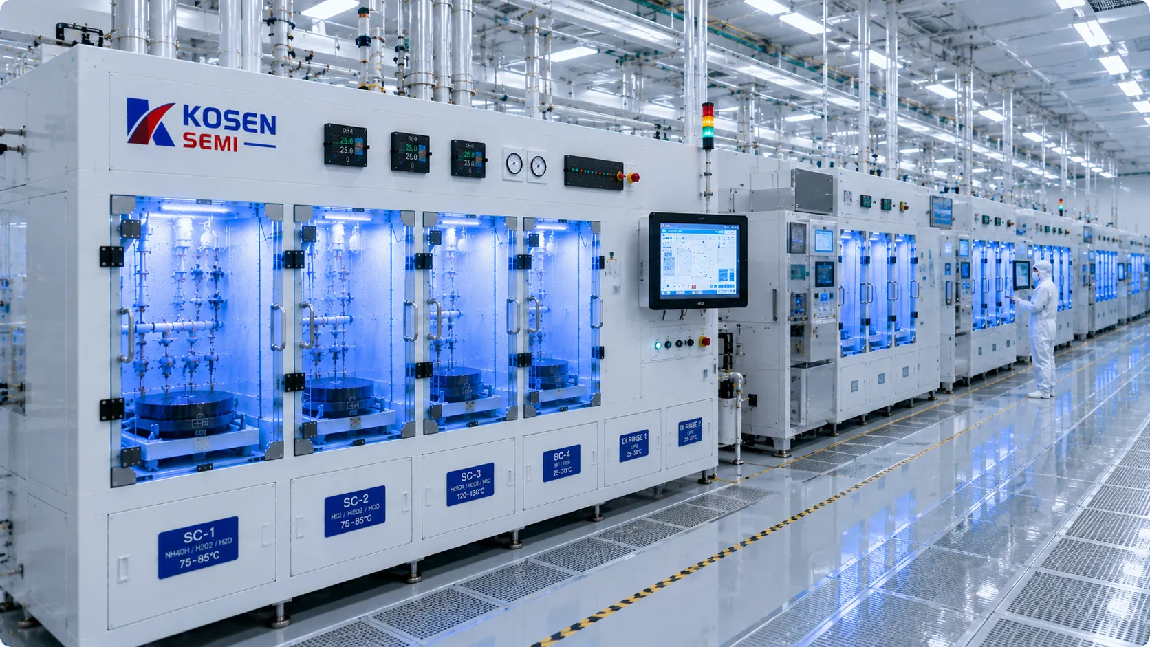
Automated 300mm Wet Process Infrastructure
Integrated inline wet process tools designed for continuous production, stringent chemical control, and maximized yield across modern wafer fabrication facilities.
Performance Benchmarking
Wafer Fab Efficiency & Yield Metrics: Legacy vs. KOSEN SEMI Integration
Un-integrated legacy wet bench setups present significant operational risks—ranging from bath chemical drift and particle contamination to excessive chemical waste and unplanned downtime—that directly degrade wafer fab efficiency and overall profitability. KOSEN SEMI's fully automated wet processing platforms eliminate these points through closed-loop chemical dosing, advanced robotic transfer, and inline telemetry. Learn more about-us and our commitment to advanced semiconductor tool designs. The result is measurable, validated operational gains that accelerate semiconductor fab yield optimization and maximize net revenue per wafer start.
Head-to-Head Wet Bench Performance Comparison
Direct benchmark metrics across key fab operations
| Evaluation Dimension | Legacy / Un-Integrated Setup | KOSEN SEMI Integrated Solution |
|---|---|---|
| Wafer Cross-Contamination Rate | High Risk — Manual bath changeovers & ambient exposure | Near-Zero — Closed-loop isolation & automated flushing |
| Chemical Consumption Volume | Unoptimized Baseline — Time-based bath dumps & waste | Up to 30% Savings — Real-time concentration spiked delivery |
| Mean Time Between Failures (MTBF) | Low MTBF — Reactive maintenance & unmonitored wear | 2× MTBF Improvement — Predictive sensor telemetry |
| Process Repeatability (Cpk) | Cpk < 1.33 — Bath chemical & thermal drift | Cpk ≥ 1.67 — Automated recipe enforcement & closed-loop dosing |
| Wafer Breakage Rate | Present Risk — Manual cassette transfer & mechanical stress | Zero Breakage Target — Integrated EFEM robotic handling |
| Overall Equipment Effectiveness (OEE) | 60–70% — Frequent unscheduled downtime & idle queues | 85–92% — SECS/GEM MES integration & dynamic dispatching |
OEE Improvement Breakdown
Overall Equipment Effectiveness gains in KOSEN SEMI integrated wet benches stem from three compounding engineering drivers: maximized system availability through predictive health monitoring, optimized performance via automated lot scheduling, and superior die yield through precise contamination control.
Automated chemical bath lifetime monitoring and predictive spiking alerts cut unscheduled downtime by up to 40%, keeping high-volume wet benches continuously online.
Full SECS/GEM and MES line integration streamlines lot transitions, eliminating idle buffer delays and delivering sustained throughput enhancement across critical FEOL and BEOL flows.
Closed-loop chemical concentration control and 200 nm particle filtration, with optimized configurations available down to 100 nm, maintain Cpk values above 1.67, drastically reducing rework and scrap rates during semiconductor fab yield optimization.
Combined chemical savings, reduced wafer scrap, and elevated tool availability enable full capital recovery within 18 to 24 months for 200mm and 300mm fabrication lines.
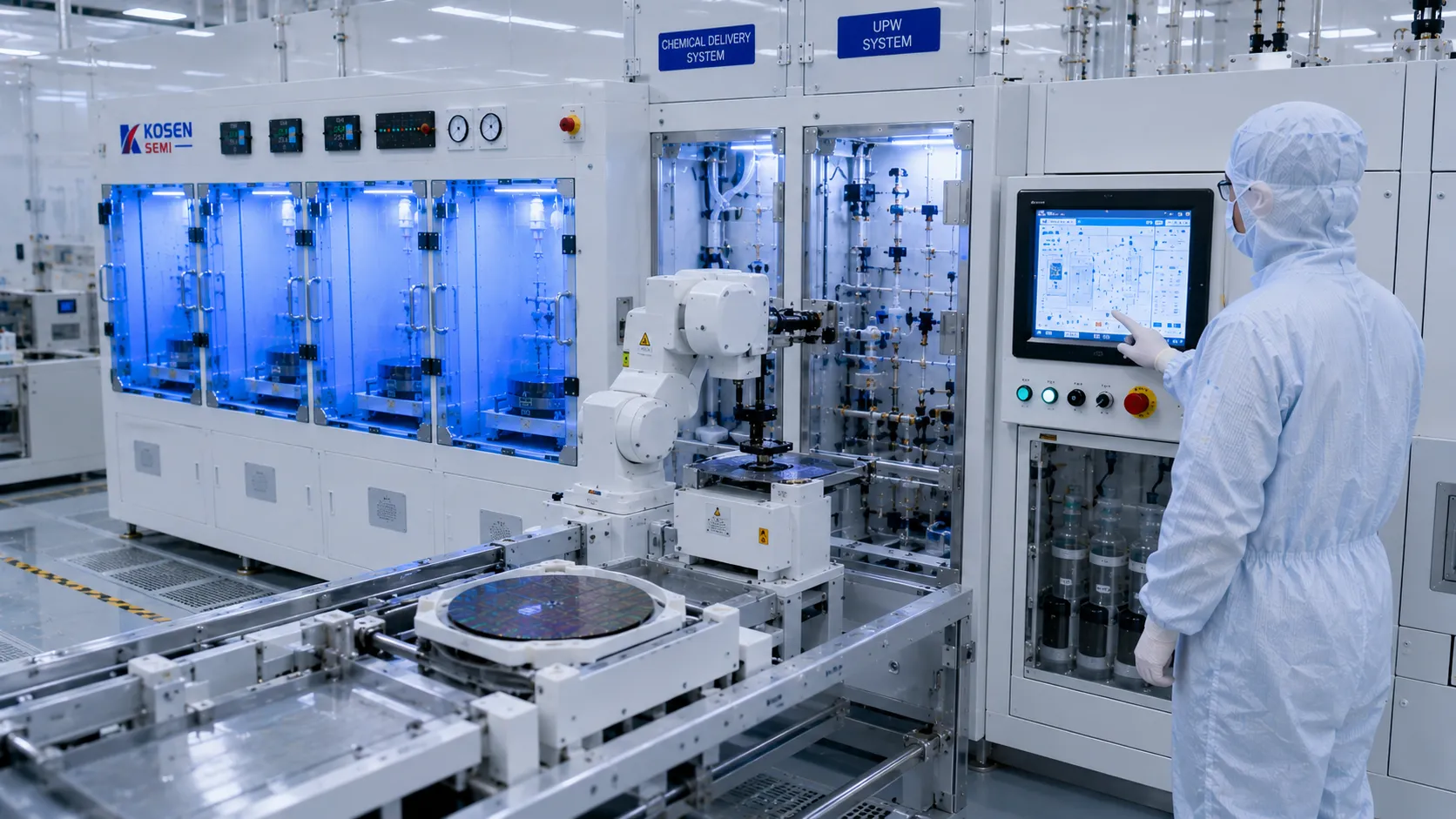
Cleanroom-ready automated wafer transfer & chemical management module.
Interactive ROI & Cost Savings Calculator
Adjust your monthly wafer starts to project annual chemical cost savings realized through KOSEN SEMI integrated wet processing technology.
Projected Savings Breakdown
Estimates based on validated production fab benchmarking across 200mm and 300mm lines. Actual results vary by chemical selection, process node, and facility utilization.
Why Semiconductor Fab Yield Optimization Starts at the Wet Bench
In modern semiconductor manufacturing, wet processing is far more than a routine surface preparation step—it is a primary determinant of final device yield. Every RCA clean cycle, wet etch pass, and post-CMP rinse directly impacts substrate micro-roughness, pattern fidelity, and defect density. Uncontrolled chemical bath depletion, bath temperature fluctuations, and manual wafer handling introduce systematic variability that compounds across hundreds of processing steps, severely impairing wafer fab efficiency.
KOSEN SEMI addresses these critical challenges directly at the hardware and software integration level. Our automated wet processing platforms, including specialized Single Wafer Cleaning Systems, feature closed-loop chemical delivery systems that maintain solution concentrations within tight tolerances of ±0.1%. Integrated megasonic cleaning modules remove particulate contaminants at 200 nm, with optimized process capability down to 100 nm without causing pattern damage to delicate high-aspect-ratio structures. Meanwhile, SECS/GEM compliance ensures seamless factory automation and full lot traceability across every production run.
Validated across high-volume 200mm and 300mm wafer fabs, KOSEN SEMI integrated wet bench solutions empower semiconductor manufacturers to accelerate process ramp-up, lower total cost of ownership (TCO), and achieve consistent throughput enhancement. By partnering with KOSEN SEMI, fabs transform wet processing into a predictable competitive advantage for long-term semiconductor fab yield optimization.
Wafer Fab Wet Process Integration and Compliance FAQ
Selecting high-yield wet processing equipment requires authoritative clarity on substrate compatibility, material purity, and automated factory integration. KOSEN SEMI delivers high-precision cleanroom wet equipment engineered to meet stringent ISO Class 5–7 cleanliness and SEMI compliance standards. Below are direct, engineering-backed answers to critical technical and procurement questions.
Hybrid Line Capability for 200mm and 300mm Wafers
Do your wet process systems support hybrid lines running both 200mm and 300mm wafers?
Hybrid Line Capability for 200mm and 300mm Wafers
Do your wet process systems support hybrid lines running both 200mm and 300mm wafers?
Yes. KOSEN SEMI engineers versatile bridge-tool configurations designed specifically for high-mix semiconductor manufacturing environments. Our systems seamlessly handle both 200mm (8-inch) and 300mm (12-inch) wafer diameters with minimal hardware changeover and zero loss in chemical delivery accuracy.
- Rapid Carrier Conversion: Modular end-effectors and adjustable load ports accommodate quick transitions between 200mm cassettes and 300mm FOUP or MAC open carriers.
- Adaptive Robotic Chucks: Multi-point non-contact or edge-grip chucks automatically calibrate clamping pressure and pitch for silicon, SiC, and GaAs wafers.
- Dynamic Fluid Hydraulics: Dedicated process software adjusts chemical flow velocity and tank bath recirculation rates according to the loaded wafer surface area.
- Universal Recipe Management: Integrated controls store pre-validated dual-diameter recipes to prevent manual calibration errors during product line shifts.
Deploying our custom wet bench solution allows fab operators to maximize existing cleanroom footprints, protecting capital investment while retaining complete agility for future yield scaling. For single-substrate processing needs, explore our specialized Single Wafer Cleaning Systems.
Chemical Resistance and Cleanroom Equipment Durability
How is chemical resistance and cleanliness maintained during continuous exposure to aggressive chemicals?
Chemical Resistance and Cleanroom Equipment Durability
How is chemical resistance and cleanliness maintained during continuous exposure to aggressive chemicals?
Sustaining process purity under continuous exposure to concentrated acids, solvents, and alkalis demands ultra-high-purity fluoropolymer construction. KOSEN SEMI utilizes premium-grade virgin materials and stringent air filtration architectures to eliminate bath contamination and structural degradation across our complete line of advanced wafer-cleaning-systems.
- Fluoropolymer Fluid Paths: All wetted piping, valves, and manifold manifolds utilize ultra-pure PFA and PTFE to eliminate trace metallic ion contamination.
- Fused Quartz Tanks: High-temperature acid etch and RCA clean baths feature flame-polished, high-purity quartz vessels resistant to thermal stress and chemical attack.
- ISO Class 5–7 Air Management: Top-mounted Fan Filter Units (FFUs) with ULPA filters maintain continuous vertical laminar airflow across active process zones.
- Positive-Pressure Enclosures: Sensitive electrical components and controls reside inside N2-purged, sealed cabinet compartments to prevent chemical vapor ingress.
This uncompromising material specification guarantees our cleanroom wet equipment delivers exceptional tool MTBF and maximum uptime across demanding FEOL and BEOL chemical processing.
Native SECS/GEM Protocol and MES Integration
Can your SECS/GEM interface integrate into our existing fab MES platform without custom middleware?
Native SECS/GEM Protocol and MES Integration
Can your SECS/GEM interface integrate into our existing fab MES platform without custom middleware?
Yes. KOSEN SEMI wet processing systems feature fully native SECS/GEM communications standards, enabling seamless, direct integration with your existing Manufacturing Execution System (MES) and automated cell controllers without third-party translation software.
- SEMI E4 (SECS-I): Establishes robust, low-level serial communication protocols for hardware-level data transfers.
- SEMI E5 (SECS-II): Defines structured message formats for real-time process monitoring, alarm propagation, and recipe management.
- SEMI E30 (GEM): Implements standardized equipment behavior models, remote state control, and comprehensive event logging.
- SEMI E37 (HSMS): High-speed TCP/IP network protocol providing rapid, reliable data exchange with host fab servers.
Our robust wafer fab process integration delivers total wafer lot traceability, real-time bath chemistry logging, and automated fault detection for total line transparency.
Project Lead Time and Qualification Timeline
What is the typical lead time from process recipe verification in the lab to full cleanroom installation?
Project Lead Time and Qualification Timeline
What is the typical lead time from process recipe verification in the lab to full cleanroom installation?
KOSEN SEMI executes tool delivery through a phased, fully transparent project roadmap to ensure fast qualification and predictable production ramp times. Standard lead times typically range from 16 to 24 weeks depending on tool customization and automation scope. Learn more about our technical focus and design expertise on our Engineering Capability page.
- Lab Recipe Verification: Collaborative chemical process testing and baseline etch/clean validation inside our ISO Class 5–7 demonstration facilities.
- Precision Modular Assembly: Custom frame fabrication, PFA tube bending, cabinet wiring, and automated chemical delivery system integration.
- Factory Acceptance Testing (FAT): Comprehensive pre-shipment dry runs, pressure vessel leak testing, chemical dosing calibration, and safety interlock verification.
- Installation and SAT: On-site cleanroom positioning, hookup connection, Site Acceptance Testing (SAT), and host MES interface sign-off.
KOSEN SEMI's dedicated field application team provides end-to-end technical support from initial process recipe validation through full volume production startup.
Expert Technical Consultation and Custom Tooling Support
Need custom chemical compatibility data, CAD footprint models, or specialized enclosure dimensions for your cleanroom facility? Speak directly with a KOSEN SEMI wet process integration engineer today.