
High-Throughput Batch Wafer Cleaning Systems for Semiconductor Fabs
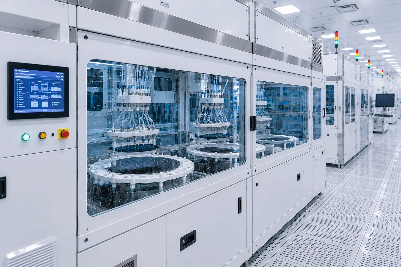
Engineered for 200mm and 300mm silicon and compound wafer manufacturing, KOSEN SEMI batch wet benches deliver >99.5% particle removal efficiency, precise chemical temperature control, and a significantly lower cost of ownership (CoO) across our advanced wafer-cleaning-systems.
Why Choose Batch Wafer Cleaning Systems for High-Volume Production?
When evaluating batch versus Single Wafer Cleaning Systems for commercial semiconductor fabs, batch wet benches deliver unmatched operational economy and throughput. KOSEN SEMI provides advanced wafer-cleaning-systems that achieve particle removal efficiency above 99.5% while reducing chemical consumption by up to 30%. Maximize your high-throughput cleaning capacity while significantly lowering your overall wet cleaning cost of ownership.
Maximum Throughput Capacity
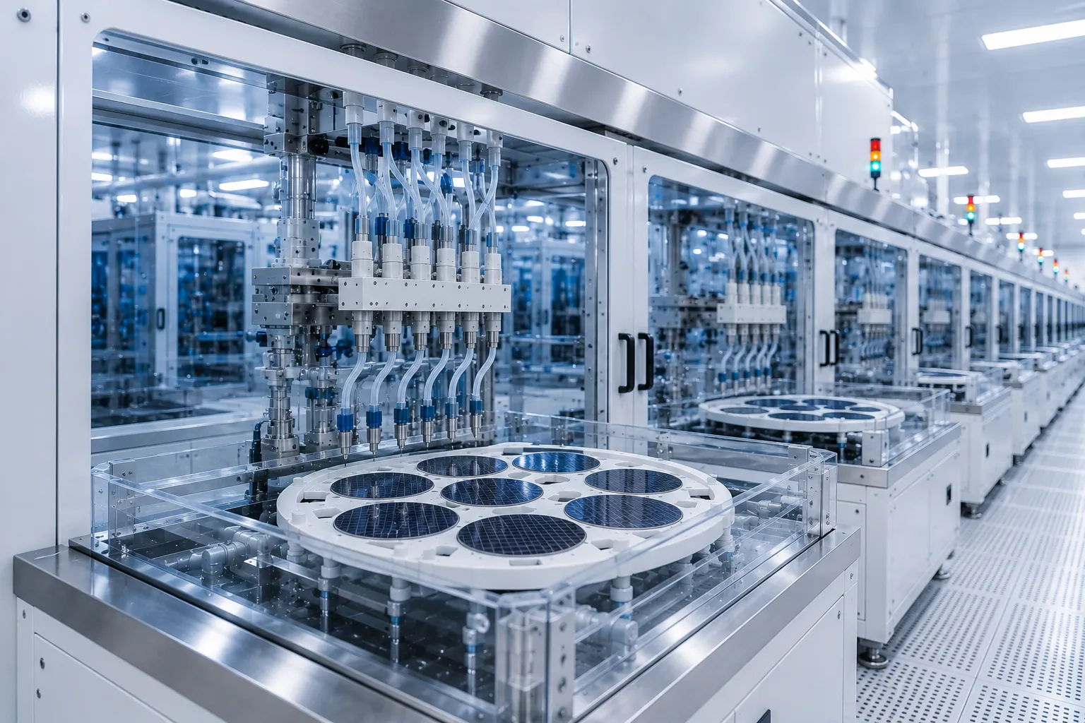
Engineered with high-capacity chemical baths for continuous 200mm and 300mm wafer processing, maximizing overall fab output.
Optimized Chemical Consumption
Recirculating filtration and automated chemical management slash raw fluid consumption and drastically lower your total cost of ownership.
Multi-Tank Temp & Megasonic Control
Integrated multi-frequency megasonic transducers paired with closed-loop thermal regulation deliver uniform particle removal at 200 nm standard capability, optimized down to 100 nm.
Substrate Damage Protection
High-precision servo robotic handling and anti-scratch cassette fixtures protect delicate micro-structures and reduce breakage risk.
Precision Wet Chemical Processing and Advanced Drying Architecture
KOSEN SEMI batch wafer cleaning systems combine modular chemical bath engineering with advanced acoustic energy delivery and surface-tension-driven drying. Built for high-volume 200mm and 300mm semiconductor fabrication, our custom Engineering Capability allows us to tailor chemical wet bench platforms that support 200 nm standard contaminant removal, optimized down to 100 nm while optimizing chemical consumption across complex device architectures. In addition to batch systems, we provide advanced Single Wafer Cleaning Systems to meet diverse process requirements.
Ultra-Pure Bath Construction & Chemical Process Compatibility
Continuous exposure to aggressive acids and bases demands stringent material purity and thermal stability. KOSEN SEMI chemical wet benches utilize high-grade quartz and virgin PTFE/PFA Teflon bath construction, preventing ionic contamination and chemical leaching during intensive wafer processing cycles.
Flame-polished, semiconductor-grade quartz tanks optimized for high-temperature SPM (sulfuric-peroxide) and SC1/SC2 cleaning up to 150°C with indirect immersion heating.
Seamlessly molded PTFE/PFA tanks designed specifically for oxide etching and surface passivation, minimizing the risk of chemical leaching or material degradation.
Key Technical Highlights
- ✓ Recirculating Chemical Filtration: Integrated sub-0.05 µm point-of-use filters continuously remove bath micro-particulates.
- ✓ Automated Chemical Spiking: Closed-loop volumetric dosing maintains precise chemical ratios over extended production shifts.
- ✓ Thermal Precision Jackets: Double-walled bath isolation limits thermal dissipation and preserves ±0.1°C temperature uniformity.
- ✓ Configurable Multi-Tank Layouts: Flexible configurations accommodating 4 to 8 active chemical baths and quick-dump rinse (QDR) modules.
High-Throughput Wet Cleaning Across Semiconductor & Advanced Substrate Lines
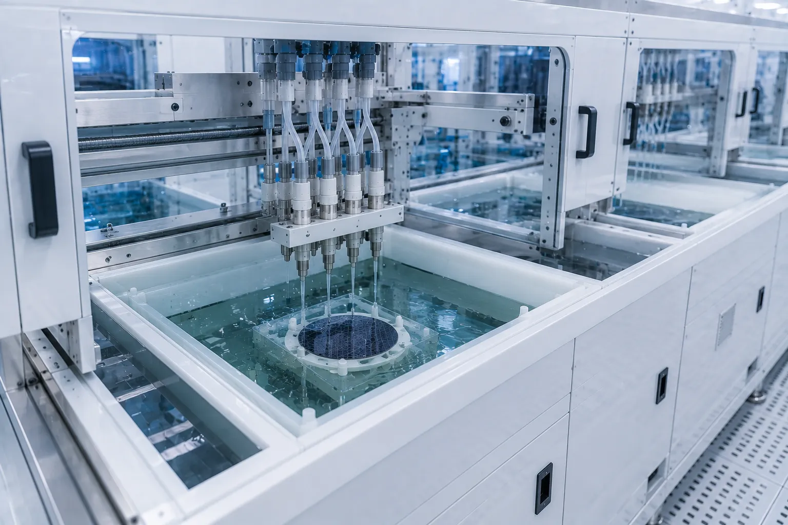
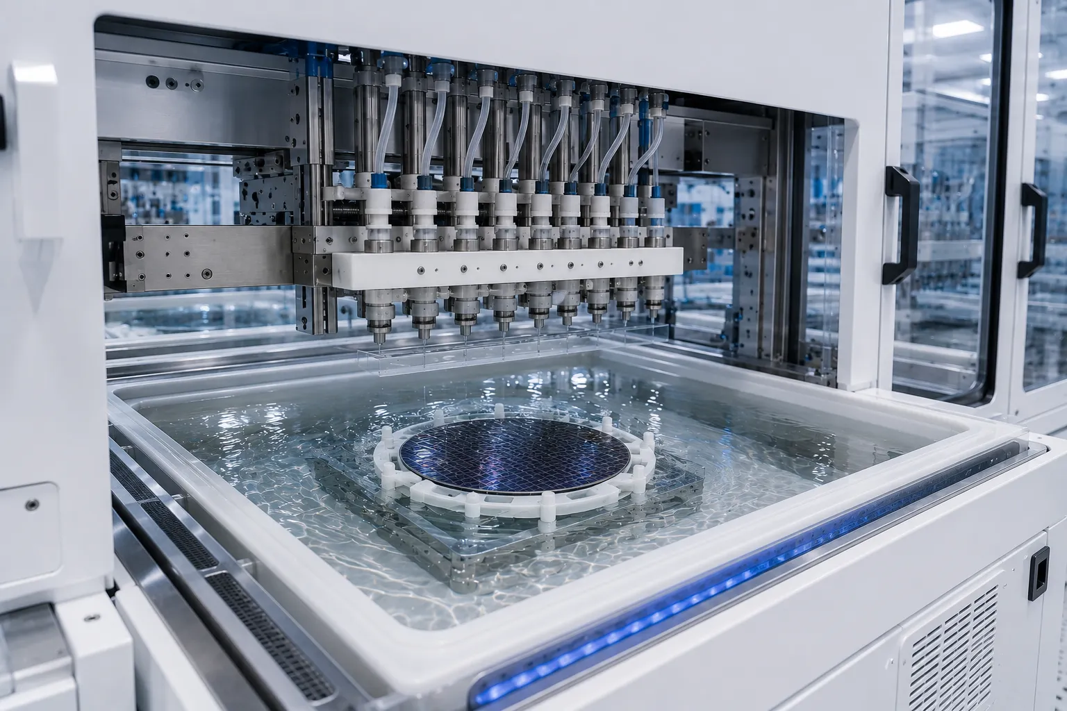
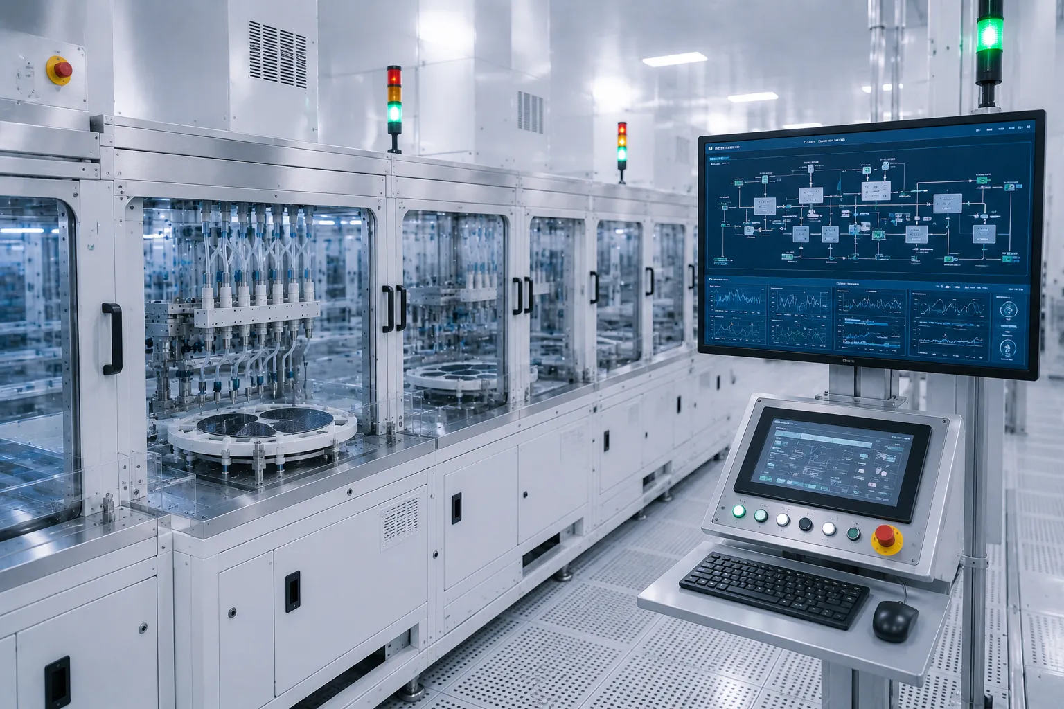
Semiconductor wet processing demands rigorous chemical bath control, 200 nm standard particulate removal, optimized down to 100 nm, and damage-free wafer handling tailored to specific crystal orientations and fab workflows. KOSEN SEMI batch wafer cleaning systems deliver exceptional contamination control across front-end silicon IC fabrication, wide-bandgap compound semiconductors, 3D advanced packaging, and precision optoelectronic device manufacturing.
Designed for demanding front-end wafer cleaning (FEOL) and back-end yield optimization (BEOL), our modular chemical wet benches seamlessly integrate into 150mm, 200mm, and 300mm substrate production lines. By controlling fluid dynamics, bath temperature uniformity, and megasonic energy distribution, KOSEN SEMI equipment ensures repeatable surface preparation for delicate micro-structures.
 Silicon & Logic Fabrication
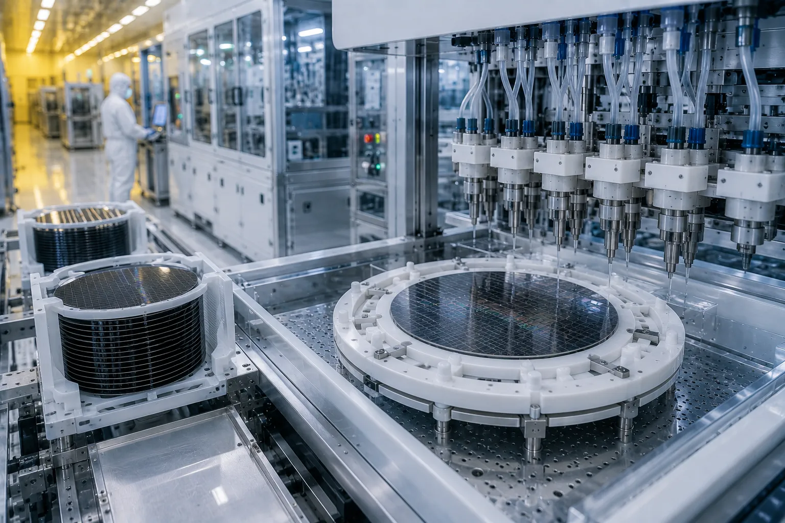
 Silicon Wafer Fabrication & Post-CMP Cleaning
High-volume silicon IC fabrication requires continuous micro-contamination removal across raw wafer manufacturing and device patterning. KOSEN SEMI batch systems deliver rapid organic residue stripping, metallic impurity removal, and particle elimination required for ingot slicing cleanup, gate oxide formation, and post-chemical mechanical planarization (Post-CMP), complementing our advanced Single Wafer Cleaning Systems.
- Post-CMP Cleaning: Removes slurry particulates at 200 nm standard capability, optimized down to 100 nm without etching underlying dielectric or metal layers.
- FEOL Surface Processing: Multi-bath RCA (SC1/SC2) chemical sequences optimized for ultra-thin gate oxide integrity.
- Ingot Slicing & Substrate Prep: High-throughput slurry and kerf residue removal for raw 200mm and 300mm silicon wafers.
 Power & RF Semiconductors
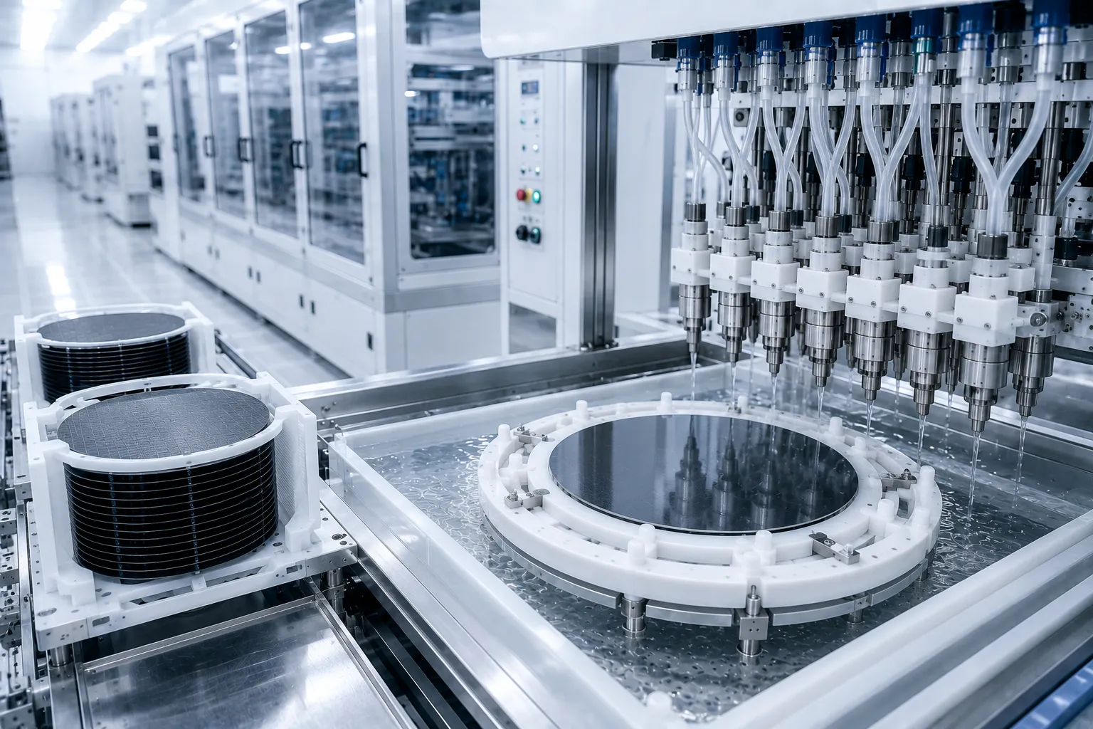
 Compound Semiconductors (SiC & GaN Substrates)
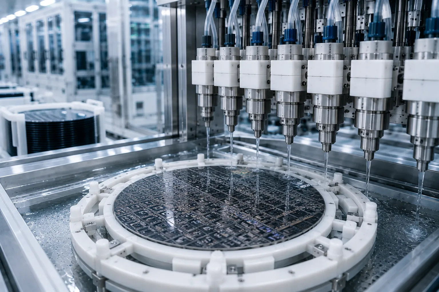
Third-generation wide-bandgap materials like Silicon Carbide (SiC) and Gallium Nitride (GaN) present tough chemical resistance and extreme surface hardness challenges. KOSEN SEMI SiC wafer cleaning equipment removes stubborn native oxides and mechanical polish contaminants to prepare substrate surfaces for low-defect epitaxial layer growth.
- Substrate Surface Conditioning: Chemically assisted surface preparation engineered specifically for chemical-resistant SiC/GaN wafers.
- Pre-Epitaxial Cleaning: Targets trace metallic contaminants at validated detection limits to prevent lattice defects in epi-layers.
- Megasonic Particle Stripping: Uniform megasonic cavitation dislodges particles at 200 nm standard capability, optimized down to 100 nm without causing crystal lattice damage.
 3D Packaging & MEMS
 Advanced Packaging & MEMS Micro-Structures
Modern 3D IC architectures, Through-Silicon Vias (TSVs), and MEMS sensors feature deep aspect ratios and fragile mechanical features highly susceptible to pattern collapse. KOSEN SEMI wet processing systems combine gentled chemical agitation and controlled megasonic power to clear deep trenches without damaging fragile micro-structures.
- TSV Sidewall & Cavity Cleaning: Penetrates high-aspect-ratio vias to completely strip residual polymer and photoresist.
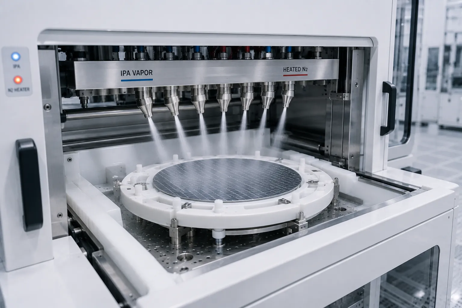
- Marangoni IPA Vapor Drying: Supports low-watermark drying inside microscopic cavities and narrow trench structures.
- Non-Contact Robotic Transfer: High-precision servo arm robotics and non-edge-touch cassette clamping prevent wafer breakage.
 Photonics & Optoelectronics
 Photovoltaic & Optoelectronic Devices
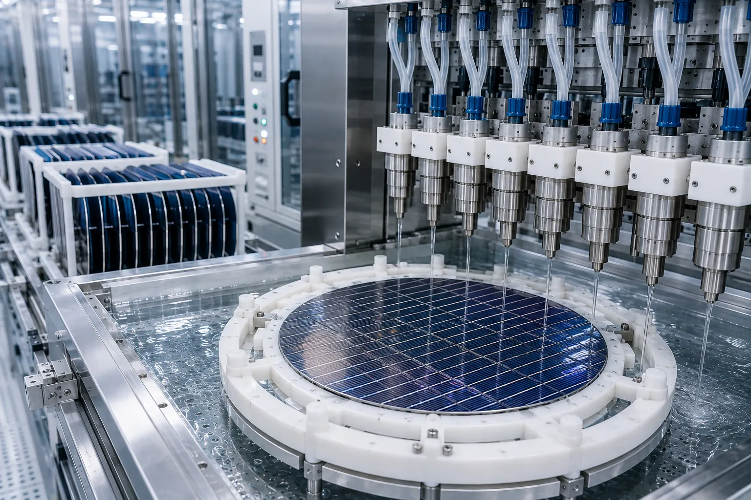
High-efficiency solar cells, laser diodes, and optical sensors demand precise chemical texturing and defect-free surface preparation. Our batch silicon wafer wet processing solutions deliver controlled surface modification, chemical polishing, and contamination removal across large-scale optoelectronic substrate manufacturing lines.
- Precision Chemical Texturing: Closed-loop temperature control supports uniform alkaline or acidic pyramid formation.
- Cross-Contamination Suppression: High-efficiency quick-dump rinse (QDR) baths reduce chemical drag-out between process steps.
- Cost of Ownership Optimization: Continuous chemical recirculation and filtration dramatically reduce bath chemical consumption.
Custom Wet Bench Process Recipes Tailored to Your Fab Workflow
From high-volume 300mm silicon fabs to specialized wide-bandgap SiC/GaN foundries, KOSEN SEMI provides customized wet bench process recipes tailored to exact process integration needs. Backed by our robust Engineering Capability, our application engineers partner with your process teams to optimize chemical immersion times, megasonic energy profiles, and Marangoni drying parameters for maximum die yield.
Whether upgrading a 200mm legacy line or equipping a fully automated 300mm smart fab with SECS/GEM integration, our modular batch wafer cleaning systems deliver the process flexibility, low chemical CoO, and continuous reliability modern semiconductor manufacturing demands.
Batch Wafer Cleaning System Specifications & Matrix
Compare key engineering parameters across 150mm, 200mm, and 300mm batch wet benches. KOSEN SEMI delivers high wafer cleaning throughput, 200 nm standard particle removal, optimized down to 100 nm, and fully customizable chemical bath configurations.
| Technical Parameter | 150mm / 200mm Configuration | 300mm Batch Wet Bench | Modular Expansion Options |
|---|---|---|---|
| Supported Wafer Diameters | 150 mm / 200 mm (Si, SiC, GaN) | 300 mm (Silicon & Advanced Substrates) | Dual-diameter combi carriers & custom end-effectors |
| Batch Processing Capacity | Up to 25 Wafers per batch | Up to 50 Wafers per batch | High-density carriers & continuous automation transfer |
| Chemical Tank Range | 4 – 6 Process Baths (RCA, HF, SPM) | 6 – 8 Dedicated Process Tanks | Expandable inline bath modules & auto chemical spiked dosing |
| Particle Removal Efficiency (PRE) | PRE > 99.5% (200 nm Standard) | PRE > 99.5% (100 nm Optimized) | Multi-frequency megasonic & Marangoni IPA drying |
| Cleanroom Environment Rating | ISO Class 5–7 | ISO Class 5–7 | Enclosed mini-environment with ULPA filtration hood |
| Fab Automation & SECS/GEM | Fully Integrated SECS/GEM | SECS/GEM 300mm Suite (E30, E37, E87, E94) | Custom MES host interface & real-time telemetry |
All KOSEN SEMI batch wet benches support seamless integration with factory MES via standard SECS/GEM protocols for fully automated wafer processing. For single-wafer processing needs, explore our advanced Single Wafer Cleaning Systems.
Our modular engineering architecture allows tailored chemical bath staging, robotic transfer retrofits, and scalable wafer cleaning throughput for high-volume fabs.
Require detailed semiconductor cleaning equipment specifications?
Request engineering datasheets, chemical compatibility matrices, and facility layout schematics for your fab team.
Built to Rigorous Global Standards for Semiconductor Manufacturing
Every KOSEN SEMI wet bench completes over 100 continuous hours of cleanroom verification prior to final customer acceptance. We engineer premium ISO cleanroom semiconductor equipment, including advanced wafer-cleaning-systems, designed for maximal semiconductor equipment reliability and design alignment with SEMI S2 guidelines in high-volume fabs.
Mitigate procurement risks with fully documented EHS safety compliance, ultra-clean assembly protocols from our state-of-the-art manufacturing-facility, and internationally accredited quality certifications.
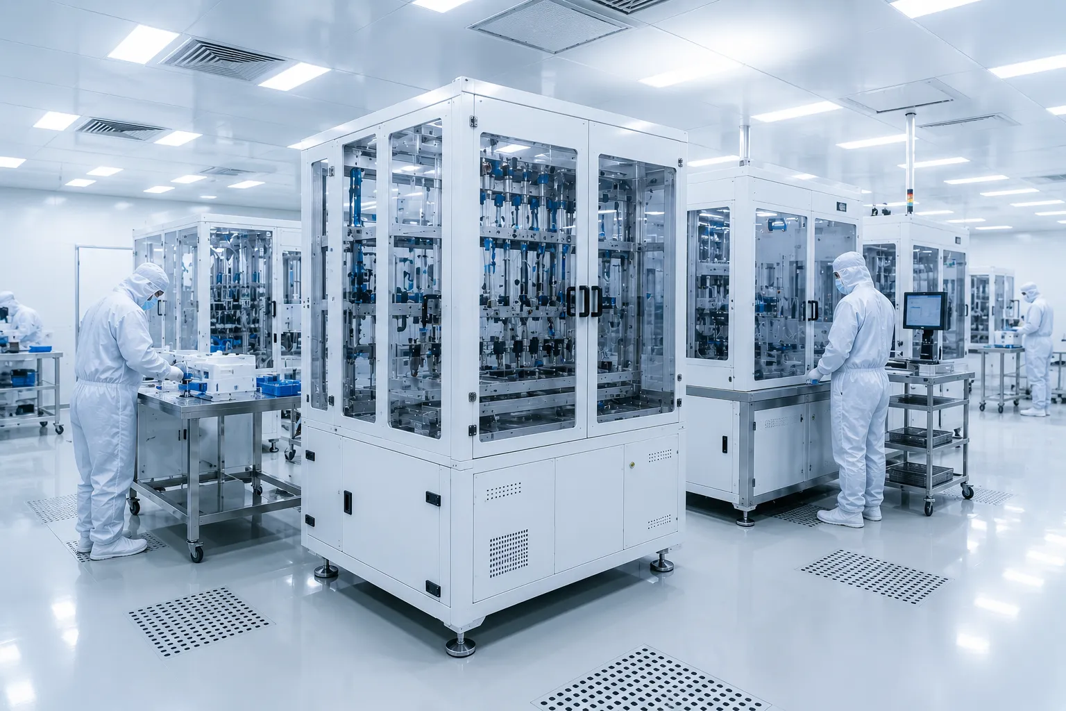
Strict environmental controls reduce airborne micro-contaminants during tool assembly and validation.
Inspect Official Compliance Documentation
SEMI S2 / S8 Compliance
Verified environmental, health, and ergonomics standards for seamless SEMI S2 compliant wet bench integration.
ISO 9001 & 14001
Certified quality controls and environmental systems supporting consistent process repeatability.
ISO Class 5–7 Build
Precision assembly backed by high-level Engineering Capability inside controlled cleanroom environments prevents initial particle introduction.
Global 24/7 Field Service
Dedicated Field Service Engineers (FSE) and fast-response technical support for uninterrupted fab production.
100+ Hour Testing
Continuous operational validation prior to Factory Acceptance Testing (FAT) ensures high tool reliability.
Frequently Asked Questions: Batch Wafer Cleaning Systems
Expert answers to technical inquiries regarding tool selection, chemical bath compatibility, preventive maintenance schedules, and fab automation integration.
How do I choose between Batch Wafer Cleaning and Single Wafer Cleaning for my line?
Selecting between a batch wafer cleaning systems setup and a single-wafer processing tool depends primarily on target throughput requirements, defect density limits, chemical consumption budgets, and cleanroom footprint constraints.
Key Trade-offs and Batch Bench Advantages
- High Throughput Capacity: Batch wet benches process 25 to 50 wafers simultaneously per carrier, delivering overall line throughputs up to 500+ wafers per hour (WPH), compared to 30–60 WPH typical of Single Wafer Cleaning Systems.
- Reduced Cost of Ownership (CoO): Recirculated chemical bath filtration and multi-wafer immersion cut total chemical usage by up to 30%, dramatically lowering hazardous liquid waste treatment expenses.
- 200 nm Standard · 100 nm Optimized Contamination Control: Modern batch equipment equipped with multi-frequency megasonic wafer cleaning transducers achieves Particle Removal Efficiency (PRE) exceeding 99.5% for 200 nm standard particles, with optimized capability down to 100 nm while minimizing structural pattern-damage risk.
For high-volume manufacturing (HVM) in 200mm and 300mm silicon foundries as well as compound semiconductor (SiC/GaN) fabs, batch cleaning systems deliver optimal overall process efficiency and maximum economic return.
Which wet chemistries (RCA, DHF, SPM, SC1/SC2) are supported by your bath materials?
KOSEN SEMI batch wafer cleaning systems feature specialized, customizable bath materials engineered to ensure complete RCA wet process compatibility and withstand aggressive semiconductor chemistries across all primary cleaning sequences.
Supported Chemical Sequences and Bath Compatibility
- RCA Standard Cleans (SC-1 / SC-2): Ultra-high-purity quartz immersion tanks support NH4OH / H2O2 / H2O and HCl / H2O2 / H2O solutions up to 80°C for organic particle removal and trace metallic decontamination.
- Dilute Hydrofluoric Acid (DHF): Hydrofluoric acid etch tanks utilize chemical-resistant PFA (Perfluoroalkoxy) and PVDF materials to prevent trace elemental leaching and material corrosion.
- Sulfuric Peroxide Mixture (SPM / Piranha): Flame-polished quartz baths with active thermal regulation safely execute high-temperature SPM processes (130°C–150°C) for photoresist stripping and heavy organic removal.
- Advanced Marangoni Drying: Integrated Marangoni drying systems with isopropyl alcohol (IPA) vapor and heated N2 displacement reduce water marks on high-aspect-ratio wafer features.
All fluid distribution loops utilize non-metallic PTFE and PFA piping, high-purity valves, and inline magnetic-drive pumps to maintain strict chemical purity standards.
What are the typical preventive maintenance intervals for key wet bench components?
Routine wet bench maintenance schedules are engineered to preserve ISO Class 5–7 cleanroom operational standards and ensure Mean Time Between Failures (MTBF) exceeds 1,500 continuous operating hours.
Standard Preventive Maintenance Intervals
- Daily / Weekly Routine Checks: Automated monitoring of inline chemical filter differential pressure, bath leak detection sensors, and DI water resistivity levels.
- Monthly Maintenance: Chemical filter cartridge replacement, megasonic transducer power density verification, and robotic manipulator position calibration.
- Quarterly to Semi-Annual Checks: Replacement of high-wear PTFE diaphragm seals, pneumatic valve servicing, and bath heating element thermal sensor verification.
- Annual System Overhaul: Comprehensive inspection of exhaust airflow velocity, quartz tank integrity testing, and full recalibration of servo robotic transfer mechanisms.
Modular chemical enclosure designs allow service technicians to perform routine maintenance on individual chemical tanks without shutting down adjacent active processing stations.
Does the wet bench software integrate with existing fab SECS/GEM networks?
Yes, KOSEN SEMI batch wet processing tools come equipped with industrial PLC controllers running native software fully compliant with international SEMI factory automation standards.
Automation Protocols and Recipe Management
- SEMI Communications Standards: Native support for SECS-II (SEMI E30), HSMS (SEMI E37), and GEM (SEMI E5) automation interfaces for seamless host communication.
- Real-time Process Tracking: Automated logging of bath temperature profiles, chemical dosing volumes, megasonic power output, and immersion times for full lot traceability.
- Automated Cassette Handling: Fully compatible with Overhead Hoist Transport (OHT) and Automated Guided Vehicles (AGV) via SEMI E84 handshake protocols.
In addition, KOSEN SEMI process specialists assist clients with initial clean recipe development, bath sequencing, and substrate sample testing to accelerate process qualification.
Have specific chemical or recipe requirements?
Our process engineering team provides custom bath configurations and sample substrate validation.
Ready to Build a Wafer Cleaning System Around Your Process?
Share your wafer size, cleaning sequence, chemical requirements, throughput targets, and fab integration needs. KOSEN SEMI engineers will evaluate your process and develop a batch wafer cleaning configuration tailored to your production line.
Start Your Technical Evaluation
Send your process requirements to our engineering team for configuration review and quotation.
Technical requirements and project information can be reviewed under NDA.