
Precision MEMS Wet Processing & Etching Equipment
Purpose-built platforms for MEMS sensors, actuators, and RF devices. Engineered by KOSEN SEMI to deliver high-selectivity anisotropic etching, stiction-free sacrificial layer release, and damage-free megasonic cleaning for maximum wafer yield. Learn more about us to discover our custom MEMS manufacturing expertise.
Automated MEMS Wet Processing Platform
Single Wafer & Batch Processing Configurations
MEMS & Advanced Substrate Applications
Precision Wet Processing Solutions for Critical MEMS Architectures
High-yield anisotropic etching, stiction-free sacrificial release, and 200 nm-class particle removal, with optimized capability down to 100 nm optimized for next-generation silicon, glass, and compound semiconductor substrates.
MEMS Pressure Sensors & Accelerometers
Controlled anisotropic silicon etching using recirculated KOH and TMAH chemistry. Maintains exact crystal plane orientation and smooth sidewalls during backside cavity formation for MEMS pressure sensors and high-g accelerometers.
Anisotropic Etching: Controlled KOH and TMAH chemistry maintains crystal orientation accuracy during silicon cavity formation.
Process Control: Recirculated chemical flow and temperature management ensure stable etch uniformity across wafer surfaces.
Cleaning Integration: Post-etch megasonic cleaning removes particles and residues before subsequent MEMS fabrication steps.
RF Filters & Optical MEMS Arrays
High-selectivity release of sacrificial oxide and polysilicon layers. Advanced surface-tension reduction combined with phase-shift IPA vapor drying prevents beam distortion and micro-mirror stiction in optical MEMS and RF devices.
Sacrificial Release: Precision anhydrous vapor HF or aqueous hydrofluoric acid recirculation loops.
Anti-Stiction Phase: Low surface-tension chemical displacement prior to thermal IPA vapor drying.
Hardware Config: Scalable single-wafer spin or batch immersion tooling options.
Microfluidic Channels & Bio-MEMS
Smooth, defect-free etching of glass, quartz, and fused silica channels. Combines tailored buffered HF formulations with surfactant-enhanced surface passivation for biocompatible lab-on-a-chip and bio-sensor devices.
Etch Chemistry: Surfactant-stabilized Buffered HF (BHF) for streak-free glass channel sidewalls.
Substrate Support: Flexible handling for 100mm, 150mm, and 200mm circular wafers or glass panels.
Agitation Control: Uniform bath recirculation prevents depth variations across large substrate areas.
Inertial Gyroscopes & Micro-Actuators
High-aspect-ratio structure release paired with frequency-swept megasonic transducer cleaning. Efficiently clears 200 nm-class particle contaminants, with optimized removal down to 100 nm from tight comb-finger gaps without breaking suspended micro-structures.
Megasonic Control: Modulated energy distribution prevents harmonic damage in delicate comb drives.
Fluidic Recirculation: Multi-stage point-of-use filtration maintains pristine chemical purity.
Drying Execution: Advanced N2 Marangoni drying eliminates water marks on delicate springs.
Acoustic Wave Resonators (BAW & SAW)
Selective patterning and chemical etching of piezoelectric thin films, including AlN, ScAlN, and PZT stacks. Targeted high-pressure solvent spraying and lift-off processing eliminate metallic redeposition.
Solvent Spraying: High-impact directional nozzles cleanly dissolve photoresist overhangs.
Chemical Isolation: Fully segregated fluidic circuits prevent cross-contamination between etch steps.
Film Protection: Specially formulated acid blends protect sensitive piezoelectric film stoichometry.
Harsh-Environment Automotive Sensors
Thick-substrate deep cavity etching for heavy-duty automotive pressure, gas, and harsh-environment thermal sensors. Delivers continuous batch throughput with integrated SECS/GEM factory automation interfaces.
Batch Immersion: Dual-cassette automated processing designed for high-volume automotive production lines.
Telemetry Tracking: Real-time logging of chemical concentration, bath temperature, and flow rates.
Cleanroom Integration: Fully enclosed ISO Class 5–7 mini-environment equipped with HEPA filtration canopy.
Process Compatibility & Substrate Specification Matrix
Detailed technical breakdown illustrating chemical compatibility, yield-enhancing mechanisms, and target parameters across MEMS fabrication workflows. Driven by our core strategic focus, our platforms offer options like Single Wafer Cleaning Systems to meet demanding production standards.
| Substrate Material | Target MEMS Devices | Primary Chemistry | Critical Yield Bottleneck Solved |
|---|---|---|---|
| Single Crystal Silicon (100)/(110) | Pressure Sensors & Accelerometers | KOH / TMAH + Additives | Achieves atomic plane flat sidewalls with < 1.2% etch depth non-uniformity across full wafer lots. |
| Silicon-on-Insulator (SOI) | RF MEMS & Optical Micro-Mirrors | Vapor Phase IPA + HF / BOE | Eliminates surface-tension stiction and structural collapse during delicate sacrificial layer release. |
| Quartz & Borosilicate Glass | Microfluidic Bio-Chips | Buffered HF (BHF) + Surfactant | Produces ultra-smooth micro-channel surfaces (Ra < 0.5 nm) without micro-trenching or edge chipping. |
| Piezoelectric (AlN / ScAlN) | BAW / SAW RF Filter Arrays | Specialized Acid Blends | Delivers high-selectivity thin-film patterning without degrading underlying electrode metallization. |
Powering High-Yield MEMS Manufacturing Fabs Worldwide
KOSEN SEMI wet process architecture is engineered for non-stop, high-yield commercial fabrication. Our automated chemical recirculation, dynamic inline dosing, and tight bath temperature controls maintain exceptionally wide process windows across millions of processed MEMS wafers.
- Anisotropy Control: Real-time chemical bath concentration management guarantees reproducible silicon etch profiles.
- 200 nm-Class Cleanliness, Optimized to 100 nm: Frequency-modulated megasonic cleaning removes 200 nm-class contaminants, with optimized capability down to 100 nm without causing mechanical damage.
- Substrate Flexibility: Rapid-change carrier tooling enables seamless operational transitions across variable wafer diameters.
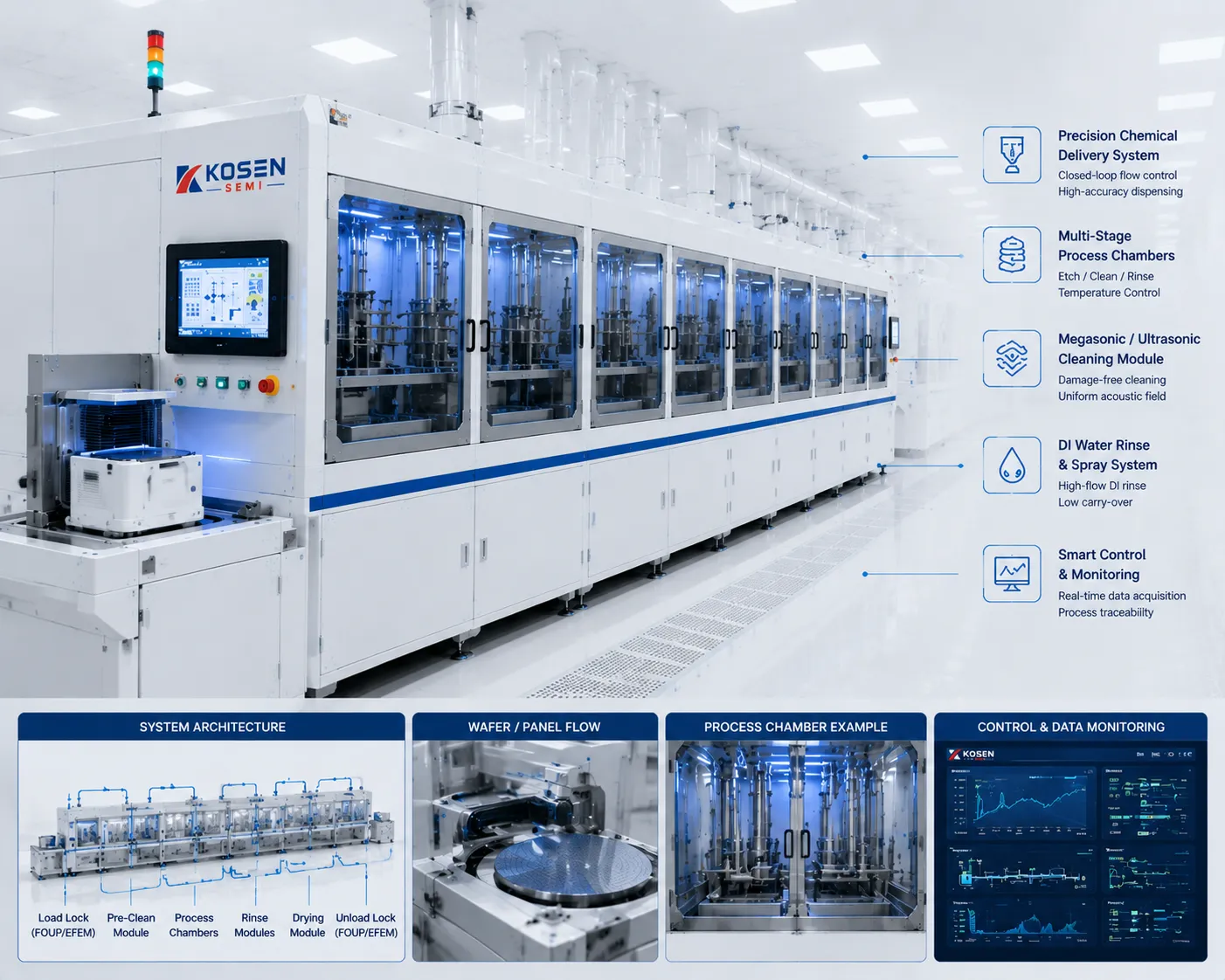
Automated Wet Processing Bench Architecture for High-Volume MEMS Foundries
Overcoming MEMS Fabrication Bottlenecks with Advanced Wet Processing
KOSEN SEMI engineers specialized MEMS wet processing equipment that resolves capillary collapse, acoustic damage, and etch rate drift across high-density semiconductor manufacturing lines. Learn more about us and our history of innovation.
Bulk Micromachining & Anisotropic Etching
Precision silicon cavity shaping in bulk micromachining requires strict crystallographic plane selectivity and dynamic bath control. KOSEN SEMI platforms feature real-time concentration management and inline chemistry dosing for KOH etch control and TMAH processes, maintaining uniform depth control and smooth crystallographic sidewalls across full production runs.
- ✓ Inline Concentration Monitoring: Near-infrared (NIR) sensors continuously track etchant ratios to maintain anisotropic etching rates within ±1.0%.
- ✓ Micro-Roughness Prevention: Automated alcohol and surfactant dosing mitigates hillock formation on etched silicon planes.
- ✓ Thermal Homogeneity: Multi-zone heating elements keep chemical bath temperatures stabilized within ±0.1°C for high process repeatability.
Stiction-Free Sacrificial Layer Release
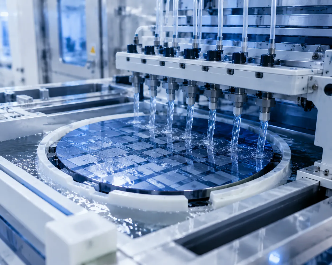
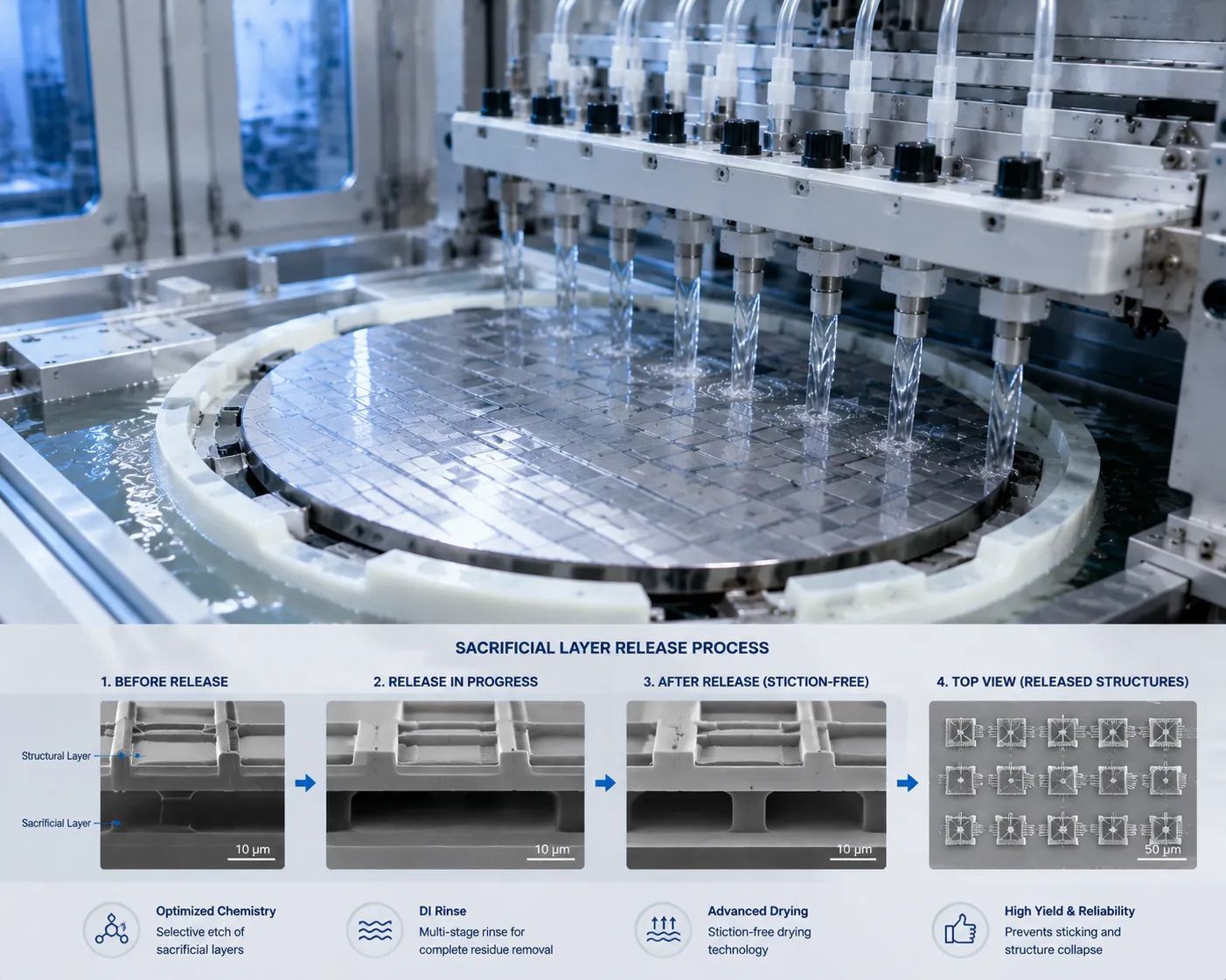
Releasing delicate suspended microstructures demands precise stiction prevention without mechanical collapse. KOSEN SEMI combines low-surface-tension surface conditioning with integrated isopropyl alcohol (IPA) vapor phase drying. Supported by our advanced engineering capability, this neutralizes meniscus forces during liquid displacement, executing damage-free sacrificial layer release for sensitive membranes and micro-cantilevers.
- ✓ Surface Tension Reduction: Tailored chemical rinse sequences eliminate capillary pull during sacrificial oxide removal.
- ✓ IPA Vapor Displacement: Controlled thermal vapor removes liquid instantly, yielding completely dry micro-actuators without beam collapse.
- ✓ Proprietary Recirculation: Closed-loop chemical filtration systems maintain pristine etchant purity throughout high-volume production cycles.
Damage-Free Megasonic Cleaning
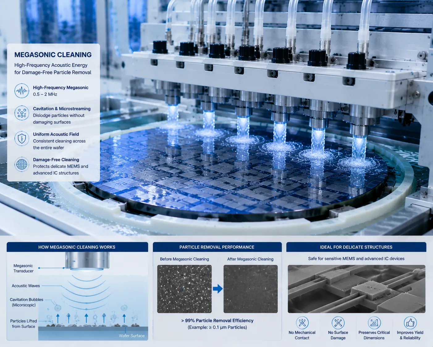
Conventional ultrasonic cleaning introduces violent cavitation that destroys fragile suspended beams. Integrated into our automated wafer cleaning systems, our frequency-modulated megasonic transducer arrays emit uniform acoustic energy from 0.8 MHz to 3.0 MHz. Controlled acoustic streaming delivers 200 nm particle control, with optimized capability down to 100 nm without exerting structural stress on sensitive MEMS devices.
- ✓ Frequency Modulation: Disperses acoustic energy to eliminate destructive standing waves and localized energy hot spots.
- ✓ 200 nm Particle Control, Optimized to 100 nm: Reaches >99% particle removal efficiency for contamination down to 100 nm under optimized conditions.
- ✓ Homogeneous Acoustic Field: Protects high-aspect-ratio RF filters, optical mirrors, and bio-MEMS channel arrays.
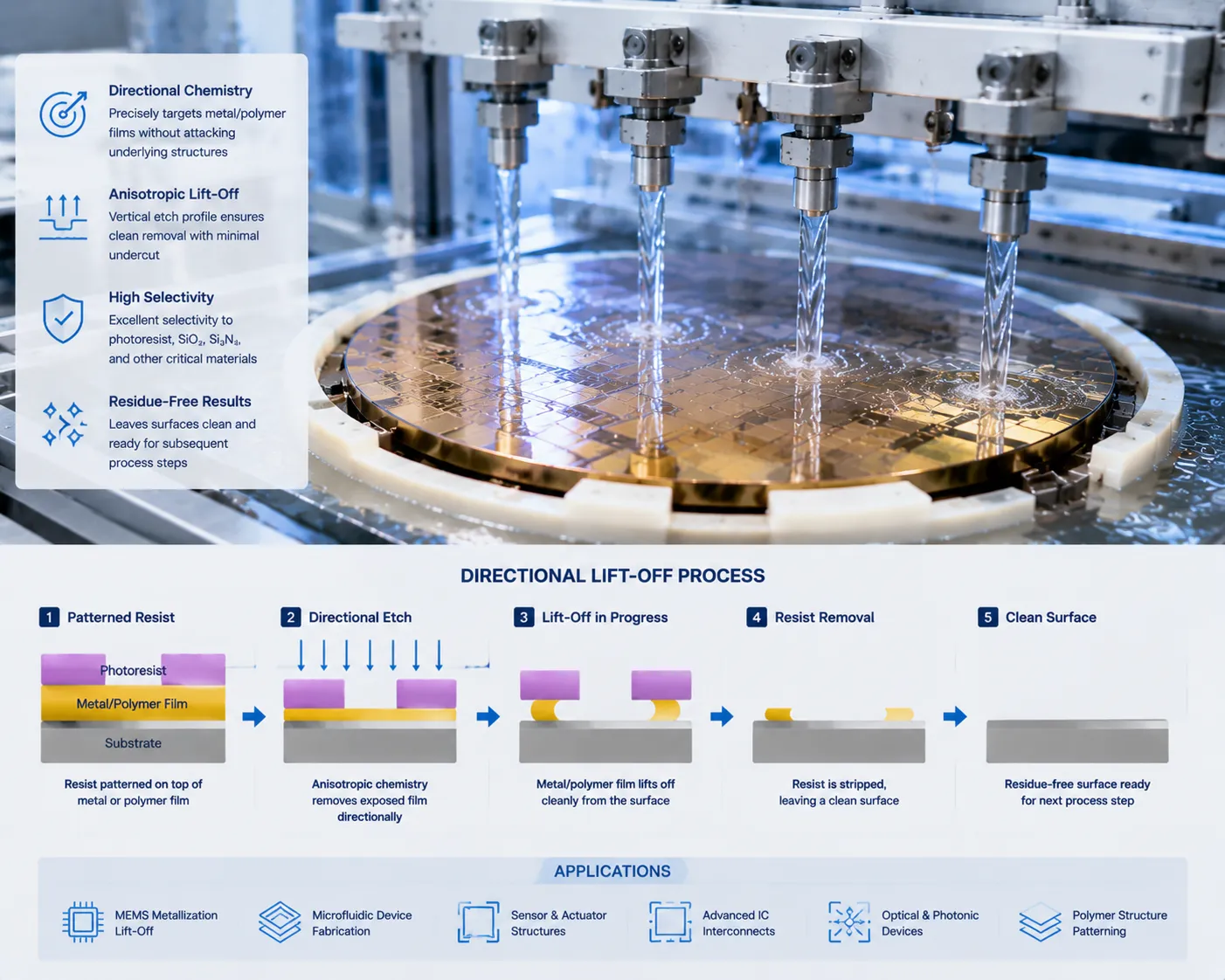
Directional Metal & Polymer Lift-Off
Stripping thick photoresist stacks and deposited metal films often leads to redeposition in narrow micro-cavities. KOSEN SEMI equipment uses high-impact directional solvent spray manifolds paired with continuous point-of-use filtration loops. Solvents dissolve polymers rapidly while inline filtration captures metal flags before re-attaching to fine geometries.
- ✓ Multi-Angle Spray Manifolds: Dynamic nozzle geometry penetrates deep high-aspect-ratio sidewalls cleanly.
- ✓ Active Particulate Capture: Sub-micron filtration loops continuously clean solvent baths during high-volume processing.
- ✓ Explosion-Proof Cabinetry: Fully sealed Ex-proof fluidic containment ensures maximum safety with flammable chemical solvents.
Yield Benchmarking: KOSEN SEMI vs. Conventional Processing
Measurable performance improvements achieved across high-volume MEMS manufacturing lines.
| Process Metric | Conventional Wet Processing | KOSEN SEMI Advanced Platform | Yield Advantage |
|---|---|---|---|
| Sacrificial Layer Release | High capillary stiction rates (>15% beam collapse) | IPA vapor phase displacement (<0.1% defect rate) | +14.9% Yield Improvement |
| 200 nm-Class Cleaning | Structural breakage from standing ultrasonic waves | Frequency-swept megasonic field with zero damage | 99% Removal Efficiency |
| Anisotropic Depth Control | Rate drift (±5.0%) caused by chemical bath depletion | Inline dosing with real-time NIR concentration control | ±1.0% Rate Uniformity |
| Metal Lift-Off Redeposition | Redeposition of metal flags inside micro-cavities | Directional solvent manifolds with continuous filtration | Zero Flag Redeposition |
Ready to Eliminate Yield Bottlenecks in Your Fab?
Our technical team provides custom process recipe testing, fluidic modeling, and equipment configurations tailored to your substrate requirements.
Precision MEMS Wet Etching and Cleaning Systems
Selecting the right hardware architecture is critical for yield optimization and chemical efficiency. KOSEN SEMI designs modular single wafer wet processing tools and high-capacity batch tank benches tailored for MEMS device manufacturing, expanding our innovative products lineup for high-volume fabs.
Single Wafer Wet Processing Systems
Engineered for high-value MEMS devices, our single wafer-cleaning-systems feature isolated multi-chemical dispensing arms and dynamic spin speed control to achieve uniform etch depth and damage-free drying.
Isolated chemical dispensing arms eliminate cross-contamination during multi-step etching and stripping.
Programmable rotation profiles maintain a continuous chemical boundary layer across fragile microstructures.
100% PFA and PTFE fluid paths guarantee ultra-pure chemistry and maximum tool operating longevity.
Point-of-use dosing control minimizes expensive chemical consumption while ensuring etch repeatability.
Single Wafer System Specifications
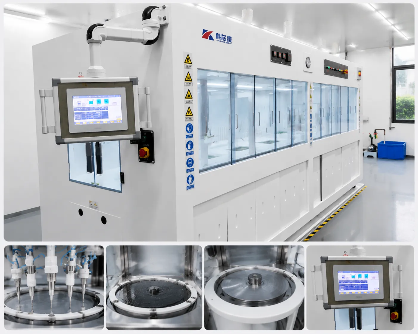
Ideal Application Fit
Optimized for high-value MEMS sensors, optical devices, and sacrificial release steps requiring real-time, wafer-by-wafer process control.
Batch Tank Immersion Benches
Designed for high-volume fab production, our automated batch tank benches combine multi-zone temperature regulation with integrated megasonic cleaning and dynamic recirculation for uniform anisotropic etching.
Frequency-modulated megasonic cleaning arrays remove 200 nm-class particles, with optimized capability down to 100 nm without damaging delicate suspended membranes.
Precision bath temperature management (±0.1°C) ensures highly stable etch rates during KOH and TMAH bulk micromachining.
Continuous chemical filtration extends bath life, lowers chemical usage, and maintains chemical solution purity.
Closed-loop chemical dispensing systems maintain targeted bath concentration throughout extended production runs.
Batch Tank System Specifications
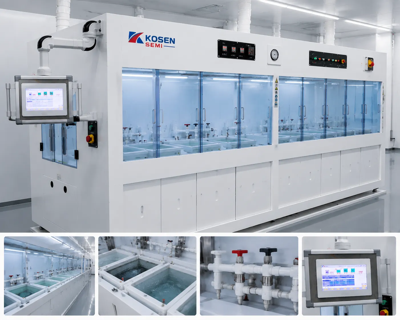
Ideal Application Fit
Engineered for high-volume MEMS pressure sensors, accelerometers, and microfluidics requiring fast turnaround in bulk etching and deep cleaning.
Architecture Specification Matrix
| Hardware Architecture | Single Wafer Systems | Batch Tank Systems |
|---|---|---|
| Process Architecture | Enclosed single substrate process chamber | Automated multi-cassette immersion bench |
| Chemical Dispensing | Multi-chemical spray arms with point-of-use dosing | Automated chemical dispensing & inline recirculation |
| Agitation & Cleaning | Programmable spin speeds & targeted dispensing | Damage-free megasonic cleaning arrays |
| Thermal Control | Point-of-use inline chemical heating | Multi-zone bath temperature control (±0.1°C) |
| Wetted Part Materials | High-Purity Fluoropolymer PFA & PTFE | High-Purity Fluoropolymer PFA & PTFE |
| Primary Strength | High-value single wafer wet processing & precision etch control | High-throughput bulk etching & megasonic cleans |
Need help choosing your hardware architecture?
Our team works closely with global customers to ensure KOSEN SEMI engineers can match tool configurations to your yield and throughput goals.
Rigorous Repeatability and Controlled-Defect Yield Management
In high-volume MEMS manufacturing, subtle bath chemical variations or nanoscale particulate contamination can trigger severe structural collapse and yield destruction. KOSEN SEMI wet processing systems integrate precision fluid dynamics, active thermal isolation, and automated dosing to deliver uncompromised process repeatability and high wafer yields across demanding production runs.
Thermal Control Precision
Precision thermal management maintained within ±0.1°C locks in consistent anisotropic etching rates, preserving crystal plane uniformity and long-term process repeatability.
Particle Control & Cleaning
Advanced inline multi-stage filtration paired with IPA drying suppresses particle add-ons, ensuring strict particle control and thorough 200 nm-class cleaning, optimized to 100 nm in our wafer-cleaning-systems.
Safety & Corrosion Isolation
Explosion-proof design certifications and complete fluidic isolation safeguard operators and machinery during aggressive solvent and acid wet processing.
Full Telemetry Tracking
SECS/GEM interface integration enables real-time telemetry tracking, automated chemical dosing logs, and seamless synchronization with fab MES networks.
Protecting High-Aspect-Ratio Yields in Volume MEMS Fabrication
Uncontrolled chemical degradation, bath aging, or 200 nm-class particulate redeposition during wet etching directly harms delicate suspended beams, membranes, and microchannels. To prevent severe feature undercutting and stiction, KOSEN SEMI builds each platform with active chemical recirculation loops and real-time inline concentration monitoring.
By integrating advanced 200 nm-class cleaning, optimized to 100 nm technologies and megasonic energy controls into Single Wafer Cleaning Systems and batch-tank systems, our platforms remove polymer residues without causing mechanical stress to fragile microstructures. Every component—from high-purity fluidic manifolds to N2-purged tool cabinets—is purpose-built to enforce strict particle control and controlled-defect yield standards.
Verifiable Benchmarks for Fab Audits
- Active Thermal Stability: Multi-zone heating arrays suppress thermal gradients across aggressive KOH and TMAH silicon etching baths.
- High-Purity Contamination Control: Point-of-use PTFE filtration loops maintain controlled particle counts during critical rinsing, release, and surface prep steps.
- Corrosion-Resistant Hardware: Fluoropolymer PFA and PTFE fluid paths guarantee an anti-corrosion operational lifespan exceeding 10 years in high-volume production.
Factory Acceptance Assurance: Every KOSEN SEMI equipment platform undergoes simulated HVM testing before shipment, providing total peace of mind and streamlining on-site fab qualification. Learn more about-us and our commitment to quality.
Process Control Performance
Quantifiable performance benchmarks engineered to surpass standard industry wet bench specifications.
| Parameter | Industry Standard | KOSEN SEMI Baseline |
|---|---|---|
| Etch Temperature Delta | ±0.5°C | ±0.1°C |
| Etch Rate Uniformity | < 3.0% | < 1.5% |
| Particle Add-ons (≥200 nm) | < 15 per wafer | < 3 per wafer |
| Concentration Monitoring | Manual Sampling | Inline Real-Time |
| Wetted Components Life | 5 Years | 10 Years |
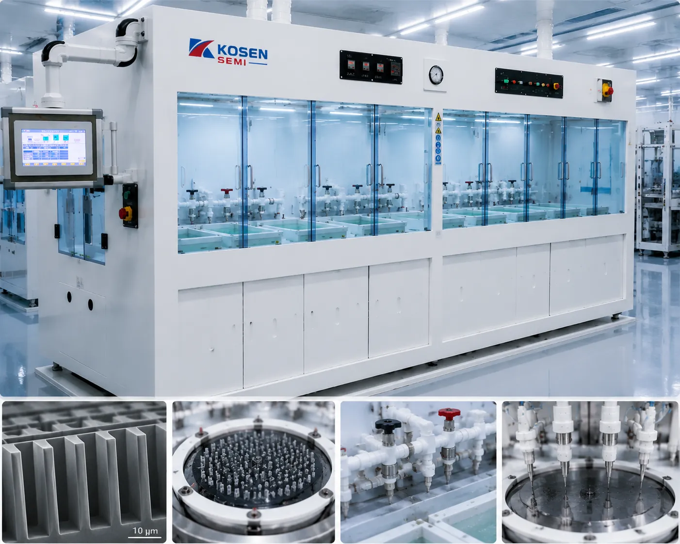
Global Standards & Semiconductor Cleanroom Compliance
Designed and manufactured to meet rigorous international safety, environmental, and automation protocols.
MEMS Wet Processing FAQ
Practical answers to critical technical challenges in MEMS wet processing — covering etch selectivity, stiction prevention, equipment selection, and flexible substrate processing.
Achieving high MEMS etch selectivity and smooth sidewall surface morphology during deep anisotropic silicon etching (such as bulk micromachining for pressure sensors and accelerometers) requires tight multi-variable control across chemical concentration, bath temperature, and active dosing.
- KOH etch control: Maintain KOH concentration within 30–40 wt% using real-time closed-loop chemical monitoring. Keeping concentration tolerances within ±0.2 wt% prevents degradation of the (100)/(111) crystallographic etch ratio and suppresses sidewall micro-roughness.
- Precision thermal management: Regulate bath temperatures to within ±0.1°C to stabilize chemical kinetics. Even minor thermal drift can accelerate lateral etching and disrupt crystallographic plane selectivity across the wafer surface.
- TMAH & surfactant additives: Incorporate specialized additives (such as IPA or custom surfactants) into TMAH or KOH baths to reduce surface tension, prevent silicon hillock formation, and ensure smooth sidewall surfaces on (100) silicon planes.
- Automated chemical replenishment: Closed-loop dosing systems continuously compensate for chemical consumption and evaporation, maintaining consistent chemical bath activity and etch rates across extended multi-wafer production runs.
- Advanced etch-stop mechanisms: Combine heavy boron doping (p+ etch stop) or electrochemical etch stop (ECE) techniques with automated endpoint detection for ultra-precise diaphragm and suspended structure thickness control, backed by KOSEN SEMI's deep Engineering Capability.
KOSEN SEMI platforms integrate real-time concentration monitoring, high-efficiency chemical recirculation, and sub-degree thermal regulation, delivering predictable anisotropic etching performance across high-volume MEMS fabrication lines.