
Semiconductor Wet Processing Core Principles and Applications
Fundamental chemical thermodynamics, surface reaction kinetics, and precision fluid dynamics drive modern semiconductor wet processing across critical wafer fabrication stages.
Synergistic Action of Ultrapure Water and Precision Chemical Liquids
Semiconductor wet processing relies on precisely controlled interactions between specialized liquid chemistries and ultrapure water (UPW) to clean, etch, and condition wafer surfaces. By engineering thermodynamic equilibrium and boundary layer fluid dynamics, automated wet process systems achieve targeted oxidation, trace metal complexation, and electrostatic charge control at the wafer interface. High-purity ultrapure water serves as both an ultra-clean reaction medium and a final rinsing fluid, supporting high-efficiency chemical residue removal and reducing particle re-deposition risk.
Achieving rigorous yield targets at 200 nm standard and 100 nm optimized process conditions requires strict control over bath temperatures, chemical dosing ratios, megasonic energy distribution, and surface wetting mechanisms. Drawing on years of engineering experience, KOSEN SEMI delivers high-precision chemical delivery systems and custom wet processing equipment designed for exceptional bath stability, low chemical consumption, and superior wafer contamination control.
Wet Processing versus Dry Processing Technical Comparison
While dry plasma processing provides high anisotropic vertical etching, semiconductor wet processing remains indispensable for cost-effective batch output, high chemical selectivity, and low-damage wafer surface preparation.
| Parameter | Wet Processing | Dry Processing |
|---|---|---|
| Chemical Selectivity | Ultra-High (>100:1 Ratio) | Moderate to High |
| Throughput Architecture | High-Capacity Batch Output | Sequential Single Wafer |
| Substrate Damage Impact | No Plasma-Induced Lattice Damage | Risk of Plasma-Induced Damage |
| Etch Profile Characteristics | Isotropic Chemical Removal | Anisotropic Vertical Profile |
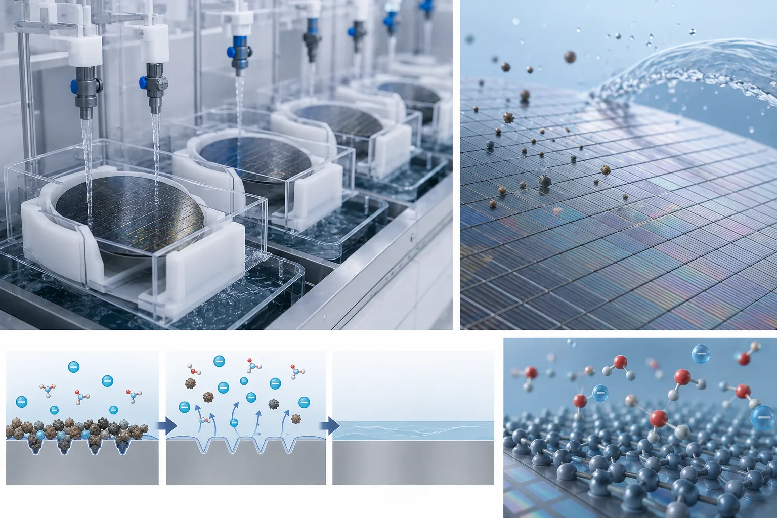
Wafer Cleaning Principles and Surface Kinetics
Effective wafer cleaning principles combine targeted liquid chemistry, zeta-potential charge control, and megasonic acoustic agitation to remove particles at 200 nm under standard conditions and down to 100 nm under optimized conditions without causing structural damage to delicate surface features. Discover our advanced wafer-cleaning-systems to see how these principles are applied in production environments.
Primary Semiconductor Surface Treatment Scenarios
Semiconductor wet process technology underpins critical manufacturing steps across front-end line-of-yield wafer fabrication and back-end advanced packaging.
Surface Cleaning and Contamination Control
Critical wafer surface cleaning targets particles at 200 nm under standard conditions and down to 100 nm under optimized conditions, organic films, and trace metal contamination prior to oxidation, diffusion, and lithography. Standard RCA cleaning steps using ammonium hydroxide, hydrogen peroxide, and hydrochloric acid establish pristine substrates without inducing lattice defects.
- 200 nm Standard / 100 nm Optimized Particle Removal: Zeta-potential repelling forces & megasonics
- Organic Residue Removal: Sulfuric peroxide mixture (SPM) chemical processing
- Native Oxide Etching: Precision dilute hydrofluoric acid (DHF) formulations
Selective Isotropic Etching
Selective wet chemical etching delivers accurate material removal across sacrificial layers, hard masks, dielectric oxides, and thin metal films. Strict bath temperature management and active chemical recirculation ensure uniform etch rates while preserving underlying substrate layers.
- Silicon Nitride Stripping: Hot phosphoric acid wet chemical processing
- Controlled Oxide Etching: Buffered oxide etch (BOE) chemical solutions
- Metal Recess Formation: High-selectivity acid formulations for contact structures
Photoresist Stripping and Polymer Removal
Following dry plasma etching or ion implantation, cross-linked photoresist layers and stubborn sidewall polymers must be completely removed. Formulated solvent chemical baths systematically break down organic matrices without attacking exposed gate dielectrics or sensitive metal lines.
- Bulk Photoresist Removal: Engineered solvent and aqueous bath chemistries
- Post-Etch Residue Cleaning: High-selectivity post-ash polymer removal
- Metallization Protection: Corrosion-inhibited chemistry for copper and aluminum
Core Wet Process Equipment Types and System Architecture
Evaluating equipment architecture is a critical strategic step for fab directors, process engineers, and procurement teams selecting wet etching systems, cleaning systems, and central chemical delivery infrastructure. KOSEN SEMI provides a comprehensive wet processing portfolio—ranging from flexible R&D manual wet benches to high-throughput, fully automated batch systems and advanced single-wafer processing platforms. Below is an architectural breakdown of the three main equipment categories driving modern semiconductor manufacturing.
Automated Wet Bench
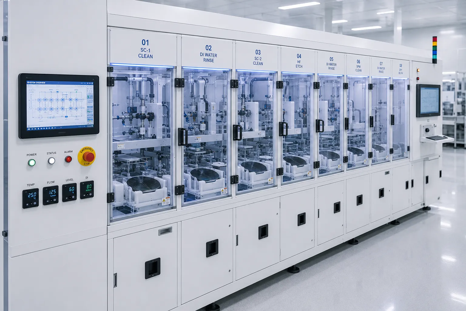
Automated wet benches serve as high-capacity workhorses in modern commercial fabs. Built around a high-throughput architecture tailored for batch processing, these systems clean, etch, and strip multiple wafers simultaneously. This multi-tank sequential approach significantly lowers total Cost of Ownership (CoO) while ensuring repeatable chemical bath controls across high-volume production lines.
Key Technical Parameters
- Batch Capacity: 25–50 wafers per carrier batch (configurable for 150 mm, 200 mm, and 300 mm wafers)
- Chemical Compatibility: Concentrated HF, BOE, Piranha (H2SO4/H2O2), SC-1, SC-2, and custom solvent formulations
- Material Construction: High-purity PTFE, PFA, and Quartz tanks providing superior chemical corrosion resistance
- Automation Level: Fully enclosed multi-axis robotic transfer arms with recipe-driven PLC/PC control
- Throughput Performance: Up to 300+ wafers per hour (WPH) based on active processing steps and recipe sequence
- Cleanroom Compliance: Integrated HEPA/ULPA filtration units maintaining ISO Class 5–7 internal environments
- Process Sequences: Inline RCA cleaning, oxide etching, photoresist stripping, DI water rinsing, and IPA drying
Best For: High-volume manufacturing (HVM) fabs, MEMS, power semiconductors, and compound semiconductor lines prioritizing fast turnaround and lower cost per wafer.
Equipment Architecture at a Glance
Choosing the ideal wet process configuration depends on your wafer size, throughput targets, defectivity limits, and facility requirements. Explore our complete range of wet processing products to evaluate core operational trade-offs across these equipment types.
| Equipment Type | Processing Mode | Primary Strength | Typical Application | CoO Profile |
|---|---|---|---|---|
| Automated Wet Bench | Batch (25–50 wafers) | High throughput, low cost per wafer | Mature nodes, MEMS, power devices | Low — optimized for volume |
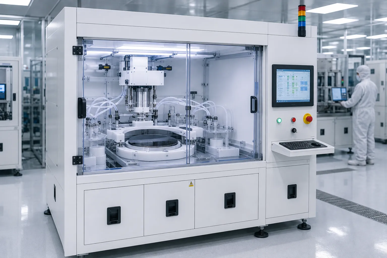
| Single Wafer Cleaning System | Single wafer, spin-spray | High uniformity with minimized cross-contamination risk | Advanced logic, DRAM, 3D NAND | Higher per-wafer, justified by yield gain |
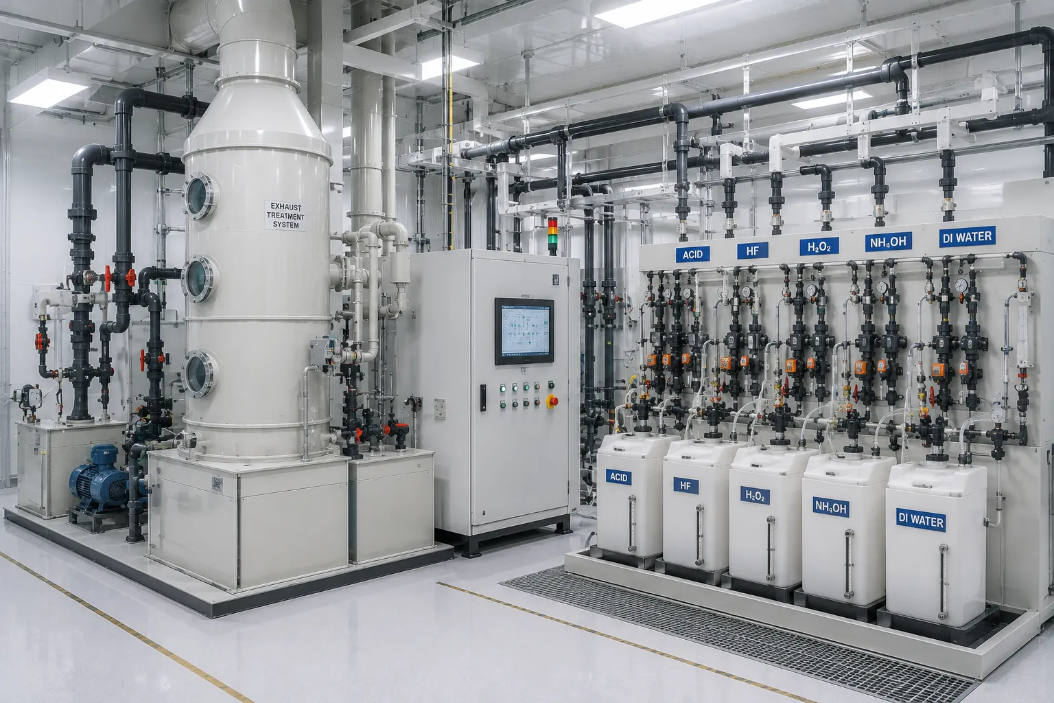
| Scrubber and CDS | Support infrastructure | Safety, compliance, chemical precision | All wet process installations | Mandatory — enables compliant operation |
KOSEN SEMI engineers high-precision wet process equipment spanning manual R&D benches, high-volume automated wet benches, advanced single-wafer tools, and integrated sub-fab chemical delivery solutions. Leveraging our advanced Engineering Capability, our specialists partner directly with your fab team to configure compliant, high-yield processing systems aligned with your unique process recipes and cleanroom footprint requirements.
Wet Process Equipment Selection and Fab Considerations
Selecting high-performance semiconductor surface preparation tools requires balancing chemical compatibility, automation precision, regulatory compliance, and cleanroom footprint. Fabs and process engineers must thoroughly evaluate long-term Cost of Ownership (CoO) alongside strict defectivity limits to ensure maximum yield across 200 nm standard and 100 nm optimized process conditions using advanced wafer cleaning systems.
Chemical Process Compatibility
Selecting inert, high-purity materials supports low metallic contamination levels while withstanding aggressive acids, solvents, and etch chemistries.
- • Virgin PTFE, PFA, PVDF, and fused quartz fluid handling pathways
- • Resistance to concentrated HF, hot H3PO4, SPM, and RCA cleans
- • Closed-loop recirculation with inline filtration and thermal control
Automation Precision & CoO
Advanced robotic handling lowers Cost of Ownership (CoO) through sub-millimeter wafer positioning and reduced chemical drag-out.
- • Multi-axis robotic transfer arms with repeatable positioning accuracy
- • Minimized chemical drag-out and bath life extension capabilities
- • High Overall Equipment Effectiveness (OEE) with automated recipes
Safety & Environmental Compliance
Comprehensive safety integration safeguards fab technicians, facility infrastructure, and process lines from chemical exposure.
- • FM 4910 fire-retardant materials for cabinet construction
- • Cabinet exhaust monitoring, optical flame, and leak detection
- • Segregated chemical drain lines and automated shut-off interlocks
Cleanroom Footprint & Cleanliness
Optimized equipment geometry maximizes cleanroom floor space while maintaining strict mini-environment particle controls.
- • Compact modular design for efficient cleanroom bay integration
- • Integrated ISO Class 5–7 mini-environments with HEPA/ULPA filtration
- • Laminar airflow controls that prevent airborne particle re-deposition
Engineering Evaluation Matrix for Fab Integration
When reviewing wet bench specifications, process engineers must balance tool architecture against target throughput, wafer size, and yield goals. The decision matrix below outlines key trade-offs between high-capacity automated batch wet benches and high-precision Single Wafer Cleaning Systems.
| Evaluation Metric | Automated Batch Wet Bench | Single Wafer Processing Tool |
|---|---|---|
| Wafer Throughput & Output | High volume output (25 to 50 wafers per carrier batch) | Sequential processing tailored for flexible batching |
| Process Uniformity & Yield | Excellent batch-to-batch repeatability for high-volume cleans | Ultra-precise boundary control for advanced technology nodes |
| Chemical Usage & Recirculation | Lower per-wafer chemical consumption via recirculated baths | Fresh chemical dispense mode with targeted spray delivery |
| Cleanroom Footprint Efficiency | Maximum wafer output per square foot of cleanroom floor space | Modular multi-chamber layout adaptable to multi-step flows |
The engineering team at KOSEN SEMI provides customized modular wet bench configuration solutions based on your cleanroom space, chemical dispense needs, and process requirements.
Wet Processing Frequently Asked Questions
Explore technical insights on semiconductor wafer surface preparation, chemical etching, batch wet benches, single-wafer cleaning systems, and fab safety protocols. Our engineering team provides detailed responses to high-frequency queries from fab managers, process engineers, and equipment procurement professionals. Learn more about-us and how we serve global users.
Semiconductor manufacturing relies on both wet processing and dry processing to achieve critical wafer surface modifications, but their underlying chemical and physical mechanisms differ fundamentally. Wafer wet processing uses liquid chemical solutions, ultrapure water (UPW), and specialized surfactants to perform isotropic etching, 200 nm standard particle removal with optimized capability down to 100 nm, and post-etch residue stripping in high-performance wafer-cleaning-systems.
In contrast, dry processing utilizes energetic plasma, reactive gas species, or ion beams to perform anisotropic etching and thin-film deposition in high-vacuum chambers. While dry etching excels at generating ultra-fine vertical features for high-aspect-ratio patterns, wet processing remains essential for high-throughput surface preparation, metal contaminant removal, wafer conditioning, and chemical oxide strip operations due to its exceptional chemical selectivity and lower cost per wafer.
- Chemical Mechanism: Liquid chemical baths versus plasma reactive ion etching (RIE)
- Selectivity: High isotropic chemical selectivity in wet chemistry versus directional physical impact in plasma
- Primary Role: Comprehensive surface preparation, particle control, and photoresist residue removal
Choosing the right equipment configuration depends heavily on production volume, process window requirements, technology node, and cost of ownership targets. Automated batch wet benches process 25 to 50 wafers simultaneously per chemical tank, delivering high throughput (up to 300 wafers per hour) and minimal chemical consumption per wafer. They are ideal for high-volume manufacturing, legacy nodes, MEMS, power devices, and general wafer cleaning lines.
Advanced Single Wafer Cleaning Systems process one wafer at a time using high-speed rotation, targeted chemical dispenses, and megasonic nozzle agitation. Single-wafer processing minimizes cross-contamination risks, provides precise edge-exclusion control, and delivers superior film uniformity needed for 200 nm standard and 100 nm optimized logic and memory processes.
| Evaluation Metric | Automated Batch Wet Bench | Single-Wafer Processing System |
|---|---|---|
| Throughput Capability | High capacity (150 to 300 WPH) | Moderate capacity (30 to 60 WPH per chamber) |
| Chemical Consumption | Low per wafer via recirculated baths | Higher per wafer via fresh chemical dispense |
| Defectivity Control | Excellent for micro-particles | Low defectivity with minimized cross-contamination risk |
| Target Technology Node | 200 nm standard processes, Power, MEMS | 100 nm optimized processes, 3D NAND, DRAM |
Maintaining wet processing equipment involves working with highly corrosive acids, strong bases, organic solvents, and elevated chemical bath temperatures. Equipment safety and cleanroom protection demand strict engineering safeguards and operational protocols.
Key safety guidelines include continuous exhaust pressure monitoring to prevent toxic vapor accumulation, automated chemical leak sensors with secondary containment sumps, Emergency Off (EMO) integration, and Factory Mutual FM 4910 compliance for fire-retardant fluoropolymer materials such as PTFE, PFA, and PVDF.
- Material Selection: High-purity fluoropolymer construction to eliminate corrosion and ion leaching
- Line Purging: Automated high-purity nitrogen purge routines prior to chemical valve servicing
- Personal Protection: Full acid-resistant personal protective equipment (PPE) and mandatory dual-technician verification
Micro-contamination is the leading cause of yield loss in wafer surface treatment. Chemical Delivery Systems (CDS) must maintain ultra-high purity levels from bulk chemical supply units all the way to point-of-use dispense nozzles.
Integrating continuous inline particle filtration at 200 nm under standard conditions and down to 100 nm under optimized conditions, utilizing megasonic fluid agitation, and deploying isopropyl alcohol (IPA) Marangoni drying systems ensures wafer drying without water mark defects or metallic residue contamination.
Our after-sales service team not only provides equipment installation but also offers complete wet process training and year-round technical support for customers. We partner closely with semiconductor manufacturers to ensure optimal tool uptime, process repeatability, and compliance with strict cleanroom operational standards.
From initial cleanroom footprint planning and modular wet bench customization to process recipe development and preventative maintenance contracts, KOSEN SEMI offers comprehensive lifecycle management for your wafer surface processing infrastructure.
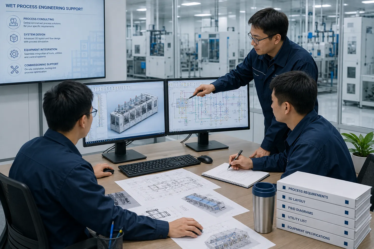
Integrated Wet Process Engineering Support
KOSEN SEMI delivers high-purity automated wet benches, single-wafer cleaning systems, and chemical delivery units tailored to your fab requirements.
Need assistance selecting between batch and single-wafer systems? Speak with a KOSEN SEMI application specialist today.
Ready to Plan Your Next Wet Process Project?
Connect with KOSEN SEMI application specialists for a free technical evaluation. Backed by our advanced Engineering Capability, we specialize in high-performance semiconductor wet bench systems and single wafer cleaning systems to help you build high-yield, compliant, and scalable wafer processing lines.
Engineering inquiries typically reviewed within 24 hours.