
Quantifiable Micro-Level Cleanliness for Compound Semiconductors
KOSEN SEMI delivers precision wet processing systems engineered to advance SiC process control and maximize GaN substrate yield across high-volume fabs.
Metal Contamination Removal
Wafer surface metal impurity elimination down to sub-ppb levels, validated via ICP-MS analysis.
Etching Uniformity Control
Tight process window precision optimized for ultra-thin SiC and GaN epitaxial films.
Chemical Delivery Downtime
Continuous, corrosion-resistant chemical delivery architecture ensuring stable, uninterrupted fab operations.
Fab Deployments
Proven mass production line implementations in commercial SiC and GaN manufacturing facilities.
Precision Chemical Processing Engineered for SiC & GaN Manufacturing
Compound semiconductor manufacturing demands micro-level cleanliness and uncompromising chemical control. KOSEN SEMI supplies scalable wet processing equipment, including advanced Single Wafer Cleaning Systems, engineered to enhance SiC process control and optimize GaN substrate yield without compromising sensitive substrate topographies.
ICP-MS Trace Validation
Analytical chemical verification for our semiconductor-wet-bench-systems guarantees compliance with sub-ppb cleanliness and particle control targets.
Corrosion Resistance
High-purity fluoropolymer fluid pathways maintain total reagent integrity in aggressive acid and solvent processes.
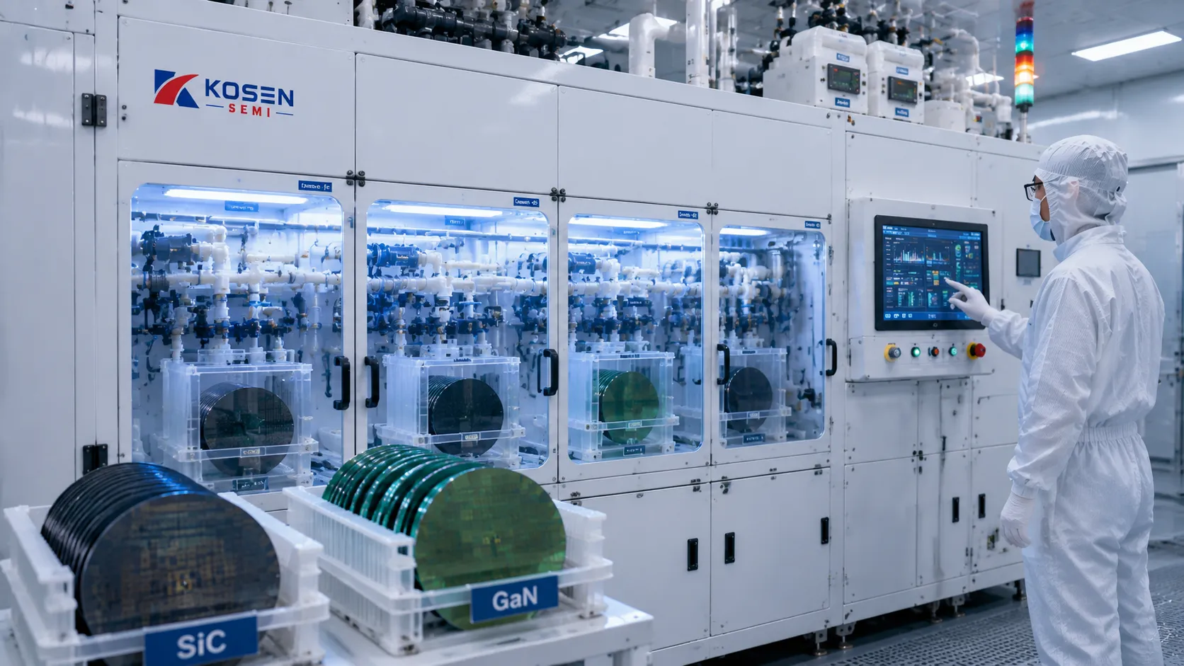
Enhance GaN Substrate Yield & SiC Process Control
Consult with KOSEN SEMI process specialists to deploy certified wet cleaning and etching solutions in your fab.
Tailored Wet Processing Across Compound Substrate Chemistries
Compound semiconductor substrates—ranging from wide-bandgap Silicon Carbide and Gallium Nitride to fragile III-V materials—present unique lattice structures, chemical inertness, and thermal boundaries that standard silicon wet processing tools cannot accommodate. KOSEN SEMI delivers dedicated compound semiconductor equipment and automated wet processing platforms engineered specifically for advanced SiC, GaN, and III-V wafer manufacturing.
By integrating multi-frequency megasonic wafer cleaning equipment, sustained high-temperature chemical loops, and custom fluid dynamics, our single wafer processing and batch platforms prevent lattice damage, control 200 nm-class defectivity, with optimized capability down to 100 nm, and deliver quantifiable yield optimization across power, RF, and optoelectronic device fabrication lines.
Silicon Carbide (SiC) Wafer Processing Solutions
Silicon Carbide substrates exhibit extreme mechanical hardness and chemical inertness, requiring aggressive chemistries at elevated temperatures combined with high-impact physical agitation to achieve 200 nm-class cleanliness, with optimized capability down to 100 nm after wire sawing, grinding, and CMP. KOSEN SEMI platforms incorporate full fluoropolymer fluidics and sustained high-temperature thermal loops engineered specifically for rigorous SiC process control in 150mm and 200mm production lines.
Core Capability Highlights
- ✓
Sliced Wafer Post-Grinding Cleaning: Removes sub-surface damage particles, wire-saw slurry residue, and heavy oils through multi-frequency megasonic bath agitation and targeted acoustic action.
- ✓
Substrate Thinning Residue Removal: Employs recirculating high-temperature SPM and SPRM chemical baths up to 180°C to dissolve tough organic contaminants without pitting the underlying SiC crystal lattice.
- ✓
High-Hardness Surface Passivation: Prepares inert 4H-SiC and 6H-SiC wafer surfaces for homoepitaxial growth with surface micro-roughness strictly controlled under 0.1 nm RMS standards.
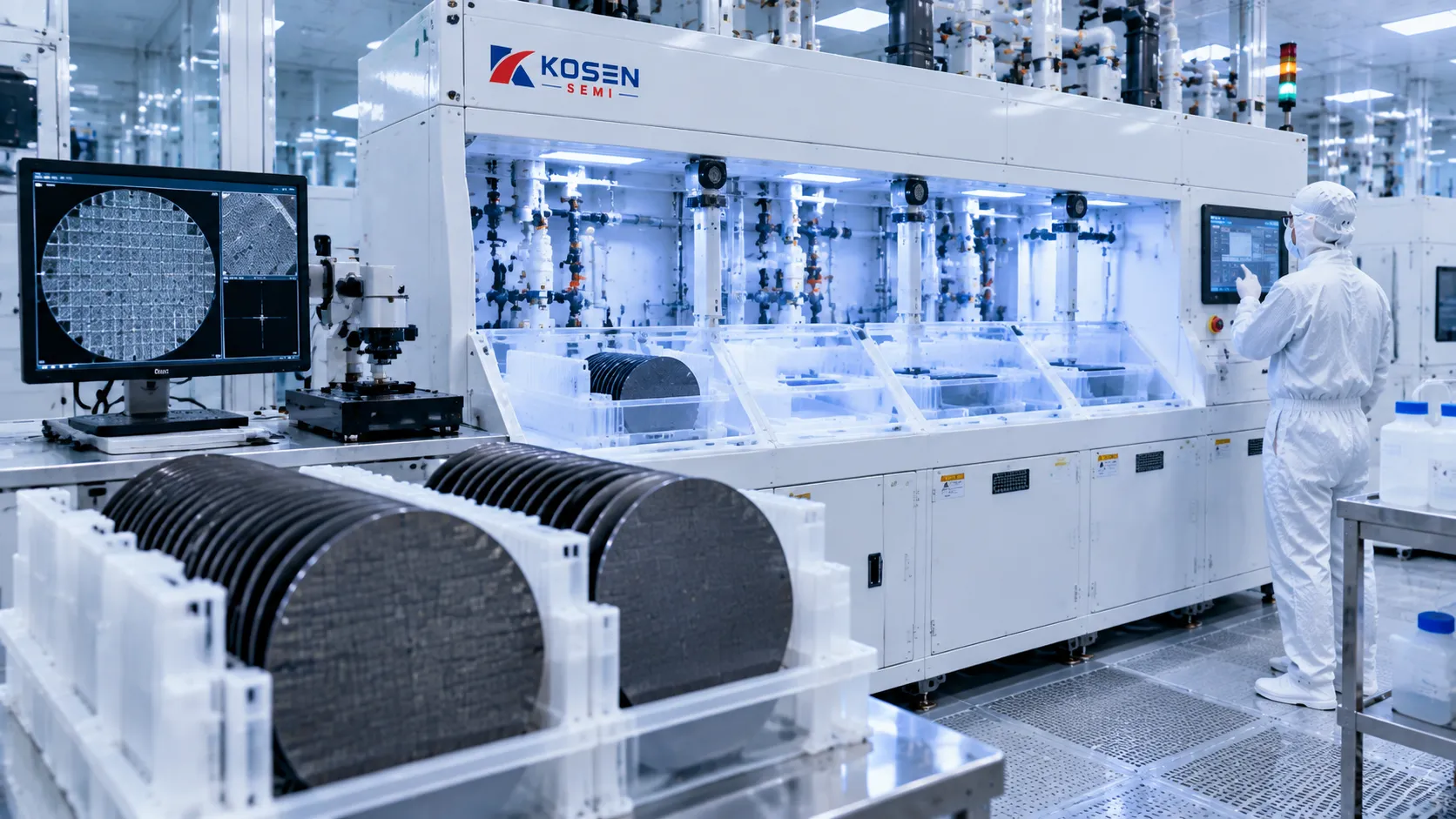
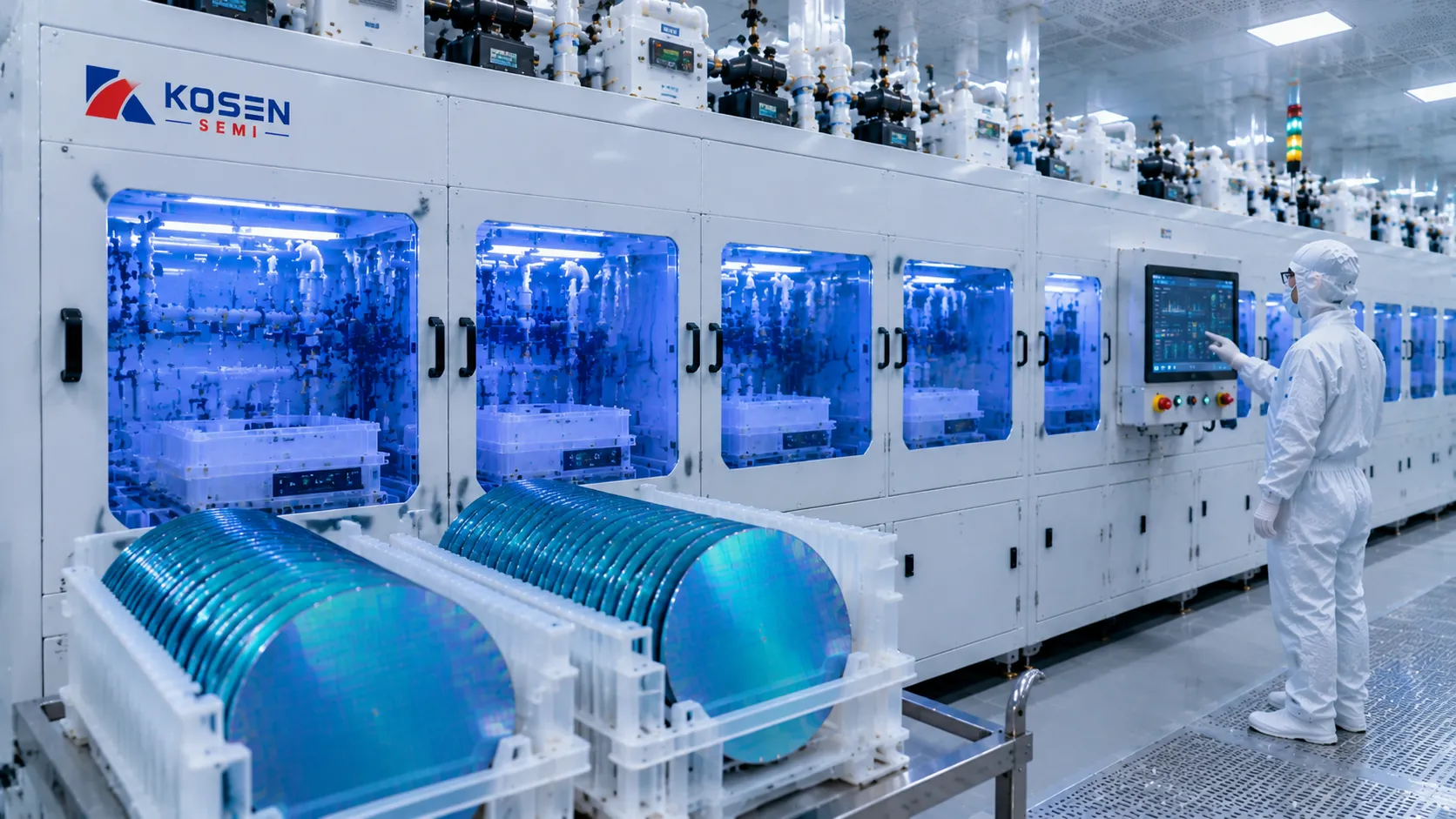
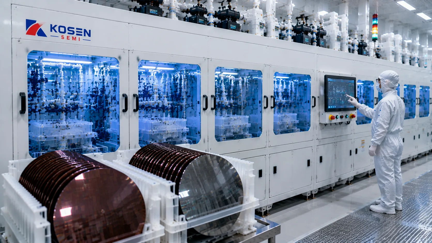
Thermal Management and Custom Fluid Dynamics Engineering
Substrate Physics and Chemical Dynamics
Mastering specialized chemistries in SiC and GaN manufacturing demands custom hardware engineering that addresses differing crystal lattice constants and thermal expansion boundaries. Standard silicon wafer processing relies on ambient or low-temperature chemical baths. In contrast, Silicon Carbide processing requires aggressive chemical mixtures operating near boiling thresholds. KOSEN SEMI platforms incorporate dual-walled PTFE heating tanks with inline infrared temperature monitoring to maintain bath stability up to 180°C.
Conversely, fragile III-V compound semiconductor materials like GaAs and InP exhibit extreme chemical vulnerability and mechanical brittleness. Uncontrolled fluid turbulence or rapid temperature shifts can induce micro-cracking or layer delamination. Our automated chemical delivery systems balance thermal ramps with precise fluid velocity profiling to eliminate thermal shock risks during critical chemical transitions.
Optimized Flow Control Across Substrate Chemistries
Fluid recirculation and particle filtration dynamics are explicitly configured for each substrate family. In GaN epitaxial wafer processing, organic metal-organic chemical vapor deposition (MOCVD) byproducts require high-turnover chemical recirculation loops with sub-0.05 μm fluoropolymer filter membranes. This prevents particle re-deposition during extended immersion and spray cleaning cycles.
By combining real-time chemical concentration analysis with automated dosing units, KOSEN SEMI platforms ensure consistent chemical activity across thousands of processing cycles. This multi-material versatility grants semiconductor fabs dependable process repeatability tailored directly to their compound wafer roadmap.
| Process Parameter | Silicon Carbide (SiC) | Gallium Nitride (GaN) | GaAs and InP Compounds |
|---|---|---|---|
| Primary Chemical Environment | High-Temp SPM, SPRM, Concentrated HF | Selective Acid/Base Strippers, SC-1, SC-2 | Solvent Lift-Off Chemistries, Dilute Mineral Acids |
| Operating Temperature Window | Up to 180°C Continuous | 40°C to 90°C Regulated | Ambient to 65°C Precise |
| Fluid Mechanics Profile | High-Impact Cavitation Megasonics | Controlled Boundary-Layer Laminar Flow | Low-Shear Soft Spray & Marangoni Vapor |
| Defectivity & Cleanliness Target | Particle & Organic Removal down to 100 nm under optimized conditions | Sub-ppm Metal Removal (ICP-MS Validated) | Controlled Metal Residue & Feature Protection |
Require Customized Chemical Bath Configurations for Your Substrate?
KOSEN SEMI process engineers evaluate your specific wafer crystal parameters, slurry chemistry, and throughput requirements to build custom compound semiconductor solutions.
Automated Architecture & Chemical Delivery Systems
Engineered specifically for harsh compound semiconductor wet processing, combining fully sealed fluoropolymer containment with high-precision chemical delivery and single wafer cleaning systems capabilities.
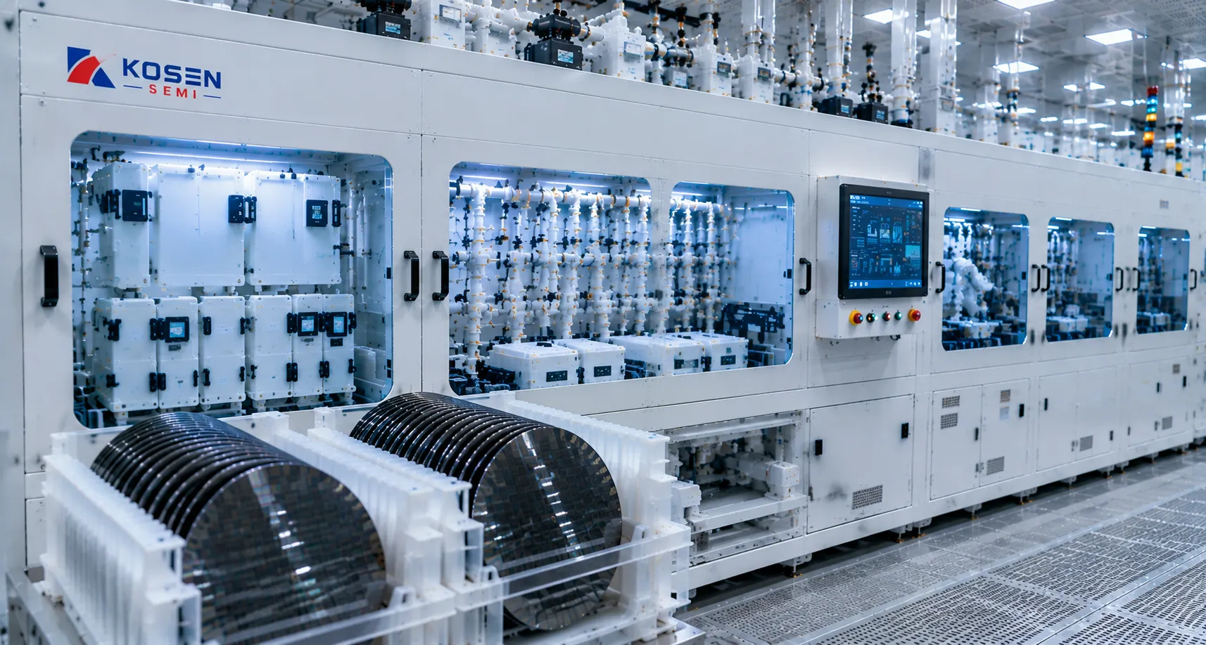
PFA / PTFE Linings Spec 01
Fully sealed fluoropolymer cabinets block corrosive chemical vapors completely.
Chemical Delivery System Spec 02
In-line concentration sensors drive automated auto-dosing to maintain bath chemistry.
Single Wafer & SECS/GEM Robotics Spec 03
Precision robotic handling ensures reproducible single wafer processing across fab runs.
Anti-Corrosive Fluoropolymer Hardware
Fully enclosed PFA and PTFE linings isolate aggressive high-temperature chemistry, maximizing equipment life in demanding SiC/GaN fab manufacturing environments.
Automated Chemical Delivery System
Real-time inline concentration analysis triggers precise chemical re-dosing, preventing bath drift and ensuring etch rate consistency.
Single Wafer Processing & SECS/GEM
Automated robotic transport delivers gentle, repeatable single wafer processing while interfacing seamlessly with host SECS/GEM MES.
Architecture Technical Specifications
| System Module | Material & Design Spec | Automation Protocol | Compound Semi Advantage |
|---|---|---|---|
| Cabinet Enclosure | PFA and PTFE fluoropolymer linings | Sealed anti-leak vapor containment | Protects fab equipment from hot acid vapors |
| Chemical Delivery System | High-purity fluoropolymer manifolds & sensors | Closed-loop real-time concentration analysis | Eliminates process bath chemical drift |
| Single Wafer Transport | ISO Class 5–7 cleanroom compatible robotic arm | SECS/GEM factory integration standard | Ensures high-throughput, operator-free processing |
| Safety & Fluid Control | Dual-contained chemical supply line network | Automated emergency shutdown & line purging | Prevents chemical leaks and contamination |
Upgrade Your Cleanroom Chemical Delivery Architecture
Consult with KOSEN SEMI engineers to customize PFA/PTFE chemical delivery systems and integrated wafer cleaning systems tailored to your fab requirements.
Precision Wet Etching & Cleaning Systems for Compound Wafer Processing
High-yield chemical surface preparation engineered specifically for SiC, GaN, GaAs, and InP microelectronics, optical devices, and high-power RF applications.
Wafer Metal Removal Rate
Trace surface metallic contamination eliminated and validated via ICP-MS analysis protocols.
Etch Uniformity Precision
Tight boundary layer control supporting ultra-thin SiC, GaN, and III-V active films.
Unplanned Chemical Downtime
Continuous continuous-duty delivery in high-purity hot acid and aggressive solvent environments.
Fab Line Deployments
Production-proven automated tools running in active 150mm and 200mm global foundries.
Frequently Asked Questions
Addressing key technical and operational questions regarding KOSEN SEMI compound wafer wet processing equipment.
Consult KOSEN SEMI Engineers for Custom Wet Processing Solutions
Share your SiC, GaN, GaAs, or InP wafer requirements with our engineering team. We provide customized recommendations for cleaning, etching, chemical compatibility, and equipment configuration.
Frequently Asked Questions
Overcoming Compound Substrate Processing Challenges
Manufacturing wide-bandgap compound semiconductors like SiC, GaN, and III-V substrates presents extreme wet processing challenges. High thermal thresholds, aggressive acid chemistries, and stringent defect density limits demand highly specialized equipment architectures. KOSEN SEMI delivers field-proven wet bench and Single Wafer Cleaning Systems engineered to withstand harsh chemical environments, optimize yield, and resolve critical production bottlenecks.
Does the platform support both single-wafer processing and batch wet bench configurations?
Yes. KOSEN SEMI manufactures both single-wafer processing modules and automated full-batch wet benches tailored for compound semiconductor manufacturing. Single-wafer platforms excel at ultra-precise surface cleaning, high-selectivity thin-film etching, and delicate pattern protection where cross-contamination must be strictly eliminated. Automated batch wet benches deliver maximum wafer throughput for high-volume substrate production, post-grinding damage removal, and bulk strip operations.
- Single-wafer precision: Dedicated fluid control for sensitive epitaxy layers, ultra-thin films, and fine-pitch device architectures.
- High-throughput batch benches: Optimized carrier kinematics and multi-tank sequencing engineered for high-volume fab lines.
- Modular integration: Shared chemical delivery infrastructure, controls, and safety frameworks across both tool styles.
How are tool longevity and maintenance managed in high-temperature acid environments?
KOSEN SEMI wet processing tools utilize high-purity fluoropolymers (PTFE/PFA) across all chemical wetted pathways and processing tanks. Continuous nitrogen gas-purge sealing creates positive-pressure barriers around electrical actuators, mechanical joints, and structural enclosures. This robust architecture resists aggressive sulfuric acid and hydrogen peroxide (SPM/SPRM) mixtures running at temperatures up to 180°C, extending component lifespan and lowering cost of ownership.
- 300% longer life: High-grade fluoropolymer construction prevents chemical oxidation, stress cracking, and material degradation.
- N2 gas-purge isolation: Positive-pressure vapor barriers seal driving mechanisms away from corrosive acid fumes.
- Thermal stability: Advanced bath heating and circulation prevent thermal shock and maintain uniform temperature gradients.
Can fluid delivery systems and manifolds be customized for proprietary chemistry blends?
Absolutely. KOSEN SEMI process engineers custom-design chemical delivery manifolds, auto-dosing units, and drainage plumbing tailored precisely to your fab's proprietary chemical formulations and safety protocols. Integrated closed-loop chemical reclaim systems achieve dynamic recovery rates exceeding 90 percent, significantly reducing raw material consumption and hazardous waste treatment costs.
- Real-time auto-dosing: Online concentration sensors trigger precise replenishment to preserve bath chemical equilibrium.
- Closed-loop reclaim: Dynamic chemical recycling (>90% recovery) minimizes chemical expense and waste handling.
- Segregated plumbing: Dedicated drain separation prevents unintended chemical mixing and maintains strict safety standards.
Are KOSEN SEMI wet processing tools certified for ISO Class 5–7 cleanrooms and SECS/GEM automation?
Yes. All KOSEN SEMI compound semiconductor wet processing platforms meet ISO Class 5–7 cleanroom standards. Systems come standard with fully compliant SECS/GEM communication protocols, enabling seamless integration with Manufacturing Execution Systems (MES) for automated recipe downloading, data logging, and real-time process monitoring. Fully automated robotic wafer handling eliminates operator contamination and micro-fracture risks.
- ISO Class 5–7 compliance: High-efficiency particle filtration and enclosed laminar flow maintain ultra-clean operation.
- Native SECS/GEM integration: Full software compliance supports automated recipe management and MES tracking.
- Precision robotic transfer: Gentle end-effector kinematics prevent mechanical stress and edge chipping on SiC/GaN wafers.
How do these wet processing platforms optimize yield and eliminate defects on SiC and GaN substrates?
Compound substrate fabrication demands 200 nm-class particle removal, with optimized capability down to 100 nm and rigorous metallic contamination control. KOSEN SEMI platforms incorporate multi-frequency megasonic transducers and watermark-free IPA Marangoni drying. Rigorous testing validates a 99.8 percent metal contamination removal rate and tight etch uniformity within ±1.5 percent across wide-bandgap wafer surfaces.
- 200 nm-Class Particle Removal: Advanced megasonic agitation dislodges particles down to 100 nm under optimized conditions without damaging delicate features.
- IPA Marangoni drying: Surface-tension-driven drying eliminates watermarks and residue stains on sensitive micro-patterns.
- High etch uniformity: Closed-loop chemical thermal control yields precise thin-film etching tolerances within ±1.5%.
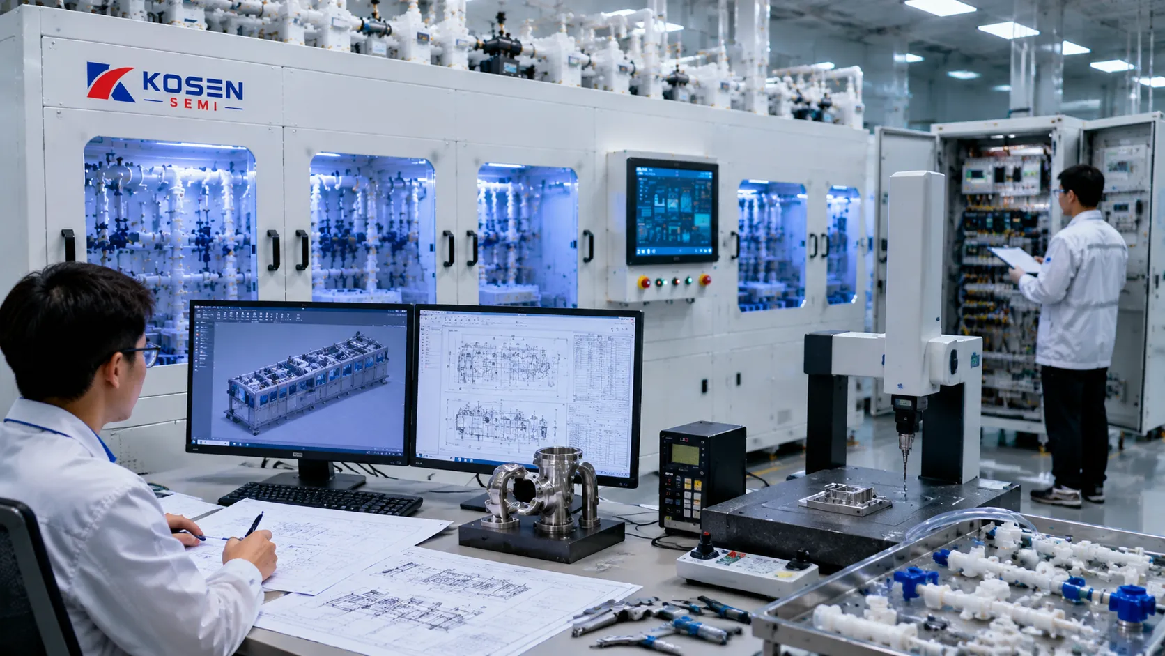
Engineering Specifications and Standards
KOSEN SEMI wet processing systems for compound semiconductor fabs are certified to meet rigorous global semiconductor standards.
| Parameter | Specification |
|---|---|
| Cleanroom Rating | ISO Class 5–7 |
| Max Acid Temp | Up to 180°C (SPM/SPRM) |
| Chemical Reclaim | 90% dynamic recovery |
| Automation | Full SECS and GEM interface |
| Particle Limit | 100 nm under optimized conditions particle control |
Direct Engineer Consultation
Need detailed chemical compatibility matrixes or custom tool footprint layouts? Our process team provides tailored technical evaluations within 24 hours.
Over 100 KOSEN SEMI compound semiconductor wet processing modules are actively deployed in high-volume manufacturing fabs worldwide.
Ready to Maximize Your Compound Wafer Yield and Process Stability?
Submit your substrate parameters (SiC, GaN, III-V) and target specifications. Our engineering team will evaluate your clean, etch, or strip requirements using our advanced Single Wafer Cleaning Systems to deliver a customized wet processing evaluation report within 24 hours.
24-Hour Evaluation
Receive comprehensive technical reports with chemical recipe and throughput recommendations.
Tailored Solutions
Fully optimized custom compound semiconductor solutions for SiC, GaN, GaAs, and InP fabbing.
Trust Commitment
100% Data Confidentiality Guaranteed. Strict NDA Compliance & IP Security.
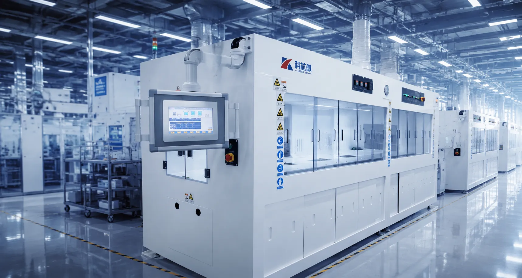
Consult a Process Engineer
Connect with our team to learn more about our Engineering Capability and design custom compound semiconductor solutions tailored to your fab requirements.