
Specialized SiC Wafer Cleaning & GaN Surface Preparation
Third-generation power devices based on Silicon Carbide (SiC) and Gallium Nitride (GaN) are driving unprecedented energy efficiency in electric vehicles, industrial power systems, and renewable grids. However, extreme physical hardness, high chemical inertness, and ultra-sensitive heterojunction architectures present severe wet processing hurdles. KOSEN SEMI delivers high-precision semiconductor wet bench systems engineered to conquer substrate defects, remove persistent post-CMP residues, and support controlled surface cleanliness while minimizing impact on underlying active layers.
SiC Wafer Cleaning: Overcoming Hardness & Chemical Inertness
Silicon Carbide substrate preparation relies on aggressive Chemical Mechanical Planarization (CMP), which leaves 200 nm-class slurry particles, with optimized removal down to 100 nm and embedded organic residues bound to the crystalline lattice. KOSEN SEMI utilizes elevated chemical temperatures and optimized acoustic fluid dynamics to clear micro-contaminants without inducing surface scratches or lattice damage.
- High-Temperature Chemical Formulations: Precision-heated, high-concentration chemical dispense breaks down recalcitrant post-CMP slurry binders and organic impurities.
- Subsurface Defect Mitigation: Controlled fluid shear forces purge micro-voids and surface pits while maintaining exact planar substrate geometry.
- Pre-Epitaxial Surface Preparation: Supports consistent Si-face and C-face surface preparation to reduce contamination-related epitaxial defects.
GaN Surface Preparation: Protecting Sensitive Epitaxial Layers
Gallium Nitride device manufacturing requires precise process control across ultrathin heterojunction layers. Aggressive chemistry risks over-etching active barrier structures, which severely degrades two-dimensional electron gas (2DEG) mobility. Our process controls native oxide removal with repeatable etch control for 200 nm processes, with optimized capability down to 100 nm.
- Hyper-Precise Surface Oxide Stripping: Ultra-dilute, temperature-controlled chemical etching engineered to strip native oxides without attacking AlGaN/GaN barriers.
- Pitting-Free Surface Passivation: Self-limiting chemical reactions neutralize surface states and prevent re-oxidation prior to contact metallization.
- Non-Contact Thin Wafer Handling: Bernoulli-effect handling and gentle liquid cushions protect fragile GaN-on-Si, GaN-on-Sapphire, and GaN-on-QST wafers from mechanical stress.
Compound Semiconductor Process Capability Benchmarks
Quantitative yield and contamination control performance metrics achieved across high-volume 150mm and 200mm compound semiconductor fabs.
| Process Target | SiC Substrate Solution | GaN Epitaxy Solution | KOSEN SEMI Benchmark |
|---|---|---|---|
| Post-CMP Particulate Removal | Heated chemical bath + tailored megasonics | Controlled fluid boundary-layer rinse | Particle count verified per configured process at ≥200 nm, with optimized evaluation down to 100 nm |
| Surface Oxide Control | Subsurface micro-pit chemical clearing | Controlled native oxide stripping | Process-specific etch-rate repeatability |
| Trace Metal Contamination | Multi-acid metallic chelating chemical rinse | Alkali ion residue neutralization | < 1E10 atoms/cm² |
| Substrate Integrity | Reduced step-bunching risk | Heterojunction 2DEG layer preservation | Controlled surface preparation for mobility retention |
Integrated Multi-Stage Wet Chemical Processing Workflow
An engineered sequential chemical flow balancing particulate removal with controlled surface finishing.
Thermal Chemical Agitation
High-temperature, high-concentration chemical formulations dissolve organic binders and dislodge stubborn embedded post-CMP slurry particles.
Precision Oxide Stripping
Hyper-precise surface oxide stripping removes native oxide films while fully protecting sensitive heterojunction active layers.
Megasonic Cavitation Rinsing
Uniform acoustic energy field sweeps away 200 nm-class contaminants, with optimized removal down to 100 nm without inducing crystalline micro-fractures or surface pits.
Marangoni Vapor Drying
Surface-tension-gradient drying helps reduce watermarks and chemical drying spots while supporting consistent substrate surfaces.
Engineered for Compound Semiconductor Production
KOSEN SEMI provides compound semiconductor manufacturers with flexible equipment platforms suitable for both pilot R&D lines and high-volume 24/7 manufacturing environments. Whether deploying single-wafer tools for high-value SiC epi-cleans or batch cleaning systems for high-throughput substrate production, our equipment supports yield stability and efficient total cost of ownership.
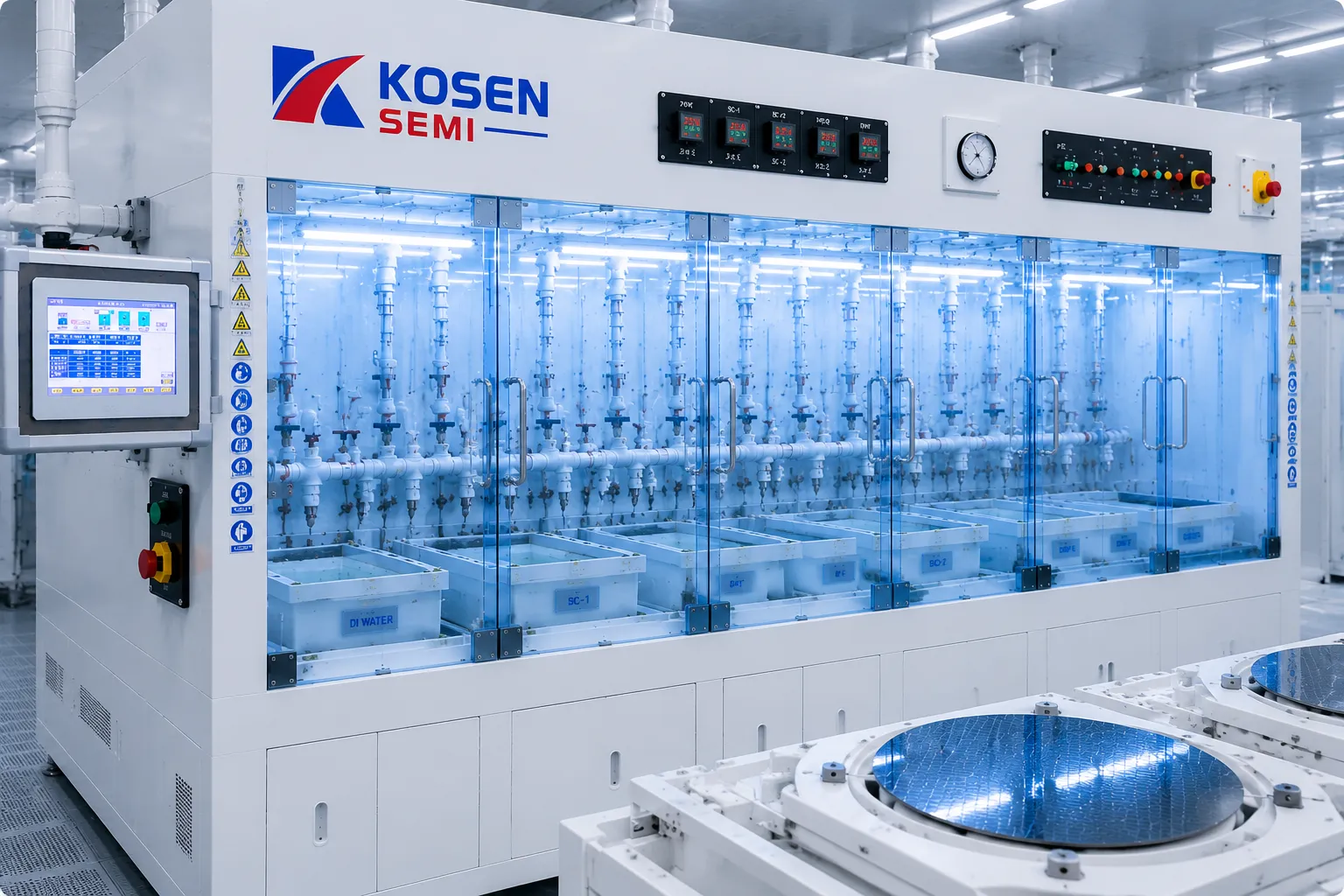
Essential Wet Etching and Cleaning Processes for Mainstream Power Devices IGBT and MOSFET
End-to-end wet processing solutions engineered for modern IGBT and power MOSFET manufacturing lifecycles. KOSEN SEMI delivers high-precision chemical etching, advanced metal lift-off, and strict contamination control through our high-performance wafer cleaning systems designed to overcome the mechanical, thermal, and surface chemistry challenges of high-power device fabrication while maximizing line yield.
Thin Wafer Backside Processing
Advanced backside spin etching and stress-relief cleaning engineered to eliminate micro-fractures, prevent wafer warping, and ensure precise thickness control on sub-100 µm substrates.
Core Technical Capabilities
- Non-Contact Bernoulli Handling: Dual-sided air-cushion wafer transport shields delicate frontside active topography during processing.
- Spin Etch Stress Relief: Controlled chemical dosing removes damaged silicon lattice layers without inducing local stress or edge chipping.
- Adaptive Warp Compensation: Dynamic edge-clamping chucks maintain planarity during high-RPM spinning for uniform etching.
- Back-Surface Oxide Stripping: Controlled residue removal supports reliable thermal and electrical contact for back metallization.
Thick Metal Etch and Lift-off Process
High-uniformity wet etching and photoresist lift-off engineered for thick aluminum, copper, and multi-layer metal stacks with precise sidewall profile control.
Core Technical Capabilities
- High-Pressure Directional Jetting: Solvent fluid dynamics penetrate tight geometries to strip cross-linked photoresist without surface staining.
- Sidewall Profile Control: Isotropic and anisotropic etching controls contact pad slopes accurately for superior step coverage.
- Anti-Redeposition Systems: Advanced inline chemical filtration prevents metallic micro-particulates and flakes from re-attaching.
- Dynamic Chemical Recirculation: In-line chemical bath management supports consistent etch rates across production runs.
High Aspect Ratio Trench Cleaning
Deep-trench polymer removal and particulate extraction tailored for trench-gate IGBTs and superjunction MOSFETs without structural wall collapse.
Core Technical Capabilities
- Megasonic Cavitation Control: Frequency-modulated physical cleaning dislodges 200 nm-class particulates, with optimized control down to 100 nm and RIE post-etch residues.
- Low Surface Tension Chemistry: Specialized surfactant formulations penetrate narrow features with aspect ratios exceeding 20:1.
- Collapse Prevention Rinsing: Surface-tension-controlled Marangoni drying sequences prevent capillary-force damage to thin silicon walls.
- Post-Etch Residue Stripping: Multi-stage chemical neutralization helps remove fluorocarbon polymers from trench sidewalls.
End-to-End Wet Processing Integration Across Power Fabrication
Mainstream power semiconductors such as insulated-gate bipolar transistors (IGBTs) and metal-oxide-semiconductor field-effect transistors (MOSFETs) demand specialized wet chemical processing. High-voltage power devices utilize deep vertical topographies, thick frontside aluminum metallization, and ultra-thin substrates designed for maximum current density and heat dissipation.
KOSEN SEMI provides fully automated wet processing tools engineered to address these operational constraints. From pre-gate oxidation cleaning to back-end thick metal lift-off and backside spin etching, our systems maintain rigorous particle control and minimal metal contamination thresholds, directly boosting breakdown voltage performance and die yield.
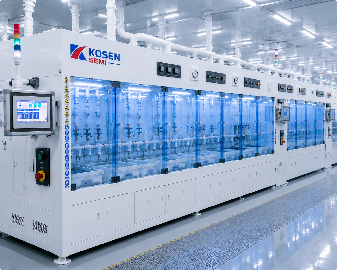
Power Device Wet Processing Specifications
| Process Step | Target Application | Primary Challenge | KOSEN SEMI Solution | Yield Impact |
|---|---|---|---|---|
| Backside Silicon Spin Etch | Thin Wafer IGBT / MOSFET | Wafer bowing, micro-cracks, uneven stress distribution | Non-contact Bernoulli chuck with real-time spin etch rate monitoring | Reduced wafer warp below 50 µm |
| Thick Al/Cu Metal Etch | Power Contact Pads | Metal redeposition, severe undercut, sidewall roughness | Temperature-controlled dynamic chemical jetting with anti-flake additives | Reduced metal residue and controlled sidewall profile |
| Deep Trench Gate Clean | Trench MOSFET & IGBT | Polymer entrapment, micro-cavitations, structural wall collapse | Frequency-modulated megasonics and low surface tension rinsing chemistry | Process-qualified polymer removal performance |
| Post-Grind Surface Clean | Back-end Substrates | Heavy silicon slurry particulate buildup | Multi-chemical scrubbing with megasonic spray manifolds | 200 nm defect minimization, optimized to 100 nm |
Flexible Equipment Architectures: Single Wafer vs. Batch Systems
Balance yield stability and production throughput with modular wet processing architectures engineered specifically for power semiconductor manufacturing, including high-efficiency wafer cleaning systems.
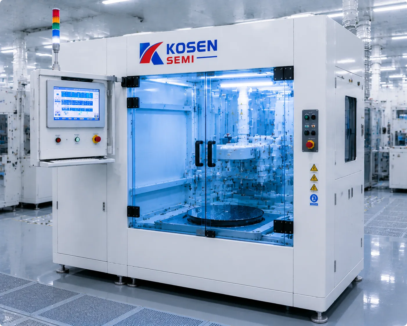
Single Wafer Processing
Delivers isolated wafer-by-wafer process control and high chemical recovery rates. Our advanced single wafer cleaning systems are optimized for high-value SiC pre-epitaxial cleaning and defect-critical steps.
- Wafer-by-wafer precision control eliminates cross-contamination
- High chemical recovery rates lower overall cost of ownership
- Optimized for high-value SiC pre-epitaxial and GaN surface prep
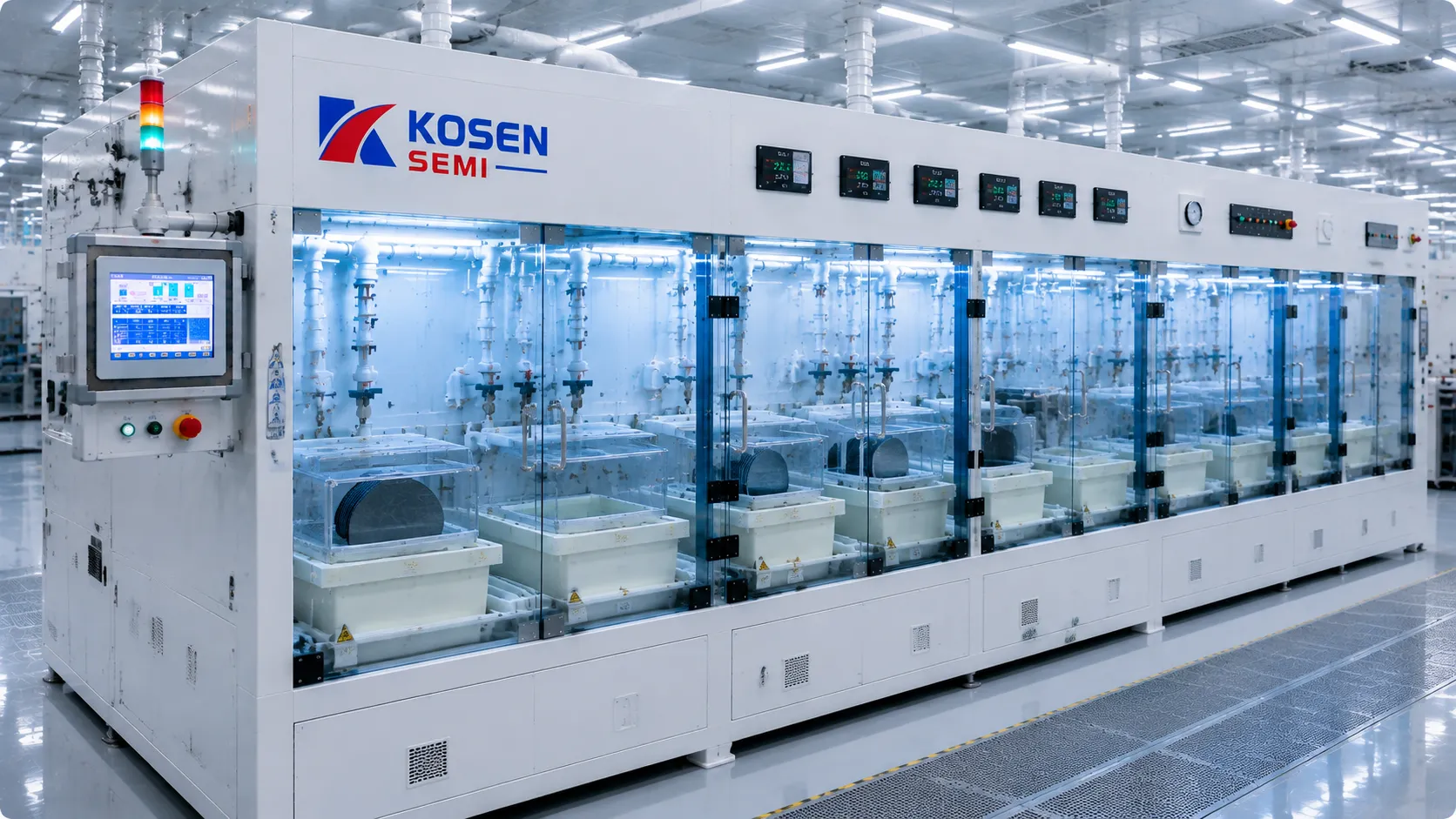
Batch Cleaning Systems
Delivers high-volume throughput and extended chemical bath lifespan. Our specialized batch wafer cleaning systems are engineered for large-scale foundational cleaning across mature power device lines.
- High-volume throughput for large-scale commercial fabs
- Extended chemical bath lifespan minimizes cost per wafer
- Ideal for foundational IGBT and MOSFET wet process stages
Architecture Technical Comparison
Match your fab operating requirements with the appropriate power semiconductor wet process architecture.
| Key Criteria | Single Wafer Systems | Batch Cleaning Systems |
|---|---|---|
| Process Control | Wafer-by-wafer isolated precision control | Multi-wafer uniform bath control |
| Chemical Efficiency | High chemical recovery and point-of-use dosing | Extended chemical bath lifespan & recirculation |
| Primary Focus | Improved yield stability and reduced cross-contamination risk | High throughput & low cost-per-wafer |
| Target Application | SiC pre-epitaxial & high-value cleaning | IGBT & MOSFET foundational cleaning |
Configure Your Equipment Architecture with KOSEN SEMI
Our semiconductor process engineering team helps you select and customize single wafer or batch architectures based on your yield and throughput goals.
Controlled Defect Reduction for High-Voltage Power Device Reliability
In power semiconductor fabrication, nanoscale particulates and trace metallic contamination severely compromise gate oxide integrity and critical breakdown voltage limits. KOSEN SEMI engineers controlled clean-chamber enclosures designed for ISO Class 5–7 cleanroom integration and dynamic anti-cross-contamination systems, supporting measurable substrate defect reduction after process qualification to safeguard high-power SiC, GaN, and silicon IGBT manufacturing yields.
Particle Control Capabilities
Eliminates high-density post-CMP slurry residue and 200 nm-class particulates, with optimized control down to 100 nm without causing surface pitting or damaging ultra-thin epitaxial structures.
atoms/cm² Threshold
Surface Metal Contamination
Enforces rigorous surface purity controls to prevent transition metal diffusion during high-temperature thermal oxidation and annealing stages.
Chemical Filtration Efficiency
Continuous point-of-use micro-filtration helps reduce re-deposited impurities and extends chemical bath operational lifespans significantly.
Fully Enclosed Clean Chamber Design
Protecting sensitive power device substrates demands isolation from ambient fab micro-environments. KOSEN SEMI builds hermetically sealed process chambers featuring positive-pressure, HEPA/ULPA-filtered laminar airflow. This isolated structural design prevents airborne molecular contamination (AMC) and environmental particulate fallout from settling on active wafer surfaces during critical wet etching and surface preparation steps in our specialized wafer cleaning systems.
Dynamic Anti-Cross-Contamination Systems
Multi-step wet chemistry sequences carry inherent risks of solution drag-out and cross-bath contamination. Our automated fluid management platforms utilize liquid barrier curtains, independent chemical delivery lines, and ultra-fast drain-and-rinse cycles to prevent cross-contamination between aggressive etching chemistries and ultra-pure water (UPW) final rinsing phases. To achieve precise target cleanliness, manufacturers rely on dedicated Single Wafer Cleaning Systems.
Substrate Defect Reduction for High-Voltage Reliability
- ✓ Protects delicate heterojunctions: Supports consistent surface condition and interface cleanliness across compatible SiC and GaN epitaxial wafers.
- ✓ Extends breakdown voltage lifespan: Eliminates metallic pinholes and micro-defects that trigger premature dielectric failure in high-power IGBTs.
- ✓ Stabilizes volume production yields: Ensures consistent, repeatable cleanliness wafer-after-wafer across demanding high-volume commercial fabs.
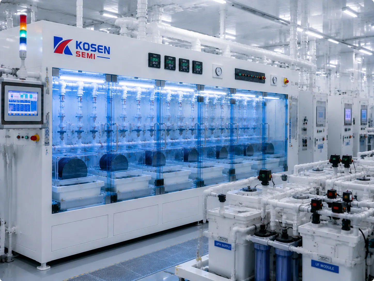
Proven Yield Protection Architecture
By combining dynamic contamination barriers with continuous chemical purification, KOSEN SEMI wet process tools support controlled defect reduction for power semiconductor manufacturing.
Frequently Asked Questions on Power Semiconductor Wet Processing
Explore detailed technical insights on chemical processing, substrate defect reduction, and critical contamination control engineered specifically for third-generation SiC, GaN, and high-power IGBT device manufacturing lines.
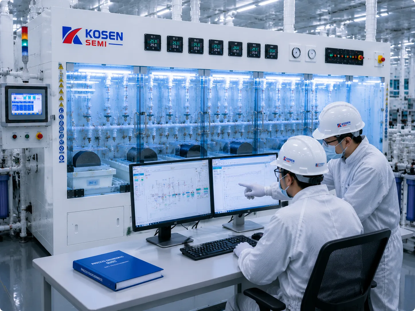
Process Engineering Support
KOSEN SEMI delivers customized wet chemical process equipment engineered for controlled defect reduction in modern power device fabrication plants worldwide.
Need customized chemical compatibility validation or sample test runs? Speak directly with our wet process engineering team.
How do KOSEN SEMI systems effectively eliminate high-hardness particulates during SiC wafer cleaning?
Silicon Carbide (SiC) substrates present extreme Mohs hardness (9.5) and high chemical inertness compared to traditional silicon. During post-CMP polishing, residual slurry particulates become deeply embedded and bound by tight van der Waals forces.
KOSEN SEMI SiC Wafer Cleaning Systems overcome this challenge through a multi-stage physical and chemical synergy:
- Targeted Megasonic Agitation: High-frequency fluid cavitation disrupts 200 nm-class particulate adhesion, with optimized control down to 100 nm without imparting structural micro-fractures into the lattice.
- High-Temperature Chemical Formulations: Customized high-concentration alkaline and peroxide mixtures (SC-1 variants) combined with specialized surfactants shift zeta potentials and lower surface tension.
- Anti-Redeposition Dynamics: Dynamic fluid replenishment mechanics ensure detached particulates are swept away immediately, maintaining high semiconductor contamination control and preventing particle re-attachment.
This integrated approach achieves particle control down to 100 nm under optimized conditions and enables reliable surface prep before critical epitaxial growth steps.
How does KOSEN SEMI handle ultra-thin power wafers under 100 microns without breakage?
High-power IGBT and MOSFET manufacturing relies on thinning wafers to under 100 microns (and down to 50 microns) to lower collector resistance and thermal impedance. At this thickness, wafers exhibit severe flexure, high fragility, and extreme warping tendencies.
KOSEN SEMI equips its wet processing platforms with dedicated thin-wafer protection mechanics:
- Bernoulli Non-Contact Chucking: Wafer transport uses non-contact airflow cushioning, eliminating mechanical stress on the wafer backside during movement.
- Edge-Exclusive Tactile Clamping: Wafer contact is restricted strictly to a 1.0 mm edge exclusion zone using soft-polymer grippers to protect delicate surface structures.
- Soft-Start Chemical Delivery: Chemical dispensing ramps smoothly in low-pressure fluid streams, mitigating acoustic shockwaves that trigger micro-fracture propagation.
These engineering innovations deliver safe, repeatable operation across thousands of continuous thin-wafer backside cleaning cycles.
What metal etching and lift-off performance can be achieved for thick metallization layers?
Thick front and backside metal layers (such as Ti/Ni/Ag or Cu stacks reaching several microns) present severe metal lift-off process challenges, including sidewall flagging, redeposition of metal flakes, and inconsistent lateral etch profiles.
KOSEN SEMI specialized IGBT wet etching and lift-off systems solve this via:
- Multi-Angle Spray Nozzle Arrays: High-impact, precision-angled solvent nozzles penetrate dense photoresist boundaries to dissolve interfaces cleanly.
- Integrated High-Efficiency Filtration: Dissolved metals and strip residues pass through continuous dynamic filtration (down to 0.1 µm), preventing recirculated metal debris from settling back onto active die areas.
- Precise Thermal Temperature Control: Chemical baths are dynamically regulated to support consistent etch rates and vertical sidewall profiles.
This helps reduce metal residue and supports consistent dielectric spacing in high-power module fabrication.
How do single-wafer processing and batch cleaning systems compare for power device scaling?
Selecting between Single Wafer Cleaning Systems and Batch Wafer Cleaning Systems depends on the target substrate material, process step criticality, and target production volume:
- Single Wafer Systems: Excel in high-value, critical steps requiring extreme wafer-to-wafer uniformity—such as SiC pre-epitaxial clean, GaN surface preparation, and high-aspect ratio trench clean. They provide isolated chemical dosing, minimal chemical cross-contamination, and precise single-side processing.
- Batch Cleaning Systems: Ideal for high-throughput, cost-sensitive foundational cleaning steps—such as pre-diffusion, post-etch RCA cleans, and high-volume IGBT substrate preparation. They process up to 50 wafers simultaneously with extended chemical bath lifespans to lower overall cost-per-wafer.
KOSEN SEMI manufactures both equipment architectures, giving power semiconductor fabs flexible options configured to their exact manufacturing roadmap.
Ready to Elevate Your Power Semiconductor Yield?
Connect directly with our senior application engineers to optimize your SiC, GaN, and IGBT wet processing lines with customized Engineering Capability for unique equipment configurations.
Defect Reduction
200 nm-class particle removal, optimized to 100 nm engineered for SiC, GaN, and high-voltage IGBT substrates.
Etch Uniformity
Precision metal lift-off and wet etch systems delivering tight process repeatability.
Custom Engineering
Tailored chemical delivery and recirculation configurations designed for your exact fab specs.
Fab-Scale Production
Scalable Single Wafer Cleaning Systems and batch platforms built to transition smoothly from R&D to mass production.
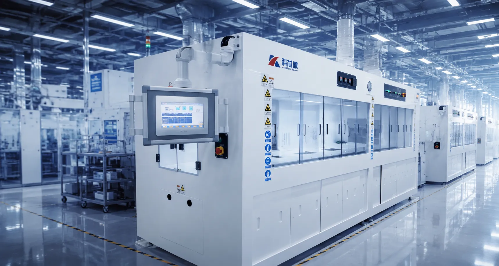
High-Yield Power Wet Process Platform
Features dynamic temperature control, megasonic cleaning via advanced wafer-cleaning-systems, and cross-contamination risk-control design.
Contact Wet Process Expert
Get specialized technical guidance and a tailored system quotation within 24 business hours.