
Semiconductor Wafer Cleaning Systems Guide
Evaluate wet vs. dry architectures, benchmark 200 nm standard particle removal with optimized capability down to 100 nm, and choose high-yield wafer cleaning systems tailored to your fab specifications.
Particle removal efficiency achieving PRE > 99% for critical node semiconductor manufacturing.
Low-damage physical cleaning compatible with ultra-thin wafers and high-aspect-ratio structures.
Eco-optimized chemical saving solutions designed to minimize cost of ownership and environmental footprint.
As a leader in semiconductor wet process equipment, KOSEN SEMI delivers high-yield wafer cleaning solutions for global Fabs and R&D institutions.
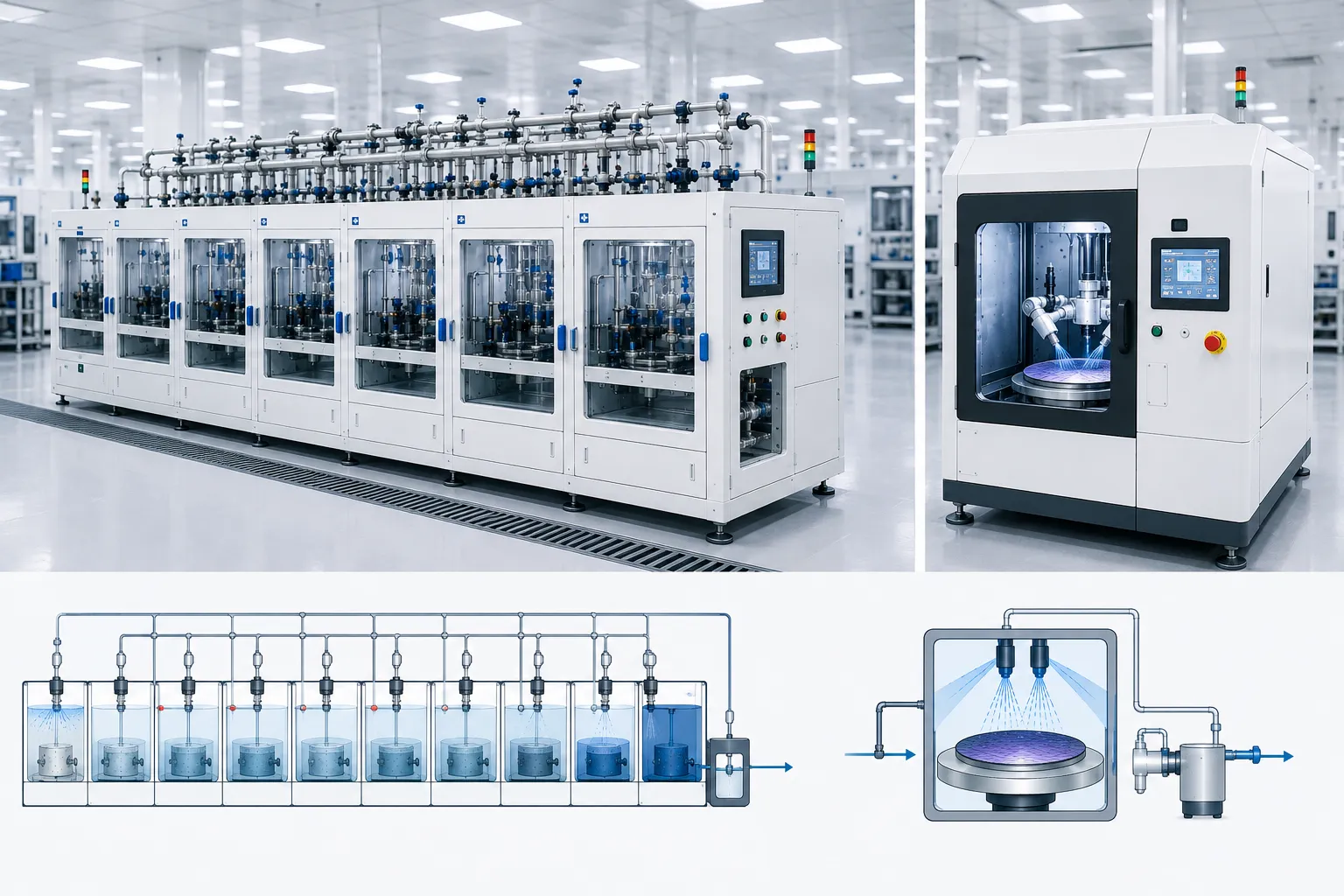
Wafer Contamination Types and Cleaning Imperative
In advanced semiconductor manufacturing, micro-contamination on substrate surfaces remains the primary driver of yield loss and device performance degradation. As critical feature dimensions shrink to advanced nanometer nodes, even particles at the 200 nm standard threshold, or down to 100 nm under optimized conditions, trace metallic impurities, thin organic films, and uncontrolled native oxides severely narrow process windows. Thoroughly analyzing wafer contamination types and deploying targeted wafer cleaning systems are imperative steps for semiconductor Fabs aiming for high-yield, low-defect fabrication.
KOSEN SEMI engineers high-performance single wafer cleaning systems and automated wet bench cleaning platforms designed for deep semiconductor defect reduction. By combining controlled physical energy with optimized chemical formulations, our platforms drive high-efficiency particle removal, trace metal extraction, and native oxide removal while protecting sensitive nanoscale patterns.
Surface Quality Analysis Before and After Cleaning
Scanning Electron Microscopy (SEM) inspection confirms high-efficiency particle removal and residue elimination across fine feature geometries within the 200 nm standard and 100 nm optimized capability range.
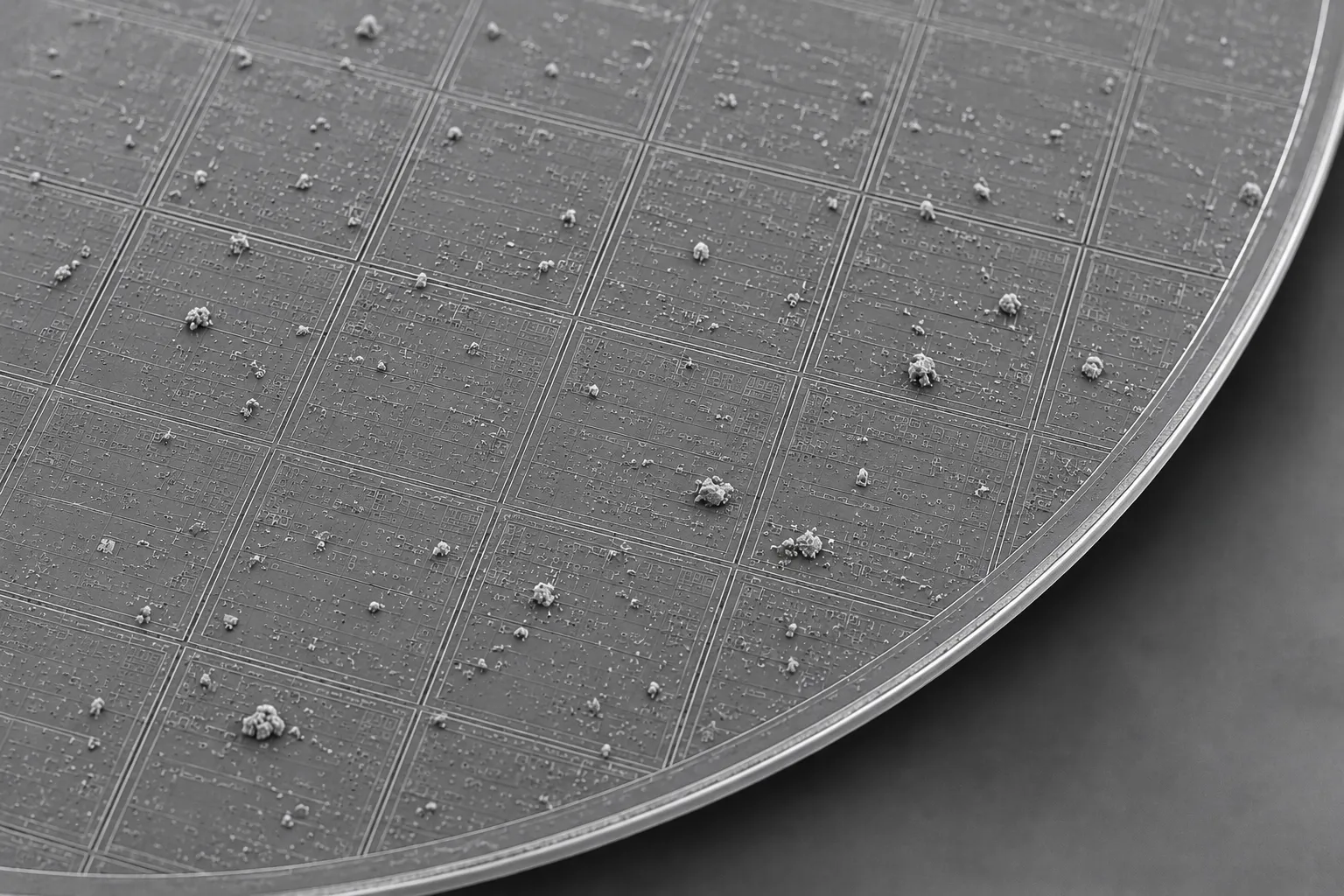 Pre-Clean State
 Contaminated Substrate Surface
High density of post-CMP slurry agglomerates, airborne particulate matter, and organic residues disrupting surface planarity prior to thermal oxidation.
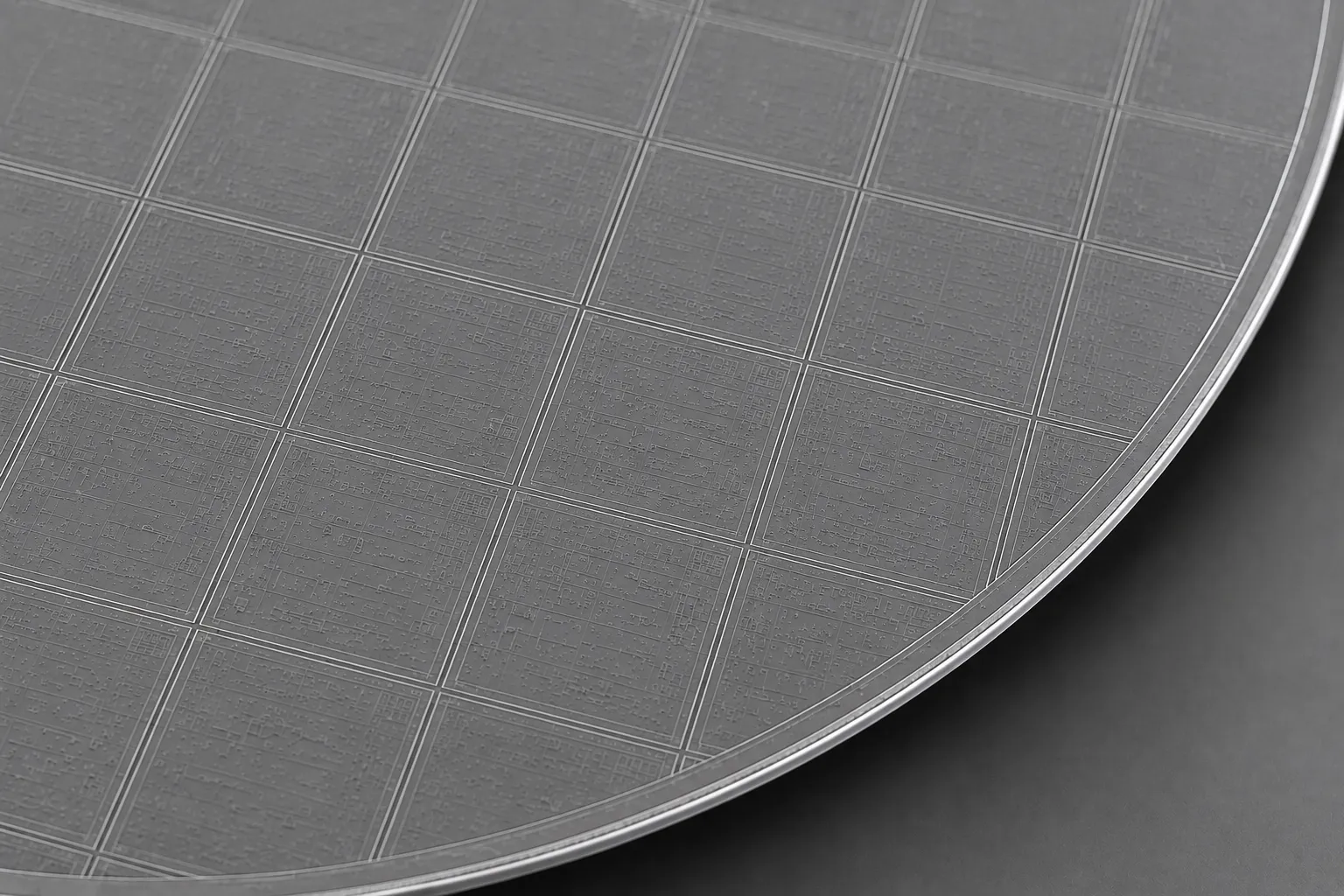 Post-Clean State
 Pristine Substrate Surface
High-efficiency particle removal and residue breakdown achieved while minimizing structural damage, surface roughening, and pattern-collapse risk on fine features.
Core Wafer Surface Contaminants Analysis
Particle Contamination
Cleanroom airborne particulates, mechanical friction from robotic end-effectors, CMP slurry agglomerates, and micro-debris from process gas delivery lines.
Post-Chemical Mechanical Planarization (CMP), post-photolithography, and dry plasma etching operations.
Causes pattern shorting, open circuits, lithographic masking shadows, and catastrophic structural defects across multi-layer interconnects.
Hydrodynamic shear force via megasonic agitation combined with SC-1 chemical conditioning to manipulate surface zeta potential, generating repulsive electrostatic forces between particles and the substrate.
Metallic Ion Contamination
Stainless steel chamber components, chemical delivery piping, ion implantation cross-contamination, and trace heavy metals (Fe, Cu, Ni, Zn) in process chemicals.
Post-ion implantation, post-high-temperature thermal annealing, and post-metal layer reactive ion etching.
Forms deep-level recombination centers in bulk silicon, reduces minority carrier lifetime, decreases gate oxide breakdown voltage, and elevates junction leakage.
Acidic complexation using SC-2 chemical mixtures or organic chelating agents that convert metallic surface species into stable, soluble ionic complexes thoroughly rinsed away by Ultra-Pure Water.
Organic Residues
Photolithography photoresist outgassing, vacuum pump oil vapors, polymeric residues from plasma etching, and FOUP plasticizer condensation.
Post-plasma ash photoresist removal, pre-gate dielectric deposition, and post-wafer dicing operations.
Inhibits uniform thin-film growth, reduces film adhesion, increases contact electrical resistance, and forms pinholes in thin gate oxide layers.
Oxidative decomposition utilizing concentrated sulfuric acid-hydrogen peroxide mixtures (SPM) or high-concentration ozonated water to break complex hydrocarbons into water-soluble compounds.
Native Oxide Film
Spontaneous silicon oxidation during ambient cleanroom exposure, residual atmospheric moisture reactions, and chemical oxidation during wet process steps.
Pre-epitaxial silicon growth, pre-silicide contact formation, and pre-atomic layer deposition (ALD) routines.
Increases interfacial contact resistance, disrupts atomic single-crystal epitaxial growth, and introduces threshold voltage variance across wafer dies.
Controlled isotropic chemical etching using dilute hydrofluoric acid (DHF) or vapor-phase HF, enabling precise native oxide removal and leaving a pristine, hydrogen-passivated silicon surface.
Comprehensive Defect Reduction with KOSEN SEMI Equipment
Effective contamination control demands precision wet processing equipment capable of adapting to varying substrate chemistries and delicate topography. Learn more about our company focus as KOSEN SEMI wafer cleaning systems integrate automated chemical dosing, uniform megasonic field distribution, and advanced Marangoni IPA drying modules to eliminate watermarks and prevent particle redeposition across advanced nodes.
- Particle Removal Efficiency (PRE) > 99.5%
- Trace metal levels < 1E10 atoms/cm²
- Low-watermark performance via Marangoni IPA drying
- Compatible with feature geometries within the 200 nm standard and 100 nm optimized capability range
Mainstream Wafer Cleaning Technologies and Process Comparison
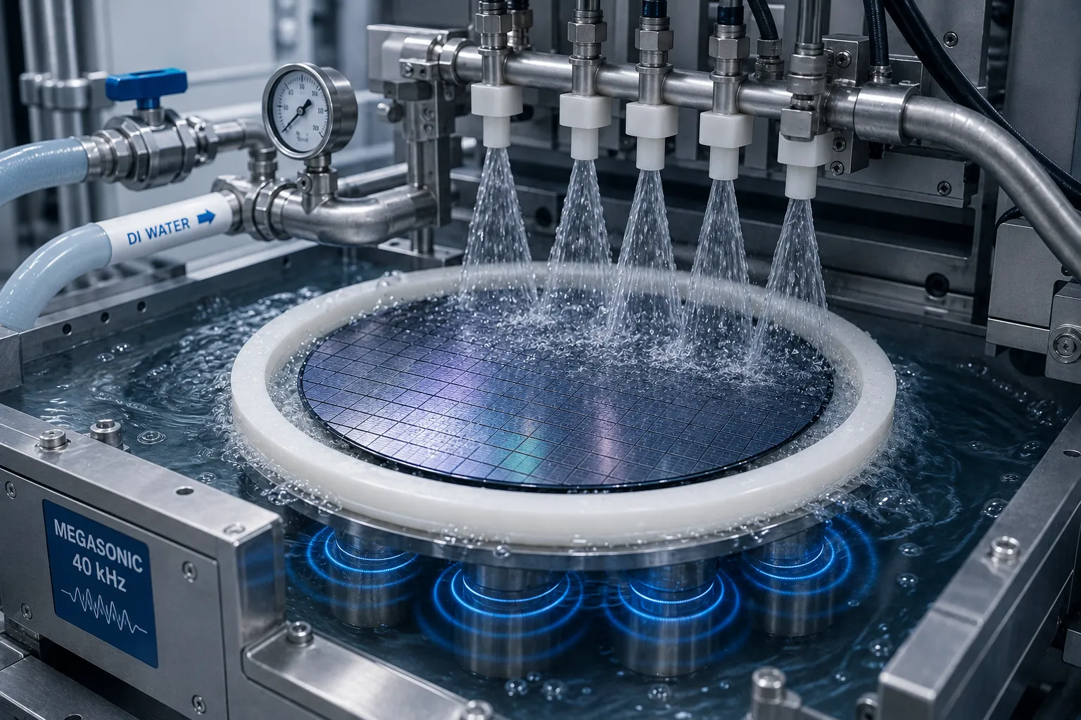
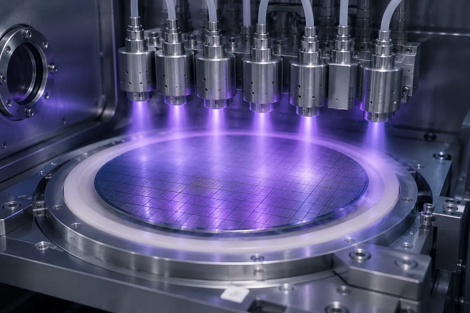
Evaluating wet wafer cleaning vs dry cleaning solutions requires a rigorous analysis of surface chemistry, micro-contamination mechanisms, and feature aspect ratios. As semiconductor manufacturing advances toward finer feature geometries, selecting the optimal surface preparation route directly determines chip yield, device reliability, and overall Cost of Ownership (COO). Standard chemical methodologies like RCA clean semiconductor setups—utilizing SC1 SC2 cleaning chemistries—must be strategically balanced against physical-assisted megasonic cleaning and dry vapor-phase etching to control particles at 200 nm under standard conditions and down to 100 nm under optimized conditions without inducing structural damage.
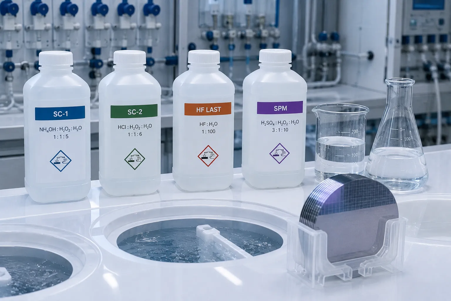
Wet Chemical Formulations: RCA Standard Cleans and SPM
Traditional wet chemical cleaning relies on controlled oxidation, etching, and metallic complexation. Refined over decades, these standard aqueous solutions dissolve organic films, strip native oxide layers, and desorb trace metallic impurities from silicon surfaces.
- Standard Clean-1 (SC-1 / APM): Formulated with ammonium hydroxide (NH4OH), hydrogen peroxide (H2O2), and deionized water (DIW) at 65°C–75°C. As the initial step in SC1 SC2 cleaning protocols, SC-1 oxidizes organic contaminants and slightly etches the substrate, inducing electrostatic zeta-potential repulsion to lift particles at 200 nm under standard conditions and down to 100 nm under optimized conditions.
- Standard Clean-2 (SC-2 / HPM): Composed of hydrochloric acid (HCl), hydrogen peroxide (H2O2), and water at 70°C–80°C. SC-2 targets alkali ions and metallic impurities (such as iron, copper, and nickel) by converting them into soluble chloride complexes, preventing re-deposition onto the bare silicon substrate.
- Sulfuric Acid Hydrogen Peroxide Mixture (SPM / Piranha): Combines concentrated H2SO4 and H2O2 at elevated temperatures (100°C–130°C). SPM serves as a potent oxidizing solution for stripping bulk photoresist layers and heavy organic polymers prior to high-temperature thermal steps.
Comprehensive Technical Parameter Comparison
Direct engineering benchmark comparing particle removal efficiency, substrate damage risks, chemical consumption, and production throughput.
| Technology Category | Primary Mechanism | PRE (standard ≥200 nm; optimized ≥100 nm) | Substrate Damage Risk | Chemical Consumption | WIP Cycle Speed |
|---|---|---|---|---|---|
| RCA Wet Chemical (SC-1 / SC-2) | Oxidation, micro-etching & complexation | Moderate (>92%) | Low (Potential native silicon loss) | High (Bulk liquid baths) | Moderate (Multi-step rinse/dry) |
| Physical-Assisted (Megasonic) | Acoustic cavitation & boundary shear flow | Ultra-High (>99%) | Minimized (KOSEN SEMI Homogenized) | Low to Moderate (Dilute chemical) | Fast (Single-wafer high RPM) |
| Anhydrous HF Vapor Etch | Gas-phase chemical surface reaction | High (Selective Oxide) | Ultra-Low (Minimized physical force) | Very Low (Precision gas dosing) | Fast (No liquid dry needed) |
| Plasma / RF Reactive Clean | Radical breakdown & volatile formation | High (Organics / Resist) | Moderate (Plasma ion bombardment) | Negligible (Gas process) | Very Fast (In-situ cluster) |
Cleaning Equipment System Architecture: Single Wafer vs Batch Wet Bench
Compare single wafer processing and wet bench system architectures to optimize wafer cleaning performance, throughput (WPH), cross-contamination control, and total cost of ownership. Explore our full range of wafer-cleaning-systems to find the ideal setup for your fab.
Single Wafer Cleaning Systems
Engineered for 200 nm standard processes with optimized capability down to 100 nm where minimized cross-contamination risk, supreme within-wafer uniformity, and precise boundary layer dynamics are mandatory.
Uses fresh, uncirculated chemistry per wafer to eliminate particle re-deposition.
Controlled spin speeds, chemical delivery, and uniform megasonic energy distribution.
Optimized for critical FEOL steps, fragile patterns, and quick recipe modifications.
- Exact chemical concentration and temperature control at single wafer level
- Rapid recipe changeovers without chemical bath reconditioning downtime
- In-situ processing monitoring with advanced IPA Marangoni spin drying
Batch Wet Bench Systems
Designed for high-throughput automated wafer washer operations, processing multiple substrate carriers in recirculating immersion tanks for maximum economic efficiency.
Simultaneous multi-wafer immersion processing delivering 500+ wafers per hour.
Recirculated, filtered chemical baths drastically reduce overall chemical consumption costs.
Optimal for 200mm/300mm mature nodes, bulk photoresist stripping, and mass pre-treatment.
- Maximum capacity utilization for high-volume 200mm and 300mm wafer fabrication
- Fully automated robotic transfer integration with SECS/GEM compliance
- Lowest total cost of ownership (COO) for continuous Giga Fab manufacturing
Architecture Trade-off Matrix: Bench vs Single Wafer Cleaning
Evaluate essential trade-offs between automated wet bench systems and single wafer tools.
Instantaneous recipe switching without shared-bath reconditioning delays.
Lowest initial equipment investment per target wafers per hour (WPH).
Eliminates bath particle accumulation and substrate-to-substrate contamination.
Fab Capacity & Architecture Evaluator
Evaluate the recommended equipment architecture based on monthly wafer starts.
Equipment Selection Decision Tree
Follow this evaluation path to match bench vs single wafer cleaning architectures with your fab metrics.
Evaluate Process Node
Determine whether device geometries require enhanced defect prevention within the 200 nm standard and 100 nm optimized capability range.
Assess Substrate & Mix
Factor in wafer size (200mm vs 300mm) and recipe variation frequency.
Target Throughput Goals
Calculate required wafers per hour for surface preparation or bulk etching.
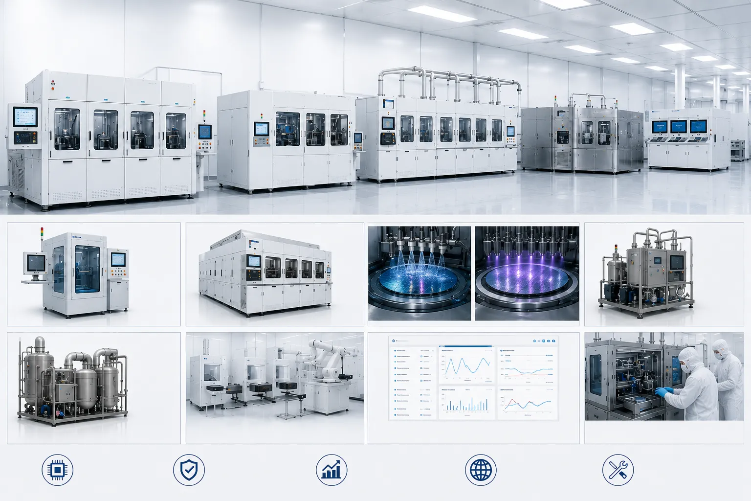
Complete Semiconductor Cleaning Architecture Portfolio
Learn more about-us to understand how we support leading fabs worldwide. We provide both high-throughput automated Wet Benches and high-precision single-wafer cleaners to meet all scenario requirements from Lab R&D to Giga Fab volume production.
Wafer Cleaning Equipment Selection: Core Evaluation Dimensions
Selecting the right wafer cleaning system is one of the highest-leverage procurement decisions in semiconductor manufacturing. The wrong choice drives up defect density, inflates chemical spend, and creates integration headaches that persist for years. This guide breaks down the three critical evaluation dimensions every engineering and procurement team must assess — plus a procurement trap that routinely derails otherwise well-specified projects.
KOSEN SEMI's engineering team designs every platform to strict SEMI value-add standards, giving customers a structured path to minimize total Cost of Ownership (COO) across the full equipment lifetime. Use the checklist below as your baseline evaluation framework for technical and commercial validation.
Process Compatibility
Chemical resistance and bath material selection directly determine whether your equipment survives aggressive process chemistries at elevated temperatures without contaminating the wafer surface.
- Bath material grade: Confirm high-purity PFA, PVDF, or quartz construction matched to your exact chemical set (HF, H₂SO₄/H₂O₂, SC-1, SC-2, ozone DIW) to ensure chemical compatibility.
- Temperature control precision: Verify ±0.5°C or better precision for SPM and heated SC-1 baths; thermal uniformity across the bath volume prevents non-uniform etch rates.
- Chemical compatibility matrix: Request a full materials-of-construction datasheet and cross-reference against all wet chemistry steps, including aggressive roadmap cleaning agents.
- Native oxide removal capability: Confirm dilute HF or vapor-phase HF integration for pre-gate oxide and pre-epitaxial cleans demanding sub-angstrom interface control.
- Substrate versatility: Ensure compatibility with Silicon, SiC, GaN, MEMS, and glass substrates if your production facility supports compound semiconductors or advanced packaging.
Automation and Cleanliness
Automation level and mini-environment cleanliness class are the primary determinants of within-wafer uniformity and lot-to-lot repeatability — especially critical at optimized 100 nm process conditions.
- Clean mini-environment: Use an ISO Class 5–7 internal environment with ULPA filtration and positive-pressure N₂/air purge to reduce airborne particle recontamination risk.
- Robotic arm transfer precision: Specify end-effector repeatability (±0.1mm or better) and confirm smooth handling across 200mm and 300mm FOUP/FOSB carrier configurations.
- SECS/GEM protocol support: Ensure full SEMI E5/E30 compliance for seamless MES integration, recipe automation, remote alarm reporting, and inline SPC monitoring.
- Process monitoring & analytics: Look for real-time concentration sensors, acoustic power monitors, and particle counter feedback loops for instant out-of-spec correction.
- Cross-contamination prevention: Require dedicated chemical fluidic lines, non-contact edge handling, and N₂ barrier purges to prevent cross-lot chemical carryover.
Cost of Ownership and Sustainability
Capital cost is only a fraction of total semiconductor COO. Chemical consumption, DI water usage, exhaust treatment, and maintenance intervals compound over a 10-year equipment lifetime.
- Chemical recycling loop system: Evaluate closed-loop bath recirculation and chemical spikes to cut virgin chemical consumption by up to 40% compared to open drain designs.
- DI water consumption per wafer: Request normalized DI water usage metrics (L/wafer); counter-current rinsing and quick-dump rinse (QDR) optimization can reduce DI water cost by 30%+.
- Exhaust treatment & abatement: Confirm point-of-use acid exhaust scrubbing and VOC containment features to satisfy stringent cleanroom safety and environmental compliance standards.
- Preventive maintenance (PM) intervals: Long mean-time-between-failures (MTBF) and short mean-time-to-repair (MTTR) reduce unscheduled fab downtime and lower long-term COO.
- Energy efficiency benchmarking: Compare electrical consumption (kWh/wafer) across heating modules, chilling units, and high-flow N₂ dry cycles to minimize baseline utility overhead. Our corporate focus on sustainability ensures every platform helps reduce overall fab emission goals.
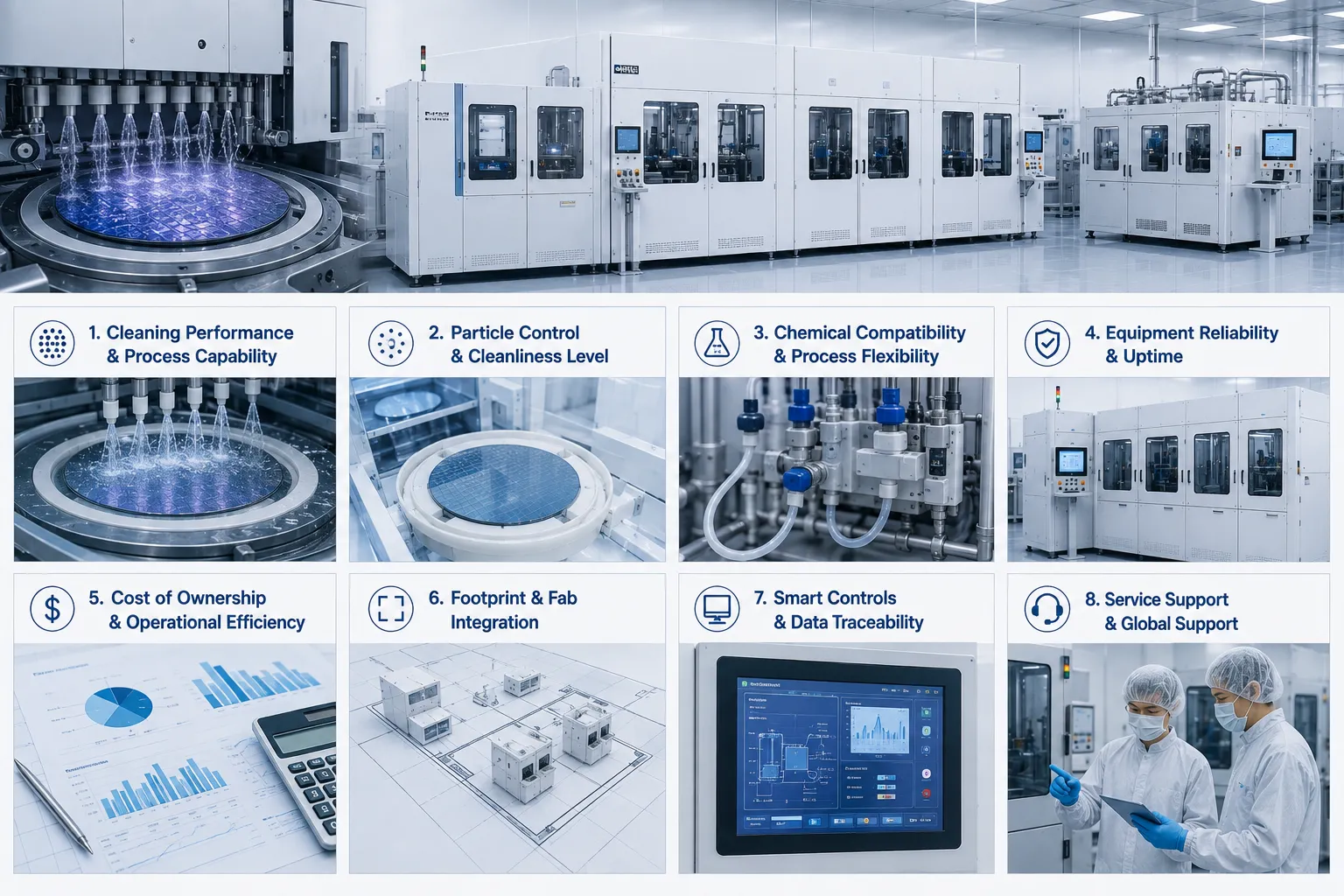
How to Apply This Wafer Cleaning Equipment Selection Framework
Effective wafer cleaning equipment selection requires balancing immediate process performance requirements against long-term operational expenses. Process engineers must weight each evaluation dimension based on wafer diameter (200mm vs. 300mm), target technology node, line throughput targets, and specific surface chemical tolerances.
When requesting vendor specifications, always demand empirical performance data under real production conditions—including particle removal efficiency (PRE) for particles at 200 nm under standard conditions and down to 100 nm under optimized conditions, trace metal contamination levels (< 1x10¹⁰ atoms/cm²), and exact chemical delivery control limits. Calculating realistic semiconductor COO models early in the RFP phase ensures capital allocation yields maximum return and lowest total cost over the tool's 10-to-15 year operational lifespan.
Procurement Trap Warning: Inadequate Drying & Watermark Defect Vulnerability
Evaluating chemical resistance and bath materials is essential, but neglecting post-clean drying mechanics is one of the most frequent mistakes made during wafer cleaning equipment selection. Standard spin-drying or basic nitrogen blow-off methods often leave microscopic liquid droplets behind on hydrophobic silicon surfaces or deep high-aspect-ratio trench patterns. As these droplets evaporate, residual silica and chemical impurities precipitate out, forming catastrophic watermark defects that destroy device yields.
KOSEN SEMI solves this issue by integrating advanced IPA Marangoni drying and surface tension gradient technologies across our automated single wafer cleaning systems and batch wet platforms. By establishing a ultra-clean IPA/N₂ vapor interface during fluid displacement, our equipment minimizes watermark formation and structural pattern-collapse risk—securing baseline yield stability on critical semiconductor structures.
Precision Wafer Cleaning Solutions Across Every Manufacturing Stage
From front-end transistor fabrication to advanced back-end packaging, KOSEN SEMI provides application-tailored contamination control through advanced wafer-cleaning-systems to maximize yields across all substrate types.
FEOL Front-End Cleaning
Achieves critical particle and trace metal removal for pre-gate oxide cleaning, post-ion implantation photoresist stripping, and SPM ash residue removal using high-precision Single Wafer Cleaning Systems.
Multi-frequency megasonic soundfields paired with targeted chemical spray dispense modules deliver PRE > 99% with minimized substrate erosion.
BEOL Back-End Cleaning
Removes organic slurries and metallic residues following Cu CMP while preparing contact pads for reliable wire bonding and passivation.
Dual-sided soft PVA brush scrubbing integrated with specialized chelating chemical dispense protects delicate interconnect lines.
Advanced Packaging & TSV
Delivers deep silicon via (TSV) particle evacuation and precise surface treatment before micro-bump plating for 2.5D/3D IC integration.
Focused acoustic energy penetration paired with low-surface-tension chemistry flushes particles within the 200 nm standard and 100 nm optimized control range from deep structures.
Compound Semi & MEMS
Supports high-yield SiC and GaN substrate cleaning along with gentle, stiction-free drying for micro-mechanical structure release.
Gentle chemical delivery combined with IPA Marangoni or supercritical drying eliminates pattern collapse on fragile MEMS features.
Production-Proven Cleaning Parameter Configurations
Whether processing Silicon, SiC/GaN, or Glass substrates, KOSEN SEMI leverage robust Engineering Capability to provide proven process recipe configurations backed by extensive fab data to streamline your production rollout.
Frequently Asked Questions: Wafer Cleaning Systems
These engineering answers address the most critical technical and procurement questions fab managers and process integration teams ask when evaluating semiconductor wafer cleaning equipment. From pattern collapse prevention in high-aspect-ratio (HAR) features to SECS/GEM MES integration, each insight reflects real-world fab experience aimed at accelerating qualification and maximizing wafer cleaning yield optimization.
Pattern collapse in HAR structures—such as fin arrays, 3D NAND deep contact holes, and fine gate-stack structures—is primarily triggered by capillary forces at the liquid-vapor interface during wafer drying. As the rinsing liquid evaporates, surface tension creates asymmetric capillary pressure that pulls adjacent features together, causing permanent structural collapse and catastrophic line-bending defects.
Key mitigation strategies for advanced semiconductor nodes include:
- IPA Marangoni Drying: Introducing a controlled isopropyl alcohol (IPA) vapor gradient displaces Deionized Water (DIW) from the wafer surface without a receding liquid meniscus. This eliminates capillary forces and prevents collapse on structures with aspect ratios exceeding 10:1.
- Supercritical CO₂ (scCO₂) Drying: For extreme HAR architectures (aspect ratios > 30:1), transitioning directly from liquid to supercritical phase bypasses phase boundaries entirely, resulting in no liquid-gas phase boundary and minimized collapse risk.
- Surfactant & Low-Surface-Tension Chemistries: Incorporating specialized chemical additives or dilute solvent rinses lowers liquid surface tension during the final wet processing step, mitigating capillary stress prior to drying.
- Optimized Acoustic & Megasonic Energy: Tuning megasonic power density and frequency (typically 0.8–1.0 MHz) prevents mechanical deflection of fragile structures during wet particle removal.
System architecture also plays a vital role: single-wafer cleaning tools with closed-loop spin speed and precise IPA vapor dispensation provide superior drying repeatability compared to conventional batch wet benches. KOSEN SEMI's process engineering team conducts comprehensive SEM cross-sectional defect analysis to tailor drying protocols and prevent pattern collapse across advanced feature geometries.
Need tailored technical advice or process validation?
Our process lab features dozens of senior semiconductor cleaning experts with extensive Engineering Capability available at any time to provide customers with process diagnostics and parameter optimization support.
Ready to elevate your wafer cleaning yield and process stability?
Schedule a process lab consultation with KOSEN SEMI engineers. Test custom wafer-cleaning-systems capabilities on your production substrates to accelerate 200 nm standard defect reduction with optimized capability down to 100 nm.
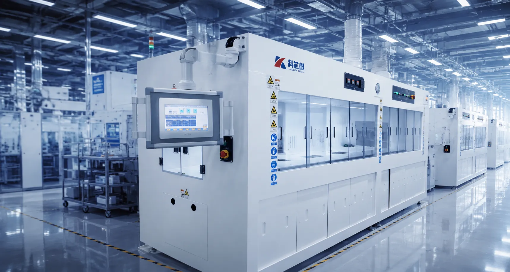 Process Verification Laboratory
 Wafer Demo Cleaning Test
Validate real-world particle removal efficiency (PRE > 99%) on your production substrates with advanced Single Wafer Cleaning Systems.
Micro-Contamination Analysis Reports
Receive precise pre- and post-clean particle counts and surface defect evaluations.
Customized Equipment Selection Plans
Obtain modular tool configurations backed by our team's world-class Engineering Capability and chemistry recipes tailored to your target fab yield.
Schedule Demo Cleaning
Submit your wafer demo cleaning test details for immediate application engineering feedback.