
High-Precision Optoelectronic Manufacturing & Precision Cleaning Solutions
Low-damage, ultra-clean wet processing and surface contamination control systems engineered by KOSEN SEMI for photonics, LEDs, laser diodes, and photodetectors. Learn more about us and our specialized industry solutions.
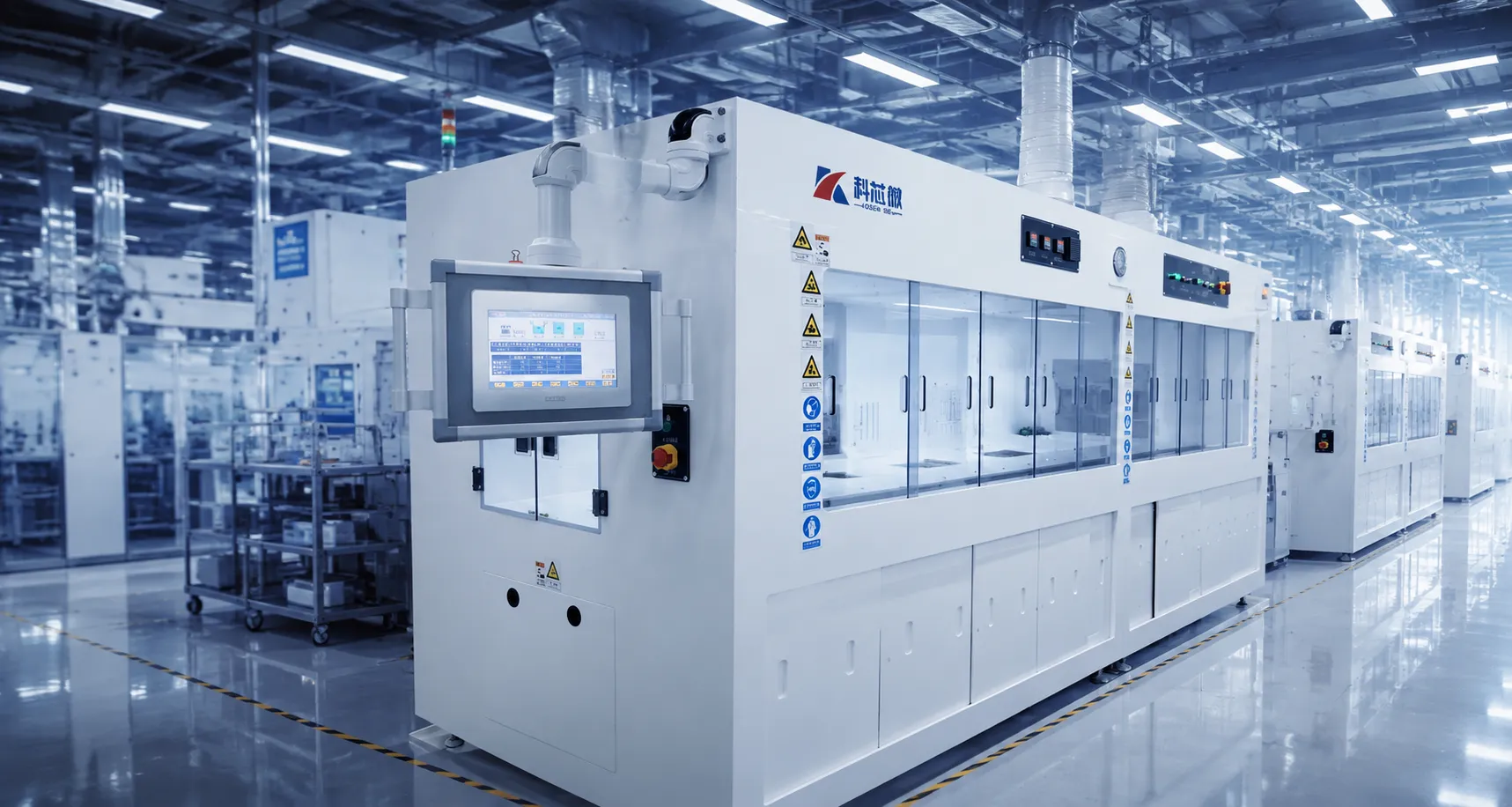
Precision Wet Processing for Optoelectronic Applications
Engineered contamination control and wet etching solutions optimized for compound semiconductors, micro-displays, and high-frequency photonic devices.
Laser Facet Cleansing & Epitaxial Surface Prep
Consistent facet cleaning and controlled surface preparation across supported wet fabrication stages.
- End-Facet Oxidation Control: Specialized chemical bath formulations eliminate native oxides without micro-trenching optical mirror facets.
- Epitaxial Wafer Precision Cleaning: Megasonic-assisted chemical agitation dislodges 200 nm-class particulates, with optimized removal down to 100 nm from delicate epitaxial layers.
- Non-Destructive Chemical Stripping: Gentle photoresist stripping tailored for fragile compound wafer geometries and delicate structures.
LED Substrate Cleaning & Pre-LLO Preparation
Ultra-clean surface preparation tailored for high-density LED arrays prior to Laser Lift-Off (LLO) and high-yield mass transfer processes.
- Pre-LLO Contamination Removal: Strips organic thin films and ionic particulates to eliminate thermal trapping during laser ablation.
- Mass Transfer Surface Prep: Controlled surface preparation helps improve micro-die pickup consistency and downstream transfer yield.
- High-Throughput Batch Processing: Automated wet benches optimize LED substrate throughput while preventing cross-contamination.
Photodetector Surface Preparation & Wet Etching
Controlled wet chemical etching and residue removal systems engineered for optical sensors, CIS arrays, and avalanche photodiode (APD) structures.
- Controlled Chemical Etching: Highly uniform etch rate control across photodetector active areas to maintain optical response uniformity.
- Chemical Residue Removal: Complete stripping of hard-baked photoresists, polymer residues, and trace metallic impurities.
- Dark Current Suppression: Atomic-scale photodetector surface preparation reduces surface trap states and minimizes noise.
Silicon Photonics & III-V Cross-Interface Cleaning
Multi-material surface decontamination engineered for heterogeneously integrated III-V light sources on silicon photonic (SiPh) interposers.
- Hybrid Bonding Surface Prep: Achieves controlled-particle interfaces required for seamless direct wafer-to-wafer bonding without voiding.
- Waveguide Structure Protection: High-frequency Megasonic flow fields safeguard delicate sub-micron optical waveguides.
- Selective Oxide Removal: Targeted chemical bath systems strip native oxides while preserving underlying silicon and compound structures.
Ultra-Thin Wafer Surface Passivation & Etching
Non-destructive wet processing for fragile, ultra-thin compound semiconductor substrates prone to mechanical shear and chemical degradation.
- Fragile Substrate Handling: Non-contact Bernoulli handling techniques prevent micro-fractures in sub-100 µm InP and GaAs wafers.
- Atomic Surface Smoothness: Precise chemical delivery supports consistent surface preparation prior to epitaxy or passivation.
- Hazardous Chemistry Containment: Enclosed, automated exhaust systems safely manage aggressive III-V wet chemical formulations.
Precision Cleaning for Micro-Gratings & Optics
Advanced chemical cleaning and IPA Marangoni drying engineered for diffractive optical elements (DOE), micro-gratings, and beam splitters.
- Stain-Free IPA Drying: Vapor Marangoni drying mechanism eliminates surface tension gradients to prevent drying stains and micro-watermarks.
- Deep Cavity Penetration: Cavitation-controlled micro-bubble agitation dislodges trapped particulates in narrow optical grooves.
- Optical Transmittance Preservation: Supports high optical cleanliness while minimizing impact on compatible anti-reflective or dielectric coatings.
Solving Complex Optoelectronic Manufacturing & Yield Challenges
Manufacturing next-generation optoelectronic devices requires balancing aggressive chemical residue removal with extreme physical structural protection. Unlike conventional silicon CMOS, compound semiconductors such as Gallium Arsenide (GaAs) and Indium Phosphide (InP) are mechanically fragile and highly susceptible to unwanted oxidation. KOSEN SEMI wet processing platforms are custom-engineered to navigate these unique material constraints, combining real-time chemical concentration control, uniform fluid dynamics, and non-destructive acoustic energy for maximum process control and yield enhancement.
| Device Family | Critical Manufacturing Challenge | KOSEN SEMI Wet Process Solution | Measurable Yield Impact |
|---|---|---|---|
| Laser Diodes (EEL / VCSEL) | End-facet oxidation & particulate light scattering | Low-damage laser diode wet processing with nitrogen purge drying | Up to 99.4% facet yield rate |
| Micro-LED & Mini-LED | Substrate lift-off residue & mass transfer defects | High-purity LED substrate cleaning with ultrasonic fluidic agitation | 40% reduction in transfer defect density |
| Photodetectors (APD / CIS) | Polymer residues & dark current surface states | Anisotropic chemical etch & photodetector surface preparation | Sub-0.1 nA dark current noise floor |
| Silicon Photonics (SiPh / III-V) | Cross-interface voids during hybrid direct bonding | 200 nm particle removal, optimized to 100 nm with IPA Marangoni drying | Near-zero void direct bonding interfaces |
Non-Destructive 200 nm Particle Removal, Optimized to 100 nm
Conventional high-pressure spray delivery can easily damage fragile micro-structures, such as micro-cantilevers or high-aspect-ratio optical waveguides. KOSEN SEMI utilizes multi-frequency Megasonic transducers calibrated to generate controlled cavitation micro-bubbles. This gentle acoustic kinetic energy dislodges 200 nm-class particulates, with optimized removal down to 100 nm without inducing structural stress or crystalline lattice damage.
Precision Surface Chemistry & Stain-Free Drying
Residual watermarks and chemical stains on optical surfaces introduce unwanted light scattering and signal attenuation. Our automated wet processing benches integrate closed-loop chemical monitoring with advanced IPA Marangoni vapor drying. By eliminating surface tension gradients during wafer lift, optoelectronic substrates emerge dry with controlled particle levels, ready for immediate optical coating or packaging.
Advanced 200 nm Defect Control, Optimized to 100 nm for Optoelectronic Substrates
Achieving maximum die yield across high-frequency laser diodes, Micro-LED arrays, photodetectors, and silicon photonics demands complete 200 nm-class defect control, optimized to 100 nm without inducing mechanical or structural damage. KOSEN SEMI combines precision fluid dynamics, megasonic acoustic fields, closed-loop chemical dosing, and surface-tension-free drying into specialized wafer cleaning systems tailored for delicate optoelectronic devices.
200 nm Particle Removal, Optimized to 100 nm via Megasonic Acoustic Streaming
Sensitive optical waveguides, gratings, and delicate micro-cantilevers cannot tolerate aggressive physical scrubbing. KOSEN SEMI engineered a specialized 200 nm particle removal framework, optimized to 100 nm utilizing multi-frequency megasonic acoustic streaming paired with controlled micro-bubble cavitation. This mechanism dislodges 200 nm-class contaminants, with optimized removal down to 100 nm without imposing physical strain or causing micro-fractures on fragile optoelectronic features.
- Controlled acoustic cavitation regulates power density to prevent standing-wave hot spots and avoid structural stress across thin compound semiconductor wafers.
- High particle removal efficiency achieves exceeding 99.8% PRE on 200 nm-class particulate contamination across patterned and unpatterned surfaces.
- Uniform fluid acoustic coupling ensures consistent physical cleaning energy across 2-inch to 8-inch compound and silicon photonics substrates.
Key Benefit: Eliminates yield-critical particulate contamination on active optical facets and waveguides without physical surface contact.
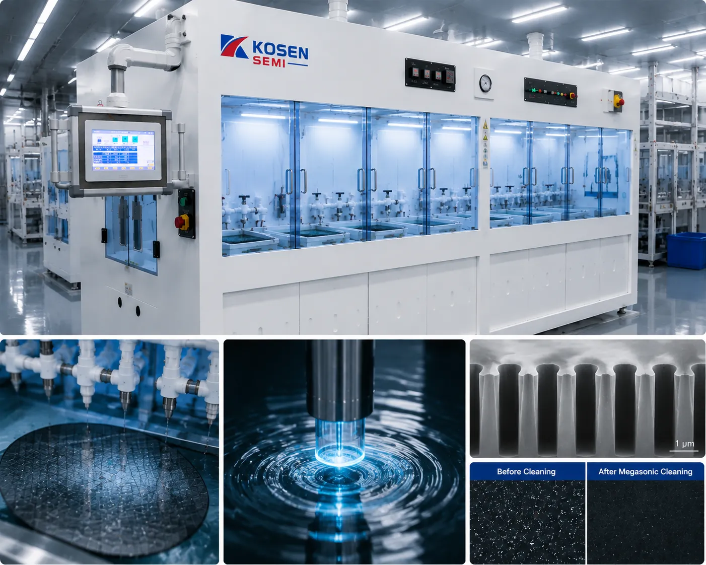
System Feature
Megasonic Micro-Bubble Cavitation Module
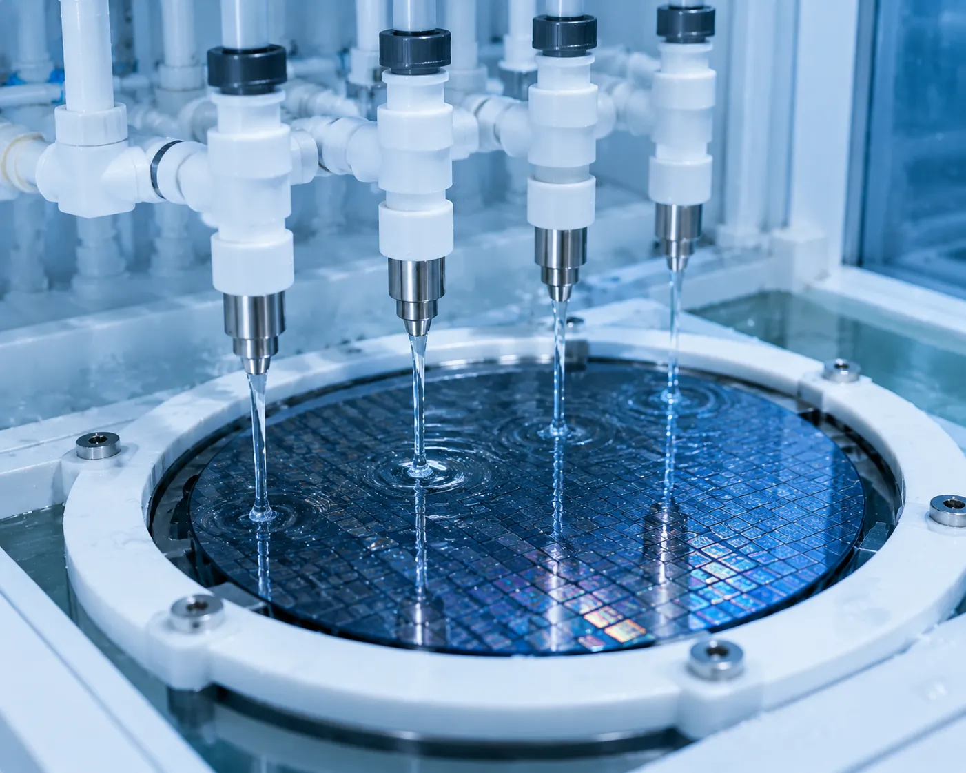
Process Feature
Ultra-Clean Wet Etch & Dosing Unit
Low-Damage Chemical Processing & Ultra-Clean Wet Etch
Precision compound semiconductor substrates such as GaAs, InP, GaN, and silicon photonics require ultra-gentle chemical processing. KOSEN SEMI's ultra-clean wet etch equipment maintains tight chemical concentration limits and precise isothermal control. This supports uniform material removal across active quantum wells and epitaxial thin films while preventing chemical pitting and unwanted surface oxidation.
- Closed-loop chemical dosing maintains bath stoichiometry within ±0.05% concentration limits for highly repeatable wet etching performance.
- Isothermal thermal management regulates process liquid temperature to within ±0.1°C to protect sensitive device structures.
- In-situ dissolved oxygen suppression prevents surface re-oxidation on reactive III-V compound interfaces during processing.
Key Benefit: Delivers stable wet-process control and consistent chemical surface preparation across supported compound semiconductor materials.
High-Uniformity Surface Drying with Low-Watermark Retention
Surface tension during conventional spin-drying causes pattern collapse and leaves watermark stains on dense optical microstructures. KOSEN SEMI integrates advanced IPA Marangoni drying and Supercritical CO2 drying capabilities directly into the optoelectronic wet processing workflow. By eliminating liquid phase boundaries, high-aspect-ratio optical gratings are preserved and drying stains are eliminated.
- IPA Marangoni drying mechanism creates controlled surface tension gradients that pull liquid films cleanly off substrate surfaces.
- Supercritical CO2 drying option bypasses liquid-gas phase interfaces to completely prevent pattern collapse on micro-sensors and photonic structures.
- Residue-free drying performance supports light extraction performance and consistent downstream optical coating adhesion.
Key Benefit: Supports optically clean substrate surfaces with reduced watermark and residue risk.
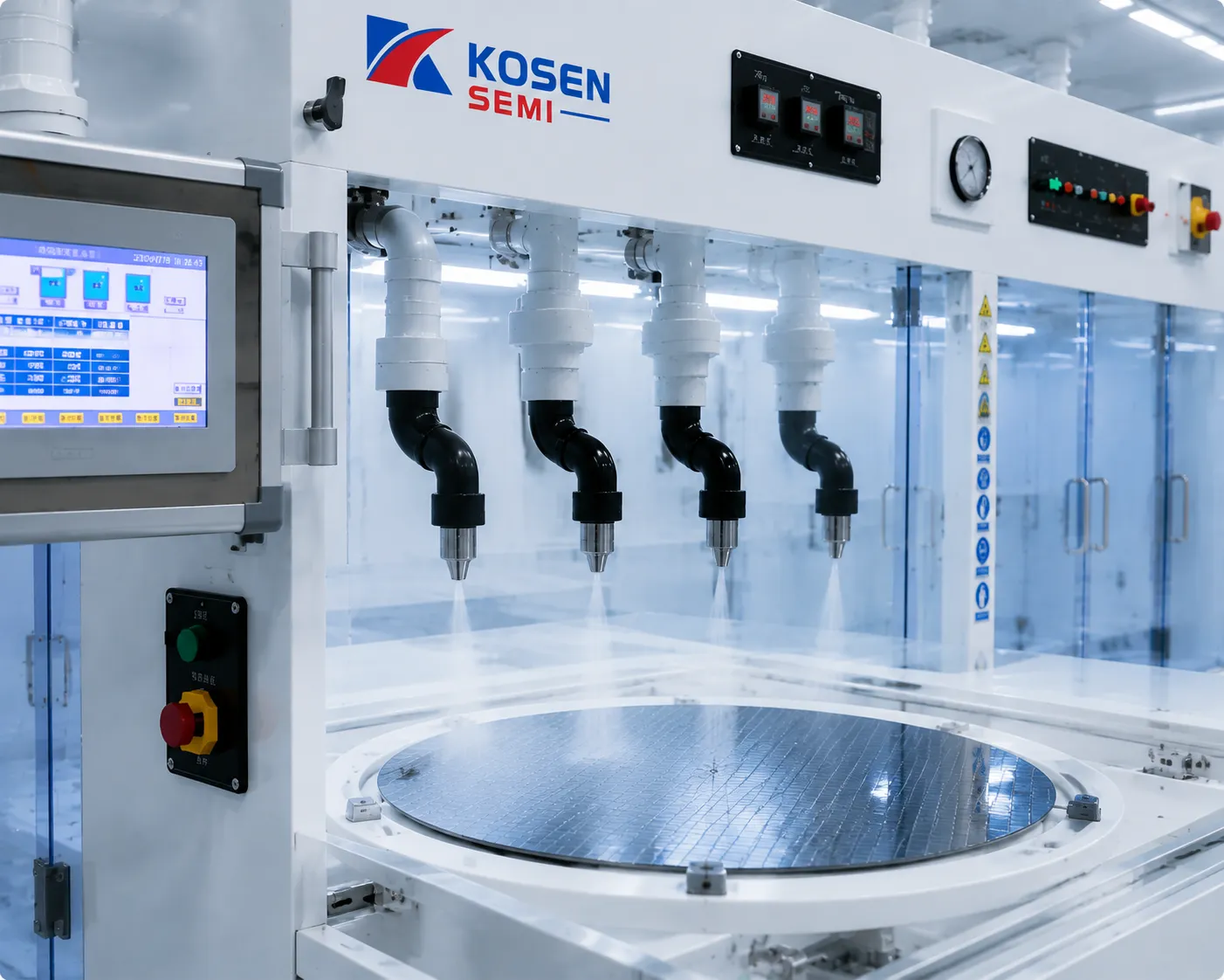
Drying Module
IPA Marangoni Drying Chamber
Process Performance Benchmarks
Comparison of key process metrics achieved by KOSEN SEMI advanced wet process technology versus legacy optoelectronic cleaning methods.
| Process Parameter | Legacy Wet Processing | KOSEN SEMI Platform | Impact on Device Yield |
|---|---|---|---|
| 200 nm Particle Removal, Optimized to 100 nm | 78.0% – 85.0% PRE | 99.8% PRE | Eliminates optical scattering and facet defects to increase light output efficiency. |
| Micro-Structure Mechanical Damage | 2.0% – 4.5% Fracture Rate | 0.0% Structural Damage | Prevents pattern collapse on fragile cantilevers and high-aspect-ratio gratings. |
| Wet Etch Depth Uniformity | ±5.0% Deviation | ±0.8% Deviation | Ensures exact optical resonance wavelengths and uniform quantum well thickness. |
| Watermark Stain Incidence | Frequent on fine grids | Low-Watermarks | Enhances thin-film coating adhesion and downstream wire bonding reliability. |
Specialized Optoelectronic Wet Processing Equipment & System Selection
Match your substrate size, throughput demands, and process parameters with KOSEN SEMI high-precision optoelectronic wet processing equipment. From pilot-line R&D tools to scalable, fully automated wafer cleaning systems, our platforms deliver controlled 200 nm particle performance, optimized to 100 nm and surface integrity. Learn more about our company mission on our about-us page.
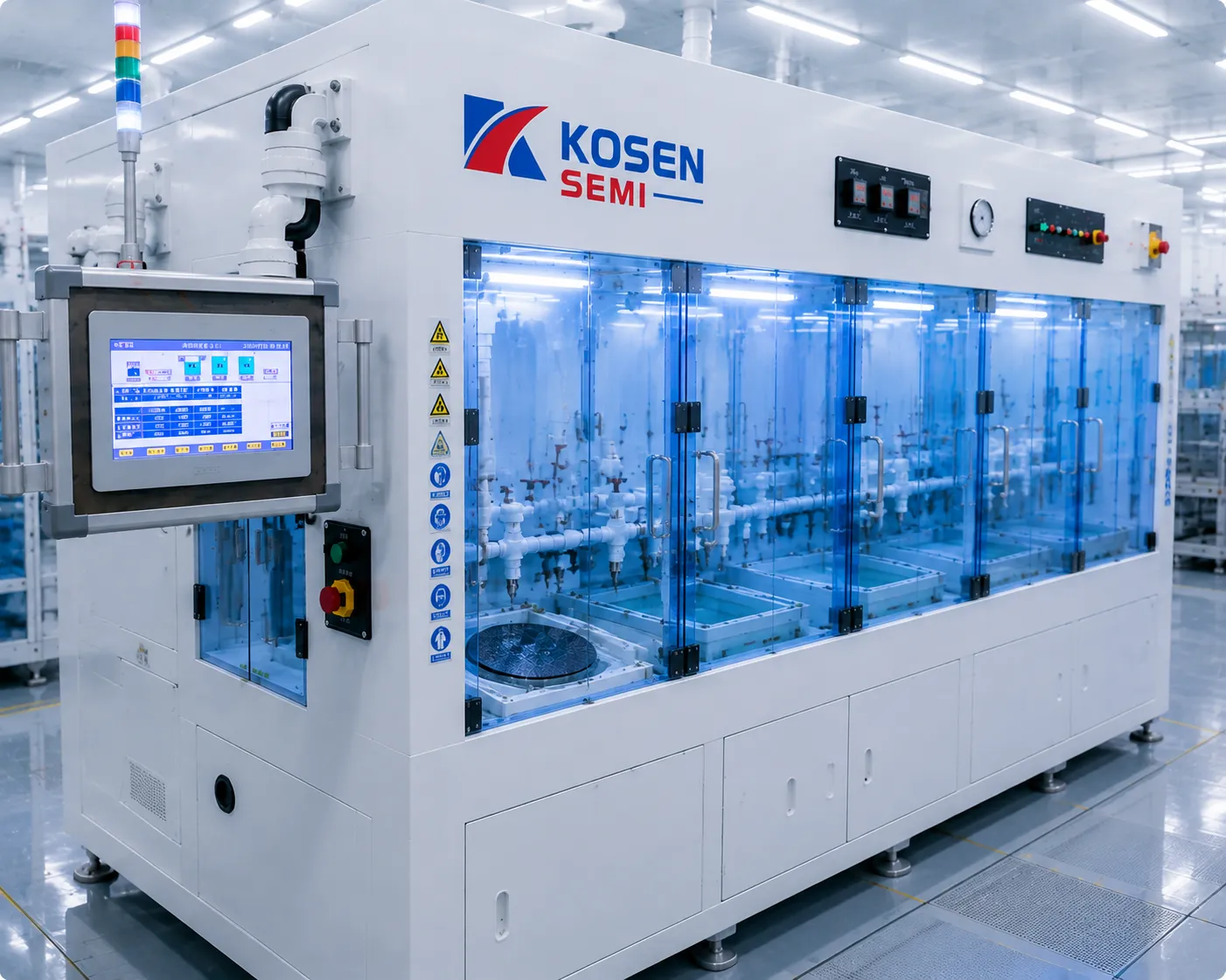
Fully Automated Single-Wafer Optoelectronic Cleaner
Engineered for high-value laser diode bars, silicon photonics, and delicate III-V substrates. This automated wafer cleaning system delivers single-wafer non-contact megasonic agitation and targeted chemical dispense without physical surface damage.
- Substrate Size
- 2–8 Inch Wafer
- Target Device
- Laser Diodes & PICs
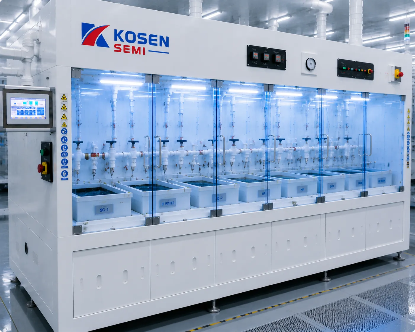
Multi-Tank Batch Wet Bench Station
Optimized for high-throughput LED substrate cleaning and compound semiconductor processing. Features automated robotic transfer, continuous chemical recirculation, auto-dosing, and specialized overflow rinse baths.
- Substrate Size
- 2–8 Inch Wafer
- Target Device
- Micro-LED & Substrates
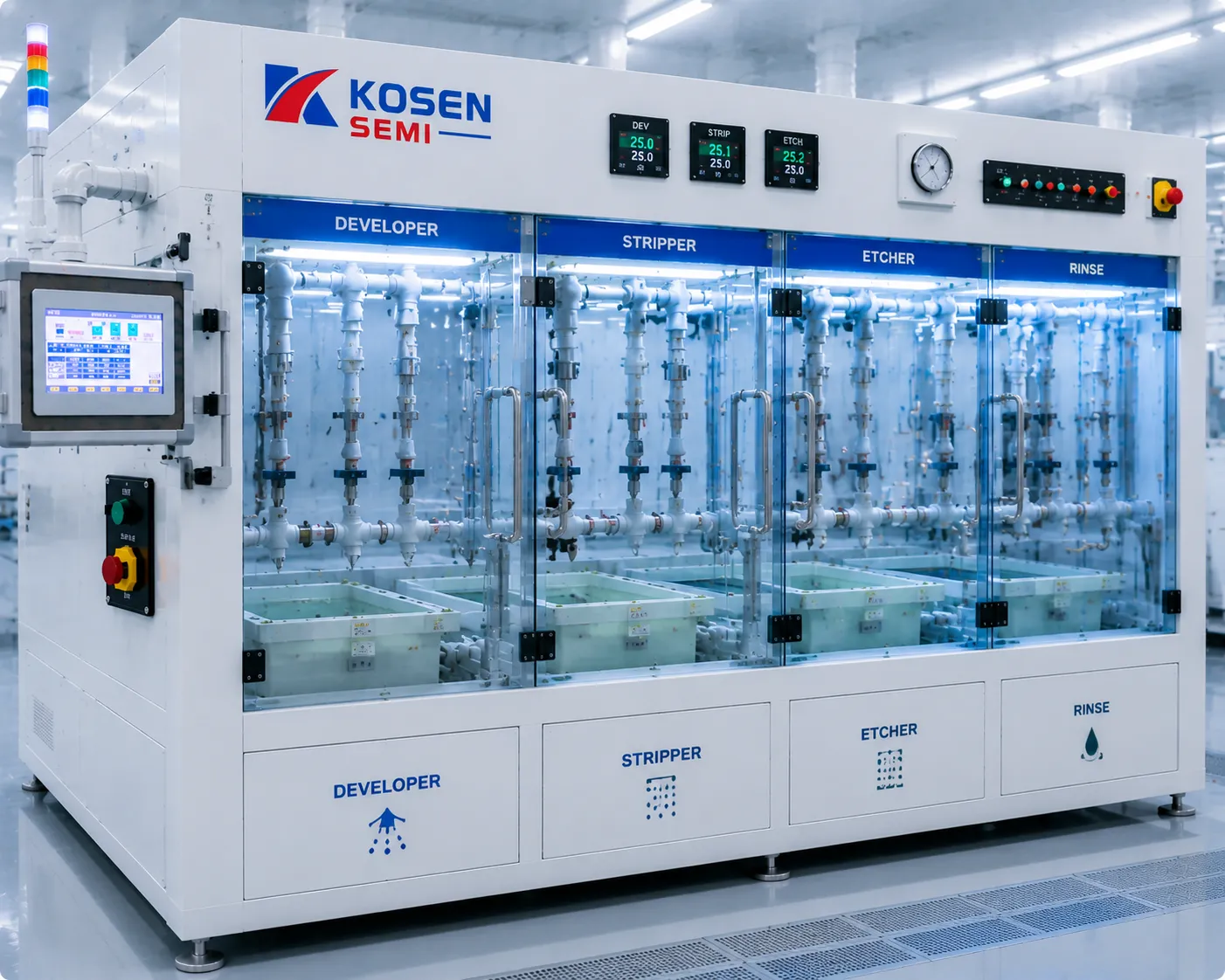
Integrated Wet Developer / Stripper / Etcher
A versatile multi-process platform combining photoresist stripping, high-uniformity wet chemical etching, and precise developing into a single enclosed optoelectronic wet processing equipment solution.
- Substrate Size
- 2–8 Inch Wafer
- Target Device
- Advanced Photonics
Core Parameters & Specification Comparison
Compare process capability, substrate scalability, and cleanroom ratings across KOSEN SEMI automated wafer cleaning systems and wet processing products.
| Equipment Model | Substrate Scale | Cleanroom Rating | Automation Level | Primary Process Application |
|---|---|---|---|---|
| Single-Wafer Optoelectronic Cleaner | 2–8 inch (50–200mm) | ISO Class 5–7 | Full-Auto | Low-Damage Single-Wafer Cleaning & Drying |
| Multi-Tank Batch Wet Bench Station | 2–8 inch (50–200mm) | ISO Class 5–7 | Semi / Full-Auto | High-Volume Substrate Cleaning & Wet Chemical Etch |
| Integrated Developer / Stripper / Etcher | 2–8 inch (50–200mm) | ISO Class 5–7 | Full-Auto | Multi-Step Resist Stripping, Etching, & Developing |
Scalable Fab Hardware from R&D to Production
KOSEN SEMI designs modular wet processing hardware tailored to your unique fab layout and chemical compatibility needs. Contact our applications team to configure custom tank layouts, robotic handling, and automated chemical delivery systems.
Yield-Focused Optoelectronic Processing and Cleanroom Integration
High-stakes photonic and compound semiconductor fabrication demands uncompromising cleanliness and operational reliability. KOSEN SEMI engineers optoelectronic wet processing equipment built strictly to eliminate commercial procurement risk and deliver measurable yield enhancement optoelectronics performance, leveraging our extensive Engineering Capability across the photonic industry.
Our automated wafer cleaning platforms are designed for integration into ISO Class 5–7 cleanroom environments. Equipment safety features and applicable project requirements can be reviewed during technical evaluation. By integrating automated chemical dosing, controlled fluid filtration and recirculation, and advanced drying technology, KOSEN SEMI empowers global optoelectronic manufacturers to lower defect density while sustaining maximum tool availability.
Recorded across 100+ active global optoelectronic production lines operating 24/7.
Full compliance with ISO 14644-1 ultraclean air and chemical containment requirements.
Proven yield enhancement optoelectronics metric in high-volume optical communications manufacturing.
Drastic reduction in surface particle levels at 200 nm, with optimized evaluation down to 100 nm.
Documented Cleanroom Integration & Equipment Safety
Configurable Risk Controls
Cleanroom compliance optoelectronics requires precise hardware architecture to prevent particle generation, volatile chemical cross-contamination, and static-induced substrate damage. Every KOSEN SEMI wet processing platform undergoes rigorous factory acceptance testing (FAT) to verify full alignment with international semiconductor manufacturing protocols.
- ✓ Localized ISO Class 5–7 Airflow & Enclosure Design Constructed with high-purity FM4910 plastic materials, dynamic laminar air management, and HEPA/ULPA filtration integration to help maintain controlled processing conditions around critical zones.
- ✓ SEMI S2 & SEMI S8 Safety Compliance Full compliance with environmental, health, safety, and ergonomic guidelines, featuring automated chemical interlocking systems and dual-containment fluid piping.
- ✓ CE Marking & Electrical Safety Protocols Safety and electrical configurations can be aligned with applicable project requirements for industrial control, high-voltage isolation, and electromagnetic compatibility (EMC).
Tier-1 Optical Communications Case Study
Proven Fab Performance
A leading global optical communications manufacturer faced yield bottlenecks during InP and GaAs laser diode manufacturing due to surface oxidation and microscopic residue on sub-micron structures. Transitioning to KOSEN SEMI Automatic Wet Bench Systems resolved critical contamination vectors.
By implementing megasonic physical cleaning and IPA Marangoni high-uniformity drying, the customer completely eliminated watermarks and micro-particulate surface defects, accelerating ramp-up speeds for high-speed laser diode arrays.
Cleanroom Integration & Equipment Configuration Overview
To support complex optoelectronic wet processing workflows, KOSEN SEMI integrates comprehensive safety, environmental, and cleanliness engineering into every system configuration. Discover our broad range of high-performance semiconductor-wet-bench-systems and review key architectural compliance parameters below:
| Compliance Area | Standard / Certification | Engineering Execution | Fab Impact |
|---|---|---|---|
| Particle Control | Designed for ISO Class 5–7 Environments | PFA fluid piping, sealed ambient chambers, real-time chemical filtration | Particle removal down to 100 nm under optimized conditions |
| Equipment Safety | SEMI S2 / SEMI S8 | Automated chemical leak detection, dual door interlocks, ergonomic loading heights | Zero operator chemical exposure risk |
| Fire Protection | FM4910 Standard | Flame-retardant PVDF and polypropylene body construction | Meets international semiconductor fab fire codes |
| Electrical & Directives | CE Marking / NFPA 79 | Redundant safety relays, industrial PLC control architecture, EMC shielding | Seamless integration with global power standards |
Trusted Across High-Growth Optoelectronic Sectors
Supporting semiconductor and photonics customers with configurable wet processing solutions
Documented Reliability: Every KOSEN SEMI wet process system is backed by comprehensive engineering support, factory testing documentation, and global on-site warranty service.
Optoelectronic Substrate Cleaning FAQ
Explore technical answers regarding optical device surface contamination control, compound semiconductor protection, substrate sizing flexibility, and pre-purchase process validation.
How do KOSEN SEMI systems prevent chemical corrosion on compound semiconductor surfaces like GaAs and InP?
Preventing unwanted oxidation and chemical corrosion on delicate III-V compound materials—such as Gallium Arsenide (GaAs) and Indium Phosphide (InP)—requires continuous atmospheric isolation. KOSEN SEMI wet processing systems utilize fully sealed process chambers featuring continuous high-purity Nitrogen purging to eliminate ambient oxygen exposure during critical wet chemical etching and advanced wafer cleaning systems operations.
Additionally, automated closed-loop chemical dosing systems maintain precise fluid temperature control within ±0.1°C alongside real-time concentration monitoring. High-velocity displacement rinsing immediately quenches active chemical reactions, preventing micro-pitting, surface staining, and optical haze across sensitive compound wafers.
- • Inert gas shielding isolates substrates from atmospheric oxygen during processing.
- • Precision chemical dosing maintains thermal stability within ±0.1°C to control etch rates.
- • Fast displacement rinsing halts chemical activity within milliseconds to prevent pitting.
What prevents fragile micro-structures or thin epitaxial layers from damaging during cleaning?
Fragile optoelectronic geometries—such as Micro-LED cantilevers, edge-emitting laser diode end-facets, and sub-micron epitaxial layers—are highly vulnerable to structural damage under conventional ultrasonic cavitation. KOSEN SEMI incorporates frequency-swept megasonic agitation operating between 0.8 MHz and 3.0 MHz within our Single Wafer Cleaning Systems to remove optical device surface contamination without generating destructive acoustic shocks.
By continuously modulating transducer frequencies, our wet stations eliminate localized standing-wave energy hotspots, ensuring uniform kinetic cleaning force across the substrate. Soft-start acoustic transducers and IPA Marangoni surface tension drying protect micro-features from hydraulic shear forces and watermark formation.
Removes particulate contamination down to 100 nm under optimized conditions without fracturing fragile optical micro-structures or peeling thin epitaxial films.
Are the wet processing systems capable of handling multi-size substrate transitions?
Yes. KOSEN SEMI wet processing systems accommodate high-mix manufacturing lines with modular tooling engineered for quick substrate transitions. Our platforms support 2-inch, 4-inch, 6-inch, and 8-inch wafers, as well as non-standard square optical substrates and thin carrier systems.
Transitioning between substrate dimensions requires minimal mechanical swap time, minimizing equipment downtime. Fully programmable PLC software dynamically adjusts fluid dispenses, spin speeds, megasonic energy levels, and nitrogen drying cycles to match specific wafer sizes and material fragility profiles.
How can we evaluate process compatibility before purchasing equipment?
We eliminate commercial and technical risks prior to capital investment through comprehensive pre-purchase process validation. Backed by our advanced Engineering Capability, our application process lab provides clients with preliminary cleaning tests and customized process tuning support using customer-supplied production wafers.
Fabs submit test substrates for baseline particle counts, Atomic Force Microscopy (AFM) surface roughness evaluation, and chemical residue inspection. KOSEN SEMI delivers detailed analytical reports documenting Particle Removal Efficiency (PRE), chemical consumption metrics, and optimized process parameters tailored to your exact fab requirements.
Consult Process Engineers
Connect directly with KOSEN SEMI wet process specialists to discuss custom chemical formulations, carrier tooling, or cleanroom integration needs.
Ready to Elevate Your Optoelectronic Yield?
Connect with KOSEN SEMI process engineers today to learn about our Engineering Capability. Request a complimentary sample cleaning test or receive a customized wet processing equipment proposal designed for your specific substrate requirements.