
Semiconductor Wet Process & Precision Cleaning Equipment
Engineered for high-yield wafer fabrication and advanced packaging, KOSEN SEMI delivers high-purity wet process architectures, automated wet benches, scrubber systems, and customized equipment solutions. Learn more about us and our engineering capabilities.
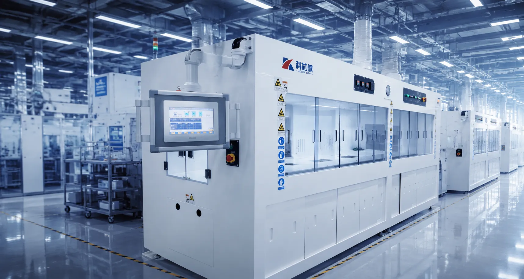
Advanced Wafer Cleaning Systems & Semiconductor Wet Bench Equipment
KOSEN SEMI delivers an integrated suite of high-purity wet process equipment engineered for semiconductor wafer fabs, compound semiconductor manufacturing, and advanced packaging facilities. From automated wet benches to specialized wafer cleaning systems and point-of-use scrubbers, our technology provides maximum uptime, precise chemical dosing, and superior yield protection.
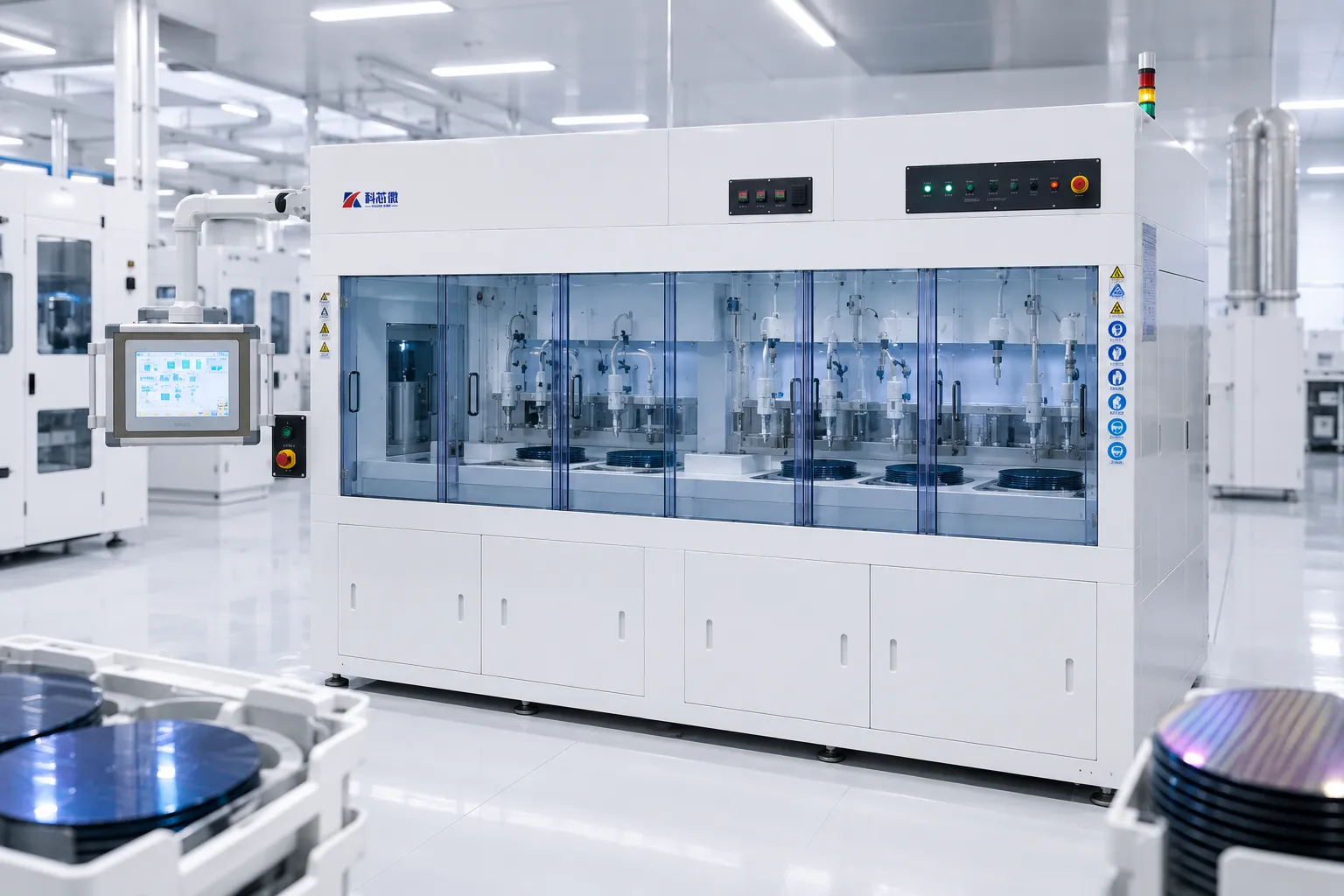 Single Wafer & Batch
 Wafer Cleaning Systems
Engineered for application-qualified particle removal at 200 nm, with optimized evaluation down to 100 nm, KOSEN SEMI wafer cleaning systems support versatile single wafer cleaning systems processing and high-throughput batch configurations. Integrated megasonic agitation and ultra-pure chemical dispensing ensure immaculate wafer surface conditioning.
- 99.9% Particle Removal Efficiency
- Single Wafer & Multi-Cassette Configurations
- ISO Class 5–7 Cleanroom Compatibility
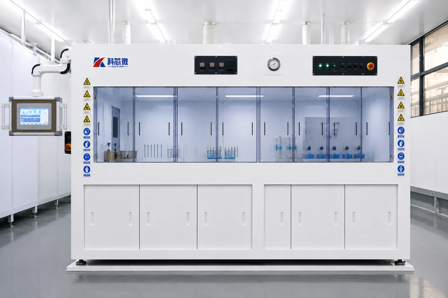 Automated & Manual
 Semiconductor Wet Bench Systems
Available in fully automated or manual operator configurations, our wet bench platforms offer precise temperature regulation and automated chemical dosing control. Ideal for RCA cleaning, SPM stripping, and wet etching across 150mm, 200mm, and 300mm substrate sizes.
- Precision Chemical Dosing & Thermal Control
- Robotic Transfer Arms & Sealed Enclosures
- Certified to SEMI S2 and SEMI S8 Standards
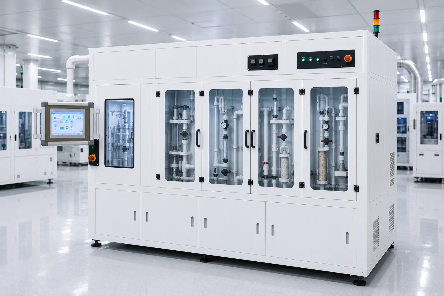 Point-of-Use Abatement
 Semiconductor Scrubber Systems
Industrial point-of-use wet scrubbers built for high-efficiency neutralization and abatement of toxic, acidic, and alkaline exhaust gases. Guarantees cleanroom environment safety and strict environmental emission compliance with automated pH balancing.
- High-Efficiency Acid/Alkaline Neutralization
- Real-Time Effluent & Gas Monitoring
- Low Utility & Water Consumption Architecture
 Ultra-Pure Processing
 Chemical Cleaning Equipment
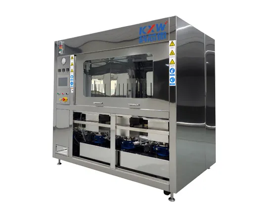
High-purity chemical blending cabinets and ultra-precision surface cleaning systems. Featuring automated chemical dosing, spiked concentration monitoring, and leak-proof fluoropolymer fluid paths to eliminate trace metal contamination.
- High-Purity PFA/PVDF Fluid Circuits
- Automated Chemical Dilution & Dosing
- Zero-Dead-Leg Valve Manifold Design
 OEM / ODM Custom Engineering
 Custom Semiconductor Equipment
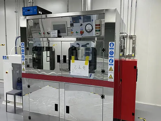
Engineering-grade OEM and ODM wet process solutions engineered for non-standard wafer sizes, specialized chemical recipes, and custom fab space constraints. Delivered with fast-track factory installation and complete validation testing.
- Computational Fluid Dynamics (CFD) Simulation
- Tailored Substrate Handling (SiC, GaN, MEMS)
- Modular Cleanroom Fabrication & Commissioning
Comprehensive Wet Process Hub
KOSEN SEMI provides end-to-end wet process equipment coverage. From single wafer cleaning and automated wet benches to point-of-use exhaust abatement, our team supports full facility integration and lifecycle optimization.
End-to-End Semiconductor Wet Process Solutions for Modern Wafer Fabs
In advanced semiconductor manufacturing, high-purity wet process steps are critical for maximizing yield and maintaining wafer surface integrity. As node architectures shrink and advanced packaging methods evolve, equipment managers and process engineers require reliable wafer cleaning systems and wet bench configurations that deliver rigorous particle removal efficiency without degrading fine substrate features.
KOSEN SEMI manufactures full-line semiconductor equipment designed to support every phase of fab wet processing. From precise single wafer surface preparation and automated wet benches to chemical distribution units and point-of-use scrubber systems, our tools are constructed using high-purity fluoropolymer fluid lines and zero-dead-leg valves to prevent contamination and optimize chemical consumption.
Custom Semiconductor Equipment & Tailored Wet Process Solutions
Advanced semiconductor manufacturing often requires specialized tool architectures that off-the-shelf platforms cannot accommodate. KOSEN SEMI serves as a trusted OEM and co-development engineering partner, supplying custom semiconductor equipment and tailored wet process solutions built specifically for non-standard wafer geometries, aggressive chemical formulations, and stringent cleanroom constraints. Learn more about-us and our core competencies. From multiphysics flow modeling to ISO Class 5–7 cleanroom integration, our engineering team works directly alongside fab process engineers to deliver high-yield, turn-key wet processing systems with maximum operational uptime.
Advanced Engineering & CFD Fluid Dynamics Modeling
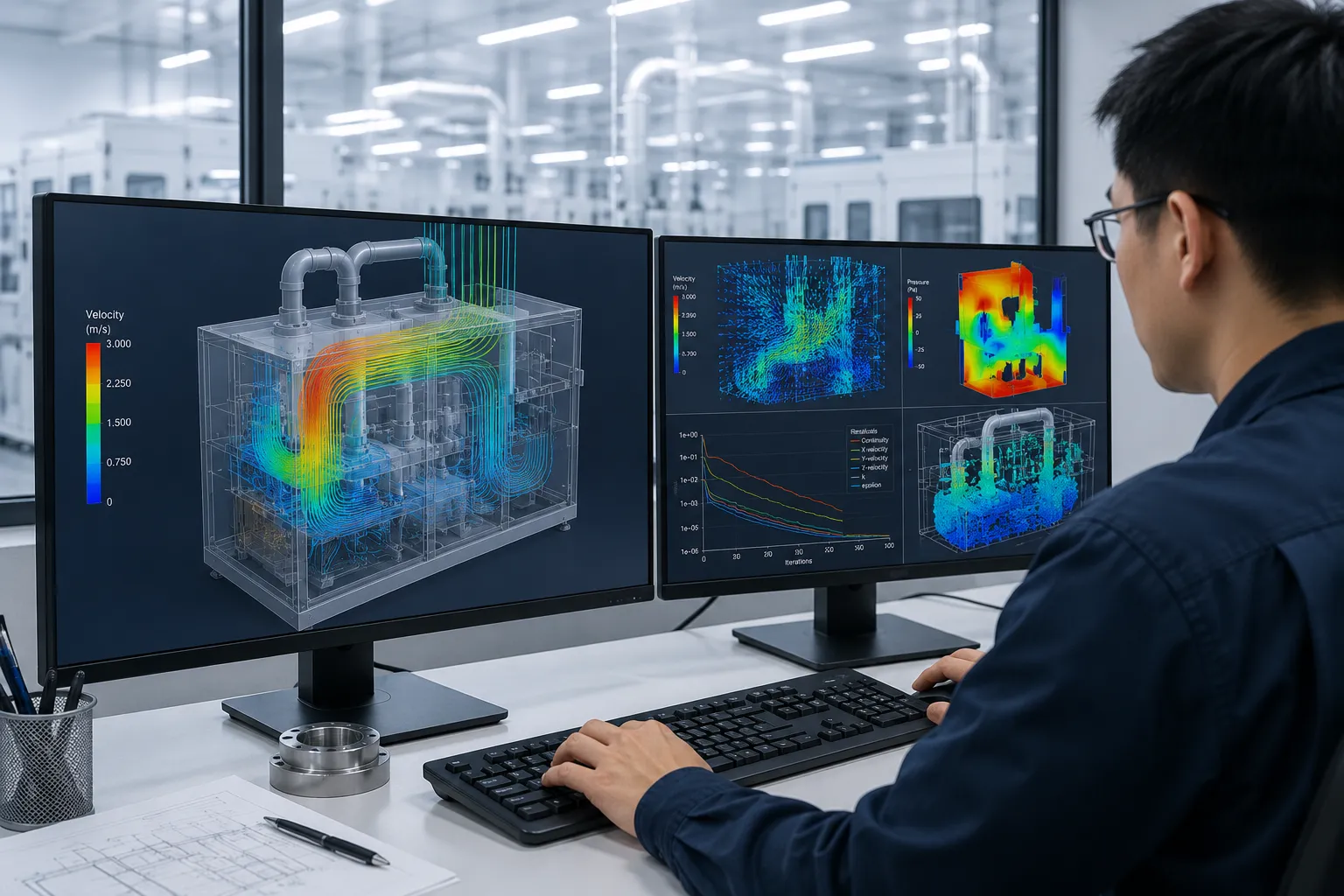
Every custom equipment build begins with rigorous digital prototyping and multi-domain simulation backed by our advanced Engineering Capability. KOSEN SEMI utilizes 3D CAD modeling paired with Computational Fluid Dynamics (CFD) chemical flow analysis to optimize fluid distribution, bath recirculation, and chemical agitation dynamics. This predictive modeling eliminates flow stagnation zones and minimizes boundary-layer turbulence, ensuring uniform chemical exposure across every square millimeter of the wafer surface.
Our control software team develops modular PLC and SCADA automation frameworks, empowering fab engineers with complete control over chemical dispense timing, temperature regulation, megasonic energy levels, and dynamic recipe sequencing with repeatable precision.
- Multiphysics CFD Modeling: Simulates fluid dynamics, chemical boundary layers, and thermal gradients prior to physical fabrication.
- Proprietary PLC Architecture: Fully customized automation control supporting SECS/GEM interface and real-time process telemetry.
- Finite Element Analysis (FEA): Evaluates thermal and mechanical stress limits to ensure structural integrity in harsh chemical environments.
High-Purity Materials & Non-Standard Substrate Customization
To handle aggressive wet chemistries—including hot hydrofluoric acid, SC-1/SC-2, piranha (SPM), and organic solvents—KOSEN SEMI constructs custom wet bench enclosures and process tanks using ultra-high-purity (UHP) fluoropolymers and thermoplastics. These materials are also extensively deployed in our advanced wafer-cleaning-systems. All wetted fluid circuits feature continuous PFA tubing, seamless PTFE/PVDF baths, and chemical-grade manifolds engineered to prevent metallic ion leaching and particle contamination.
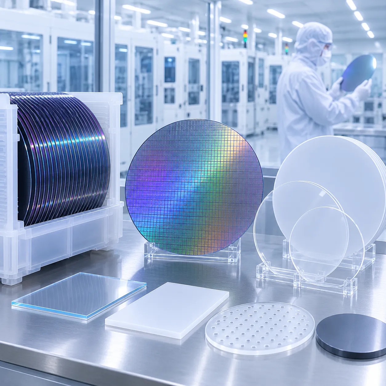
We specialize in custom robotic end-effectors, vacuum chucks, and specialized substrate carriers engineered for non-silicon materials, fragile thin wafers, and non-standard form factors such as Silicon Carbide (SiC), Gallium Nitride (GaN), Quartz, Glass, and Sapphire.
Corrosion-Resistant Polymers
Exclusive use of virgin PTFE, PFA, PVDF, and FM4910-compliant plastics to eliminate chemical degradation.
Custom Substrate Handling
Tailored end-effectors and carriers designed for SiC, GaN, Glass, Quartz, thin wafers, and square panels.
4-Stage Custom Engineering & OEM Delivery Process
Our structured four-stage engineering methodology ensures transparent project tracking, rigorous design validation, and rapid cleanroom commissioning for custom wet processing tools.
Requirement & Recipe Analysis
Comprehensive evaluation of chemical process recipes, etch rate targets, cleanliness metrics, and cleanroom footprint requirements.
Simulation & Mechanical Design
3D CAD modeling, CFD fluid flow optimization, structural FEA validation, and detailed sign-off on design specs.
Cleanroom Assembly & Wiring
Precision assembly, UHP orbital tube welding, and electrical integration executed inside certified ISO Class 5–7 cleanrooms.
FAT / SAT & On-Site Commissioning
Factory Acceptance Testing followed by seamless fab installation, Site Acceptance Testing, and process recipe fine-tuning.
Custom Engineering Capabilities & Technical Scope Matrix
KOSEN SEMI accommodates complex non-standard tool requirements across R&D pilot lines, compound semiconductor fabs, and high-volume 200mm/300mm manufacturing plants. Below is an overview of our custom design envelope:
| Engineering Domain | Standard Capabilities | Custom & OEM Scope |
|---|---|---|
| Substrate Compatibility | 150mm, 200mm, and 300mm standard circular silicon wafers | SiC, GaN, Glass, Quartz, Sapphire, square substrates, and ultra-thin wafers (<100 µm) |
| Wetted Construction Materials | High-purity PTFE, PFA, PVDF, and FM4910 fire-rated plastics | Custom quartz process tanks, conductive PFA, and titanium/quartz immersion heating loops |
| Automation & Robotics | Single-axis and multi-axis linear robotic wafer transfer systems | Multi-station overhead robotics, dual-arm custom end-effectors, and full SECS/GEM integration |
| Safety & Environmental Compliance | SEMI S2 / S8 certified, CE compliant, FM4910 fire protection ready | Double-containment fluid tubing, EMO loop integration, and localized dual-exhaust ventilation |
Submit Your Custom Design Specifications & CAD Files
Have a unique wet process requirement, specialized wafer substrate, or tight cleanroom layout? Upload your process flow diagrams, CAD models, or technical RFQ specifications directly to our senior equipment design team.
Wet Process Equipment Selection & Technical Specification Matrix
Evaluating semiconductor wet process equipment requires precise alignment between chemical dynamics, wafer throughput, and yield target requirements. Use the interactive technical matrix below to compare KOSEN SEMI tool configurations across substrate sizes, automation frameworks, cleanroom integration levels, and chemical compatibility specs. Built in accordance with international SEMI safety and operational standards, our systems ensure high-purity processing with optimized Total Cost of Ownership (TCO). Our engineering team maintains a sharp focus on continuous innovation and process perfection.
| Parameter | Wafer Cleaning Systems | Wet Bench Systems | Scrubber Systems | Chemical Cleaning Equipment | Custom Semiconductor Equipment |
|---|---|---|---|---|---|
| Compatible Wafer Sizes | 100mm, 150mm, 200mm, 300mm (4"–12") | 100mm, 150mm, 200mm, 300mm (4"–12") | N/A (Point-of-use exhaust abatement) | 100mm, 150mm, 200mm, 300mm (4"–12") | Custom formats, panels & substrates up to 300mm |
| Automation Level | Single Wafer Cleaning Systems / Inline Track / High-Capacity Batch | Fully Automated Robotic Arm / Semi-Auto / Manual | Fully Automated (Integrated PLC & SCADA) | Fully Automated Chemical Delivery & Recipe Control | Engineered to spec (Manual to autonomous cluster) |
| Process Node Compatibility | 200 nm production nodes; optimized capability down to 100 nm | 200 nm to mature process nodes; optimized capability down to 100 nm | Universal compatibility across all fab nodes | 200 nm to mature wafer fabrication; optimized capability down to 100 nm | Tailored per node specification & defectivity target |
| Cleanroom Class Requirement | ISO Class 5–7 | ISO Class 5–7 | Sub-fab / Utility room enclosure integration | ISO Class 5–7 | Configurable to client cleanroom footprint |
| Chemical Compatibility | Dilute HF, RCA (SC-1/SC-2), SPM, Megasonic DIW, O3 | HF, BOE, Hot Phosphoric, SPM, Solvents, RCA | Acidic fumes (HF, HCl), Alkaline exhaust (NH3), NOx | High-purity HF, H2O2, IPA, organic solvents | Broad chemical matrix including proprietary mixtures |
| Particle Removal Efficiency | 99.9% PRE at 200 nm, with optimized evaluation down to 100 nm | 99.5% PRE (application & bath setup dependent) | 99.9% scrubbing & neutralization efficiency | 99.7% surface defect removal rate | Engineered to custom target defect density metrics |
| Throughput | Up to 300 wph (Batch); 60–80 wph (Single-Wafer) | 50–200 wph (Batch size & recipe duration dependent) | Up to 3,000 m³/h continuous exhaust airflow rate | 60–150 wph continuous line throughput | Tailored to fab capacity targets & takt time |
| SEMI Standards Compliance | SEMI S2, S8, F47, E10 compliant | SEMI S2, S8, F47 safety certified | SEMI S2 compliant & CE certified | SEMI S2, S8, F57 fluid purity compliant | Full SEMI compliance suite tailored per region |
| Fluid Wetted Materials | PFA, PVDF, Natural Polypropylene, Quartz | PFA, PVDF, Quartz, PTFE, ECTFE | High-density PP, FRP, CPVC, PFA | High-purity PFA, PVDF, Quartz, Teflon | Process-specific high-purity polymer/quartz selection |
| Typical Applications | Pre-diffusion, post-CMP clean, post-etch residue removal | Wet etching, photoresist stripping, surface preparation | Fab acid/alkali exhaust neutralization & abatement | High-purity surface conditioning & chemical preparation | Compound semi (SiC/GaN), MEMS, advanced packaging TSV |
Choosing by Wafer Format & Size
All KOSEN SEMI wet process platforms accommodate 100mm to 300mm wafer formats. For 300mm high-volume manufacturing, specialized wafer cleaning systems and automated batch wet benches offer maximum particle removal and contamination control. For smaller 100mm–200mm lines or compound semiconductors (SiC/GaN), flexible carrier configurations optimize throughput without compromising process uniformity.
Choosing by Automation & Throughput
Fully automated robotic transfer systems minimize operator exposure, eliminate cross-contamination, and ensure consistent recipe timing across advanced nodes. Semi-automated and manual wet bench systems provide modular flexibility and cost-effective operation for R&D facilities, pilot lines, and specialized low-volume production.
Choosing by Chemical & Material Compatibility
Chemical selection dictates fluid path construction. Hydrofluoric acid (HF) and RCA chemistry require inert PFA or quartz components, while SPM (sulfuric peroxide) and organic solvent stripping demand chemical-resistant polymers engineered for thermal stability. KOSEN SEMI validates all fluid-wetted components prior to FAT/SAT delivery.
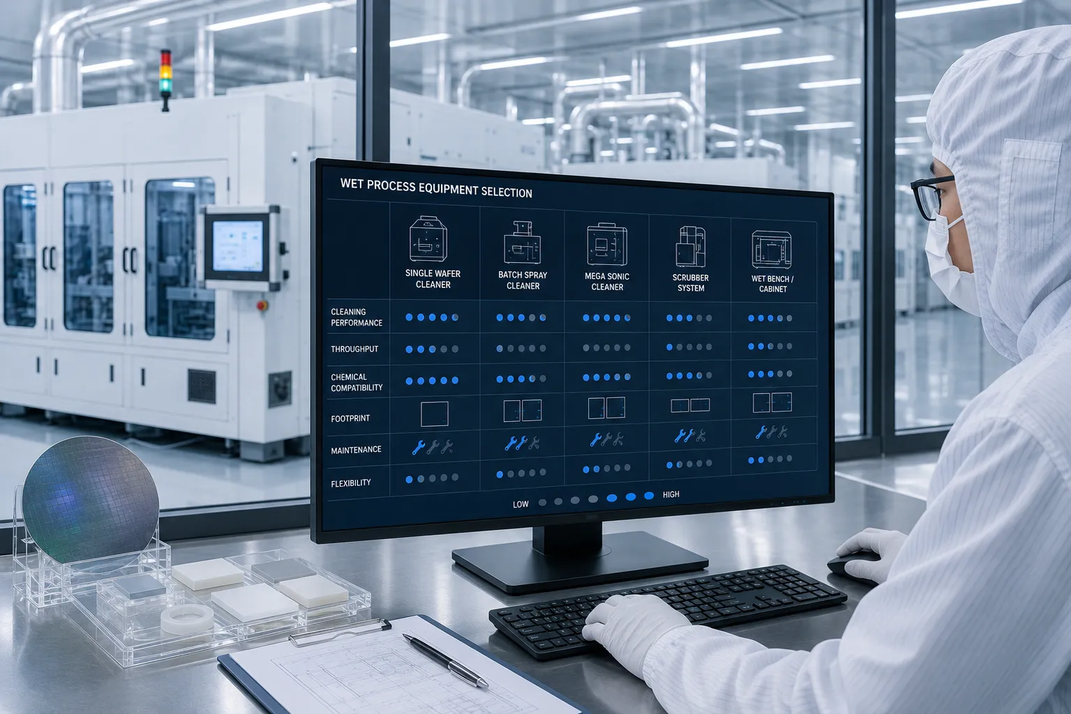
How to Evaluate Semiconductor Wet Process Equipment Specifications
Selecting semiconductor wet process equipment requires process engineers and fab facility directors to meticulously match tool performance with specific process node targets and defectivity tolerances. Key metrics such as Particle Removal Efficiency (PRE), chemical flow uniformity, megasonic power transfer, and thermal recovery times directly impact overall wafer yields. KOSEN SEMI engineers build every system with modular fluidics and high-precision chemical dosing loops, ensuring consistent micro-contamination control across both front-end-of-line (FEOL) and back-end-of-line (BEOL) applications.
Beyond process parameters, equipment safety and compliance remain primary considerations for modern semiconductor fabs. KOSEN SEMI systems adhere strictly to international SEMI standards, including SEMI S2 for environmental safety and health, SEMI S8 for ergonomics, and SEMI F47 for voltage sag immunity. By combining robust ultra-high purity wetted materials (PFA, PVDF, and quartz) with real-time PLC monitoring and automated fault diagnostics, our wet benches, wafer cleaning systems, and point-of-use scrubber equipment minimize unplanned downtime, delivering industry-leading reliability and low Total Cost of Ownership (TCO).
Industry Applications and Semiconductor Process Fit
KOSEN SEMI engineers high-purity wet process equipment precisely matched to demanding semiconductor manufacturing lines worldwide. From high-throughput front-end wafer fabrication to high-density advanced packaging wet process applications, our customizable wet benches, automated wafer cleaning systems, and specialized chemical processing tools optimize yield, ensure particle removal efficiency, and maintain reliable process repeatability across diverse substrate architectures. Supported by our advanced Engineering Capability, we deliver customized semiconductor manufacturing solutions worldwide.
Front-End Wafer Fabrication Equipment & Cleaning Solutions
Front-end wafer fabrication facilities demand uncompromising chemical purity and strict contamination control across 200 nm device nodes, with optimized capability down to 100 nm. KOSEN SEMI delivers robust wafer fabrication equipment engineered for critical cleaning, oxide stripping, and surface preparation. Our automated single-wafer and batch wet processing architectures optimize overall yield while ensuring complete chemical isolation and strict SEMI standard compliance.
- Silicon Wafer Cleaning: Advanced RCA clean and SPM/APM/HPM chemical sequences achieve particle removal efficiency (PRE) exceeding 99.9% for 200 nm-class contaminants, with optimized removal down to 100 nm without substrate loss.
- Native Oxide Removal: Precision dilute hydrofluoric acid (DHF) dispense and Megasonic-assisted agitation deliver highly uniform oxide etching and precise surface termination prior to epi-growth.
- Post-Etch Residue Cleaning: Formulated aqueous and solvent cleaning chemistries strip organic polymers, dry-etch residues, and photoresist films while safeguarding sensitive gate features.
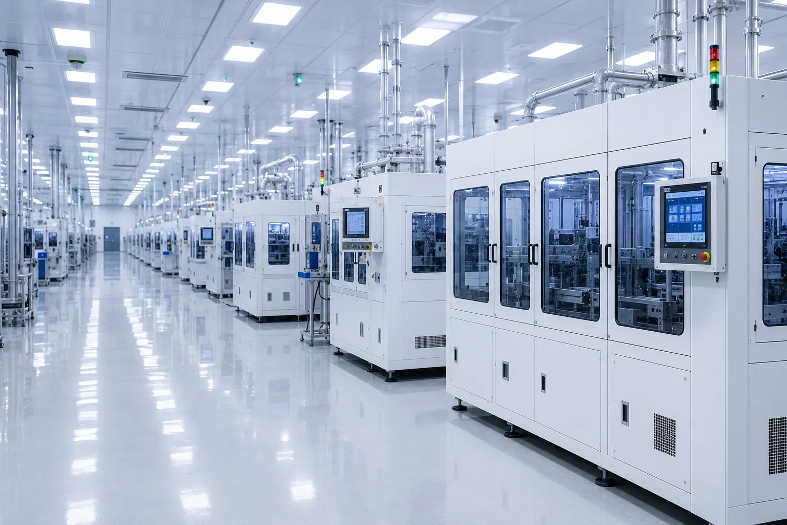
Single Wafer Cleaning Systems and Automated Wet Bench Systems configured for ISO Class 5–7 cleanrooms.
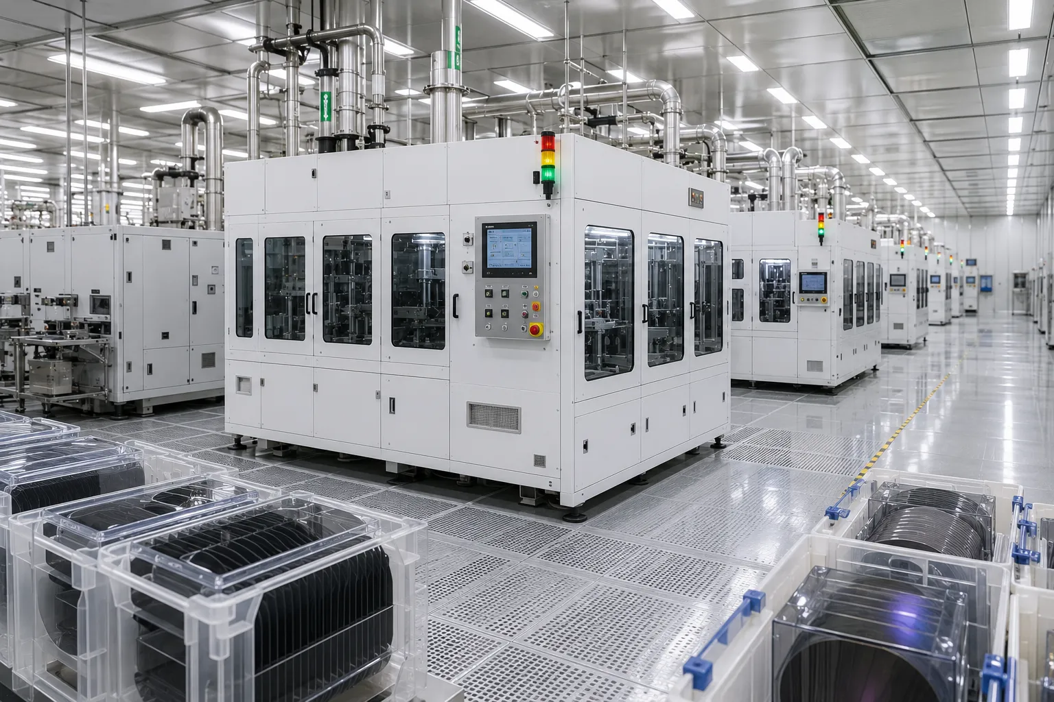
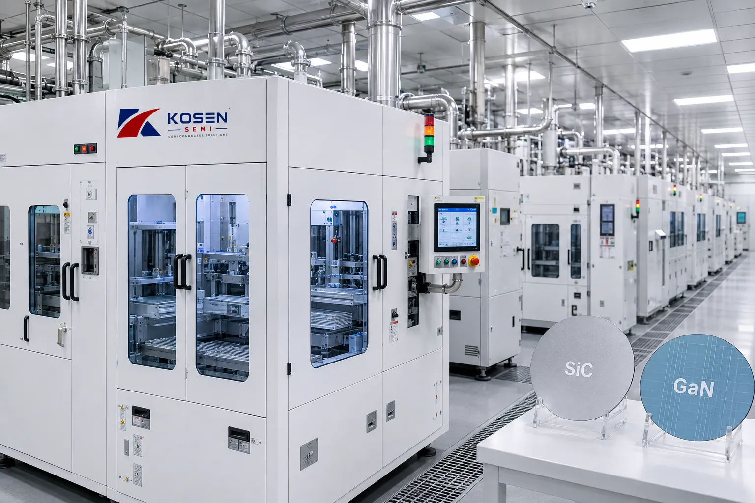
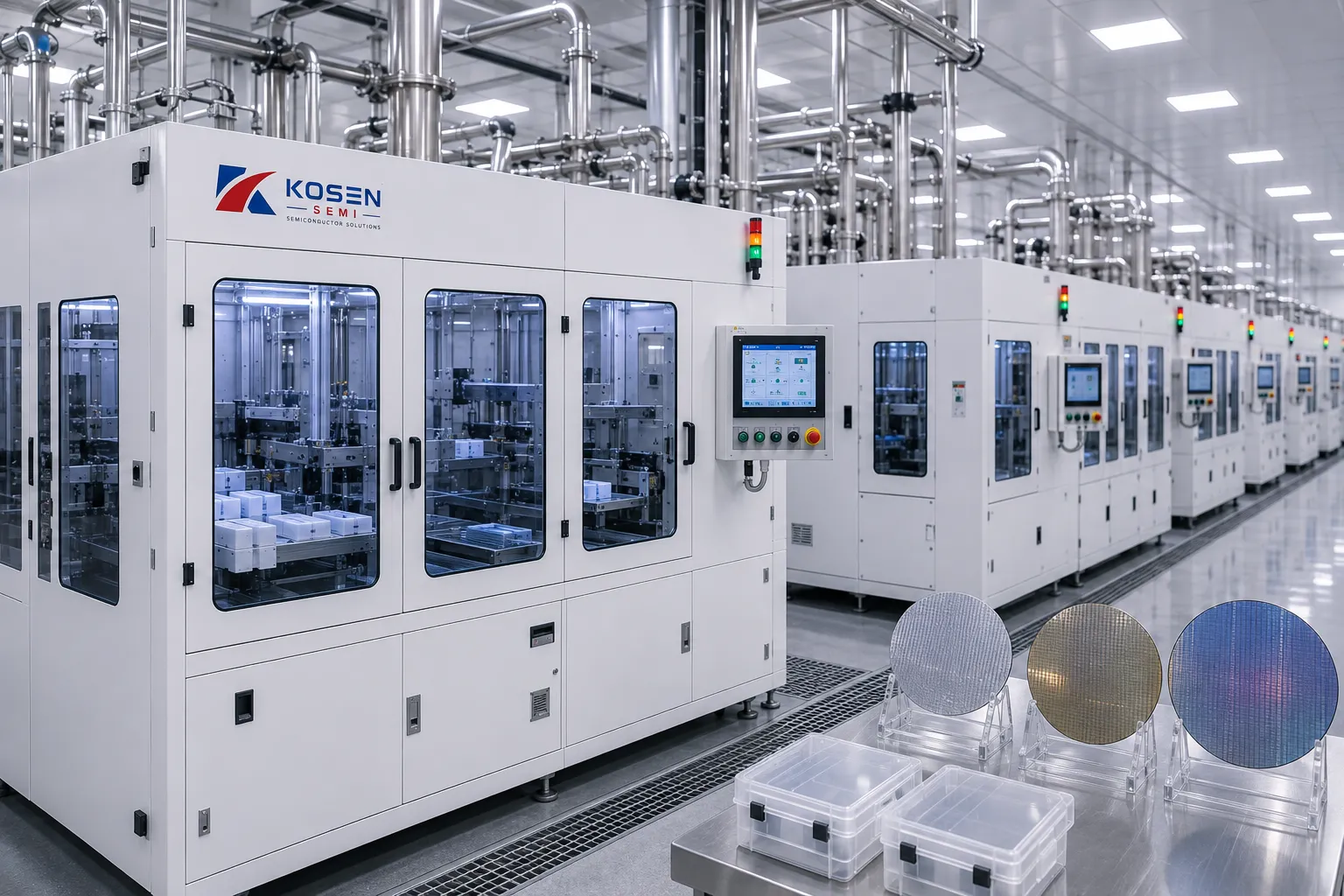
ISO Cleanroom Certified Semiconductor Equipment Manufacturer
As an ISO cleanroom certified semiconductor equipment manufacturer, KOSEN SEMI enforces rigorous quality assurance, ultra-clean assembly protocols, and SEMI-compliant engineering for risk-free fab integration. Learn more about-us and our commitment to cleanroom excellence.
ISO Class 5–7 Cleanroom
Precision wet processing components and fluid delivery systems are assembled within certified ISO Class 5–7 cleanrooms to prevent airborne contamination.
ISO Class 5–7 Facility
Main structural frame assembly and sub-system integration take place in dedicated ISO Class 5–7 cleanroom environments with continuous particle controls.
SEMI & ISO Compliant
Fully compliant with SEMI S2, SEMI S8, CE Directives, and ISO 9001:2015 standards, ensuring international EHS, ergonomic, and quality consistency.
Advanced Testing Protocols
100% helium mass spectrometer leak testing, automated software validation, and pre-shipment dry-run performance testing on all tools.
ISO Cleanroom Assembly Environment
All semiconductor wet process equipment manufacturing at KOSEN SEMI occurs inside certified ISO Class 5–7 cleanroom environments at our state-of-the-art manufacturing-facility. Strict particle management, positive-pressure air filtration, and continuous environmental monitoring prevent airborne contamination during critical assembly phases.
Our cleanroom facility supports the high-precision requirements of 200mm and 300mm wafer processing tools—including advanced Single Wafer Cleaning Systems—ensuring that high-purity PFA piping, chemical valves, and wafer-handling robotics meet pristine fab readiness prior to shipment.
Quality Assurance and Testing Protocols
To deliver long-term operational stability and yield reproducibility, KOSEN SEMI subjects every custom and standard wet processing tool to comprehensive factory verification:
- • 100% helium mass spectrometer leak testing for high-purity chemical manifolds and fluid delivery lines
- • Automated PLC control system validation, software interlock checks, and GUI functional testing
- • Pre-shipment dry-run testing to verify chemical dispense accuracy, flow rate stability, and thermal control
International Safety and Quality Certifications
As an experienced semiconductor equipment manufacturer, KOSEN SEMI maintains strict compliance with international EHS, ergonomic, and quality management standards:
SEMI S2 Standard
Environmental, Health, and Safety (EHS) compliance covering chemical containment, electrical safety, and emergency shutoff systems.
SEMI S8 Standard
Ergonomic design compliance optimizing operator safety, maintenance access, and human-machine interface usability.
CE Safety Directives
European Union machinery safety and electromagnetic compatibility (EMC) certification for global fab integration.
ISO 9001:2015 Certification
Quality Management System certification governing supply chain traceability, assembly procedures, and FAT acceptance.
These certifications reinforce KOSEN SEMI's commitment to zero-defect manufacturing standards, accelerating tool qualification (FAT/SAT) and reducing risk for global fab operators.
Buy Semiconductor Wet Equipment with Full Warranty and Clear Wet Bench Lead Time
Streamline tool procurement with predictable wet bench lead time schedules, robust global field services, and flexible warranty agreements tailored for modern semiconductor fabrication facilities through our complete range of semiconductor wet bench systems .
Rapid manufacturing cycles for standardized wet benches, automated stations, and exhaust scrubbers.
Tailored engineering, specialized substrate handling, and custom chemical delivery systems supported by our advanced Engineering Capability.
Immediate regional shipment of critical chemical pumps, valves, sensors, and robotics modules.
Comprehensive warranty coverage backed by dedicated local field application engineers.
Commercial Selection and Procurement Guide
What is the typical production lead time for standard vs. custom wet process equipment?
Standard semiconductor wet benches, Single Wafer Cleaning Systems, and exhaust scrubbers feature a predictable manufacturing wet bench lead time of 8 to 12 weeks. Fully customized automated multi-tank platforms range from 16 to 24 weeks, depending on component availability, specialized material routing (e.g., PTFE or PVDF), and engineering scope.
Accelerated manufacturing schedules and prioritized build slots are available for high-urgency cleanroom expansions and line upgrades.
Does KOSEN SEMI provide global on-site installation, commissioning, and training?
Yes. Our certified Field Application Engineers (FAEs) conduct rigorous Factory Acceptance Testing (FAT) prior to shipment, followed by on-site Site Acceptance Testing (SAT), facility hook-up oversight, and chemical process calibration.
We deliver comprehensive hands-on training for fab operators, process engineers, and maintenance staff across North America, Europe, and the Asia-Pacific region.
What safety standards and chemical containment certifications do your tools carry?
All wet processing systems are designed and certified to SEMI S2 (environmental, health, and safety) and SEMI S8 (ergonomics) standards. Enclosures incorporate double-containment fluid delivery tubing, Emergency Off (EMO) integration, automated chemical fire suppression interfaces, and continuous exhaust airflow monitoring.
Our tools also fully conform to CE Directives and ISO 9001 and ISO 14001 quality management guidelines.
How are spare parts, chemical pumps, and ongoing maintenance supported?
When you buy semiconductor wet equipment from KOSEN SEMI, you gain access to global spare parts hubs stocked with high-purity PTFE chemical pumps, valves, sensors, Megasonic transducers, and robotic handling arms for 24-to-48-hour dispatch.
Every equipment order includes a 12-to-24-month comprehensive warranty alongside optional Service Level Agreements (SLAs) and consignment inventory programs.
Streamlined Tool Integration and Commissioning
Integrating high-precision wet process platforms into fab environments requires precise synchronization between facilities engineering and tool manufacturers. KOSEN SEMI manages the procurement lifecycle from initial proposal to high-volume manufacturing ramp.
- ✓ Pre-install Utility Verification: Comprehensive Facility Requirement Documents (FRDs) provided early to align exhaust, chemical delivery, electrical, and DI water hookups.
- ✓ Factory Acceptance Testing: Thorough mechanical, safety, and process recipe validation inside ISO Class 5–7 cleanroom assembly bays prior to shipping.
- ✓ Site Acceptance Testing: Complete turn-key hookup verification, helium leak testing, and chemical calibration by dedicated field engineers.
Global Aftermarket and Maintenance Infrastructure
Unplanned equipment downtime directly impacts wafer yield and fab revenue. KOSEN SEMI operates an agile worldwide service network to maintain peak tool performance and maximize equipment operational lifespan.
- ✓ Consignment Inventory: Strategic stocking of critical pumps, valves, seals, and sensors at your fab facility for zero-delay repairs.
- ✓ Dedicated Field Support: Rapid-response field application engineers deployed locally for emergency troubleshooting and routine maintenance.
- ✓ System Retrofits: Modular hardware and control software upgrades to adapt installed wet benches to new substrate sizes or recipe requirements.
Ready to Optimize Your Semiconductor Wet Process Yields?
Connect with our process engineers today to receive detailed technical specifications, budget proposals, or custom tool evaluations. As a premier semiconductor equipment supplier, KOSEN SEMI delivers high-purity wet process architectures engineered for maximum uptime, stringent contamination control, and superior fab productivity.
24-Hour Response Guarantee
Direct technical routing to senior application specialists.
Tailored Tool Architecture
Custom chemical recipes, automation, and footprint designs backed by our advanced Engineering Capability.
Get Equipment Quote
Submit your RFP parameters for rapid technical review and commercial proposals.