
Building Benchmark Reliability Across Semiconductor Equipment History
Founded with a commitment to mitigating contamination risks in high-yield wafer fabrication, KOSEN SEMI has evolved into a premier global wet bench manufacturer. Our lineage traces back to intensive fluid dynamics R&D and ultra-clean chemical handling protocols. Today, we design and manufacture complete wet processing platforms that power advanced microelectronics production worldwide.
As semiconductor manufacturing advances across 200 nm-class nodes, with optimized capability down to 100 nm, wafer surface purity directly dictates chip yield and long-term device stability. Driven by precision and reliability, KOSEN SEMI continues to advance wafer cleaning systems technology for modern microelectronics. We integrate state-of-the-art cleanroom manufacturing with customized engineering capability expertise to deliver robust, zero-contamination wet benches, automated single wafer cleaning systems, and eco-friendly chemical scrubber platforms.
Our Vision and Core Mission
Empowering global wafer fabrication facilities through 200 nm-class process control, with optimized capability down to 100 nm, absolute particle control, and sustainable chemical recycling architectures.
- Yield Optimization: Advanced fluid dynamics and megasonic assistance engineered to minimize surface defectivity and particle redeposition.
- Risk Mitigation: Proven long-term operational uptime and chemical compatibility tested across high-volume fab environments.
- Custom Flexibility: Tailor-fit chemical bath geometries, automated dosing modules, and precision fluid delivery networks.
Cleanroom Assembly
Equipment is assembled inside ISO Class 5–7 controlled environments to preserve pristine chemical purity.
Global Quality Compliance
Fully certified under ISO 9001 quality management systems and compliant with CE semiconductor safety standards for global deployment.
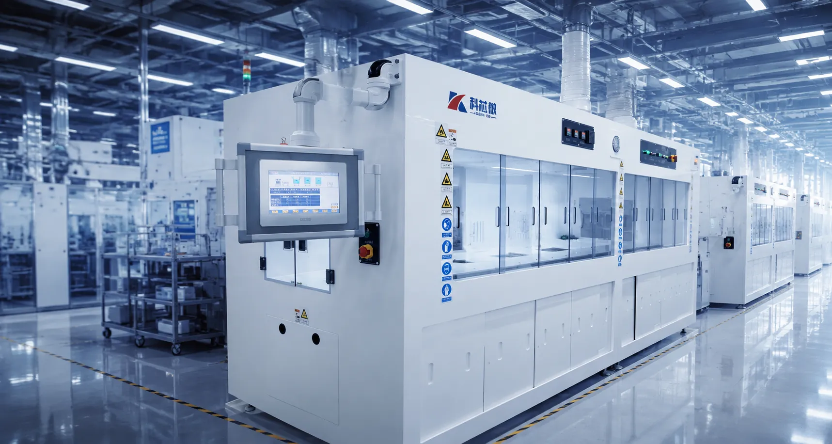
Mass production expansion of 300mm wafer wet benches and automated chemical scrubber platforms.
Company Foundation and Chemistry R&D
KOSEN SEMI established dedicated research initiatives focusing on microfluidic control and chemical flow architectures.
Automated Single-Wafer Platform
Successfully deployed our first fully automated single-wafer cleaning system into commercial fab lines, demonstrating proven field performance.
Ultra-Clean Facility and Quality Certifications
Commissioned a 10,000 m² cleanroom manufacturing facility base and secured international ISO 9001 quality system and CE compliance certifications.
300mm Wafer Wet Bench Platform
Expanded mass production of 300mm high-throughput automated wet benches and specialized chemical scrubber platforms for global wafer fabs.
The Core Pillars of Our Operational Excellence
KOSEN SEMI integrates a high-precision cleanroom manufacturing facility with customized semiconductor engineering capability to meet the stringent technical demands of modern semiconductor fabrication plants worldwide. Learn more about our engineering capability and commitment to quality.
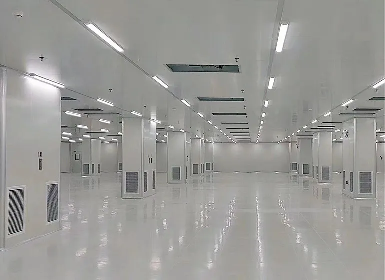
Cleanroom Manufacturing Facility
Scalable high-precision cleanroom manufacturing infrastructure engineered to deliver ultra-pure quality control and robust operational repeatability for demanding wafer cleaning systems and semiconductor processing equipment.
- 10,000 m² ISO Class 5–7 cleanroom manufacturing environment
- High-precision multi-axis CNC machining for tight component tolerances and fluid manifolds
- Automated ultra-pure assembly and integrated factory acceptance testing (FAT) lines
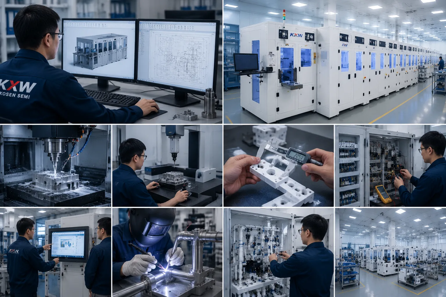
Custom Engineering Capabilities
Tailored semiconductor engineering capability designed to address complex chemical dynamics, advanced material compatibility, and proprietary automated control integration.
- Computational fluid dynamics (CFD) modeling for micro-level flow and chemical agitation analysis
- Advanced corrosion-resistant fluoropolymer (PFA/PTFE) materials selection and qualification
- Custom chemical bath geometries tailored to specific substrate sizes and process flows
- Seamless control software and SECS/GEM interface integration for automated fab operations
Rigorous Semiconductor Equipment Compliance and Quality Systems
KOSEN SEMI implements an uncompromising quality management system designed to maximize wafer yield, eradicate 200 nm-class particle contamination, and ensure continuous chemical delivery reliability. From stringent incoming material inspection to comprehensive Factory Acceptance Testing (FAT) and Site Acceptance Testing (SAT), our engineering procedures align with the world's most demanding microelectronics fabrication standards.
Every wet cleaning solution built by KOSEN SEMI undergoes rigorous testing to guarantee zero-contamination operation in critical cleanrooms. By integrating advanced quality protocols into every stage of development, we empower global semiconductor fabs with reliable, high-uptime wet bench and single-wafer cleaning systems processing equipment.
Ultra-Clean Assembly Protocols
Equipment assembly is executed within our certified manufacturing facility containing ISO Class 5–7 cleanrooms to eliminate airborne molecular contaminants and particle deposition.
- • Monitored particle controls calibrated down to thresholds aligned with 200 nm production and optimized 100 nm processes
- • High-efficiency ULPA filtration systems with positive-pressure airlocks
- • Mandatory full cleanroom garment protocol for all assembly technicians
High-Purity Fluoropolymer Materials
Exclusive deployment of virgin PFA and PTFE fluoropolymers prevents trace metal leaching and withstands aggressive chemical etching environments.
- • Virgin fluoropolymer chemical bath containment for ultra-pure fluid holding
- • Corrosion-proof fluid lines engineered for concentrated acid and solvent delivery
- • Trace metal extraction testing across all wetted chemical pathways
Precision Factory Inspection & Testing
Comprehensive quality controls guarantee total optical seal tightness, automated liquid metering, and strict particle count compliance.
- • 100% light-leakage inspections and full infrared weld seam integrity audits
- • In-line liquid particle counter validation across active chemical delivery lines
- • Automated flow rate calibration ensuring precise chemical dispensing
Global Certification & Compliance
ISO certification framework integrated alongside full CE mark safety and SEMI semiconductor equipment compliance standards.
- • ISO 9001 quality system certification covering design and manufacturing
- • CE compliance for electrical safety and electromagnetic compatibility
- • Strict alignment with SEMI S2 and SEMI S8 environmental and safety guidelines
End-to-End Lifecycle Quality Control Protocols
In modern semiconductor manufacturing, process repeatability and equipment reliability directly determine chip yield and fab profitability. KOSEN SEMI enforces a structured four-phase quality assurance framework across every wet bench, single-wafer cleaning system, and chemical scrubber unit. By controlling all manufacturing variables—from raw polymer selection to final fab commissioning—we deliver unmatched wafer cleaning quality and protect customer investments against unexpected process drift.
| Quality Phase | Inspection Focus | Verification Protocol | Quality Standard |
|---|---|---|---|
| Material Qualification | Virgin PFA, PTFE, and high-purity fluoropolymers | Spectrogram material analysis and chemical leaching resistance testing | Zero Contamination |
| Cleanroom Assembly | Chemical manifold welding and process bath construction | ISO Class 5–7 cleanroom assembly with infrared weld inspection | Full Weld Integrity |
| Factory Acceptance Testing | Full system fluidics, flow calibration, and particle counts | Liquid particle counting, light-leakage checks, and automated cycle runs | FAT Sign-Off |
| Site Acceptance Testing | Fab utility integration, chemical delivery, and safety interlocks | On-site process recipe verification and emergency shutoff validation | SEMI S2 Compliant |
Advanced Particle Control & Chemical Purity
Delivering consistent wafer cleaning quality requires precise fluid dynamic control and complete surface defect mitigation. KOSEN SEMI employs advanced liquid particle counters and laser scanners during factory validation. All chemical manifolds undergo automated high-purity DI water flushes to maintain trace ionic concentration levels well below stringent industry thresholds.
- Particle detection for 200 nm production, with optimized monitoring down to 100 nm
- Automated chemical concentration tracking and replenishment
- Corrosion-resistant seal integrity across high-temperature chemical baths
Global Safety Standards & Environmental Verification
Meeting international fab requirements demands full semiconductor equipment compliance. KOSEN SEMI equipment is backed by comprehensive engineering capability that ensures seamless integration into North American, European, and Asian fabs. From fail-safe interlocks to integrated chemical exhaust scrubbers, user safety and environmental compliance remain core engineering priorities.
- SEMI S2 environmental, health, and safety design compliance
- SEMI S8 ergonomic engineering for safe operator interaction
- Certified ISO certification quality management standards
International Standards & Compliance Credentials
Our manufacturing infrastructure and wet process equipment maintain active certifications validated by leading international auditing organizations.
ISO 9001 Standard
Quality System Management
CE Mark Compliance
European Industrial Safety
SEMI S2 Safety Protocol
Environmental Health & Safety
SEMI S8 Ergonomic Standard
Human Factors & Ergonomic Safety
Semiconductor Equipment Experts Driving Precision Wet Bench Solutions
The expert R&D team at KOSEN SEMI delivers tailormade wet bench engineering to fulfill complex process applications. Combining deep microfluidic science, advanced mechanical automation, and rigorous cleanroom chemical testing, our engineering subject matter experts accelerate yield optimization for semiconductor fabrication facilities worldwide.
Advanced Wet Process Engineering Brain Trust
Engineered for controlled particle levels and stable etching uniformity for 200 nm production, with optimized capability down to 100 nm, our specialized R&D division bridges fundamental physical research with high-volume manufacturing requirements. KOSEN SEMI maintains continuous innovation in computational fluid dynamics, ultra-pure chemical distribution, and megasonic energy transmission built around our world-class manufacturing-facility to ensure total customer trust.
- 20+ Senior Semiconductor Equipment Engineers Multidisciplinary specialists in chemical engineering, mechanical design, microfluidics, and automation controls.
- Patented Chemical Bath & Megasonic Drying Tech Proprietary chamber geometries and non-contact IPA vapor drying systems designed to eliminate wafer pattern collapse.
- 24/7 Global Remote & On-Site Process Tuning Dedicated field application engineers providing continuous equipment qualification, recipe optimization, and testing support.
"Every process chamber designed by our engineering team reflects over fifteen years of empirical validation, ensuring maximum fab throughput and flawless defect reduction."
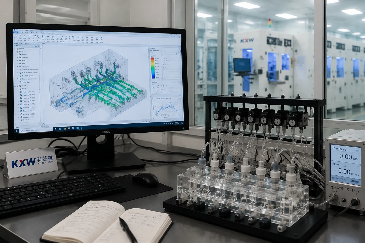
Utilizing 3D fluid modeling to simulate laminar chemical flows and thermal equilibrium across 200mm and 300mm wafer surface topographies.
Wet Process & Surface Chemistry Specialists
Our wet process research group focuses on optimized boundary layer reduction, targeted contaminant removal, and high-selectivity chemical etching. Working directly with fab yield managers, these semiconductor equipment experts refine dynamic chemical concentration management, temperature control algorithms, and ultra-pure DI water rinsing workflows. Learn more about our overall Engineering Capability.
Precision Tooling & Materials Engineering
Specializing in high-purity fluoropolymer fabrication and structural stress mitigation, this mechanical engineering team designs custom bath chambers and robust robotic wafer handling arms. Their mechanical architecture minimizes vibration and prevents micro-particle generation inside ultra-clean cleanroom environments.
SECS/GEM & Automated Control Engineers
Our automation software team builds intuitive human-machine interfaces and SECS/GEM compliant control systems for seamless MES integration. Providing precise real-time monitoring of fluid flow rates, temperature profiles, and multi-axis transfer kinematics, our controls ensure repeatable batch execution and complete process traceability.
Engage directly with our R&D engineering team for process feasibility studies, bath geometry customization, or custom control recipe design.