
Precision Metrics Driving Process Yield
KOSEN SEMI enforces strict engineering benchmarks across design, assembly, and thermal management—ensuring every wet process system delivers micron-level precision and uncompromising process control. Learn more about-us and our dedication to performance.
Thermal Control Precision
Sub-degree chemical temperature stability engineered to guarantee consistent etch rates and process repeatability.
Proprietary CFD Fluid Design
In-house Computational Fluid Dynamics modeling eliminates dead zones and optimizes chemical recirculation efficiency.
Cleanroom Assembly Standard
ISO Class 5–7 cleanroom environments prevent particulate contamination at our manufacturing-facility during system fabrication.
Custom Systems Deployed
Over 100 tailored wet bench and advanced wafer-cleaning-systems successfully delivered to global semiconductor manufacturers.
Quality Assurance Embedded Across Every Process Stage
From CFD flow field simulations to high-purity piping design and ISO-certified cleanroom assembly, KOSEN SEMI integrates total process validation into every custom equipment build.
Custom Equipment Engineering Across Semiconductor Applications
Different semiconductor sectors demand distinct chemical, thermal, and mechanical handling strategies. The KOSEN SEMI engineering team deeply understands specialized process characteristics across various sectors, engineering dedicated wet process equipment tailored to complex manufacturing requirements. From high-density interconnect micro-via cleaning in advanced packaging wet process workflows to aggressive compound power semiconductor cleaning and delicate MEMS wet process drying, our custom equipment engineering guarantees process repeatability, substrate protection, and continuous operational efficiency.
Advanced Packaging and High-Density Interconnect Cleaning
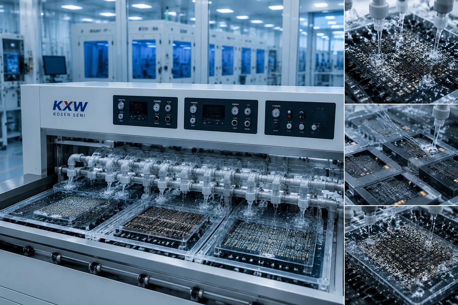
Modern 2.5D and 3D advanced packaging architectures demand immaculate micro-via residue removal and feature surface conditioning. KOSEN SEMI engineers specialized wet bench wafer cleaning systems that incorporate targeted megasonic and ultrasonic transducers to agitate fluid layers at high frequencies without compromising fragile wafer interconnect structures.
By optimizing chemical concentration delivery and fluid recirculation patterns, our advanced packaging wet process machinery removes particles at 200 nm production scale, with optimized removal down to 100 nm from deep aspect ratio blind vias while maintaining high throughput and minimal bath degradation.
Core Engineering Capability Highlights
- Frequency-Swept Megasonic Systems: Prevents standing wave damage while removing 200 nm-class contaminants, with optimized capability down to 100 nm from high-density vias.
- Boundary Layer Displacement: CFD-optimized chemical flow patterns ensure uniform exposure across entire wafer surfaces.
- Multi-Chemical Recirculation: Inline filtration down to 0.05 μm preserves chemical purity and extends bath operational life.
- Secure Automated Handling: High-precision robotic end-effectors ensure zero mechanical defect generation during transfer.
Quality Standards, Cleanroom Assembly, and Testing Validation
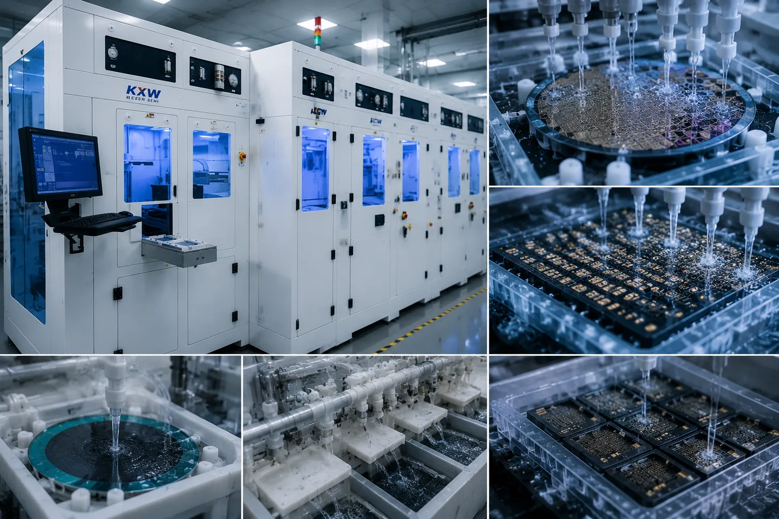
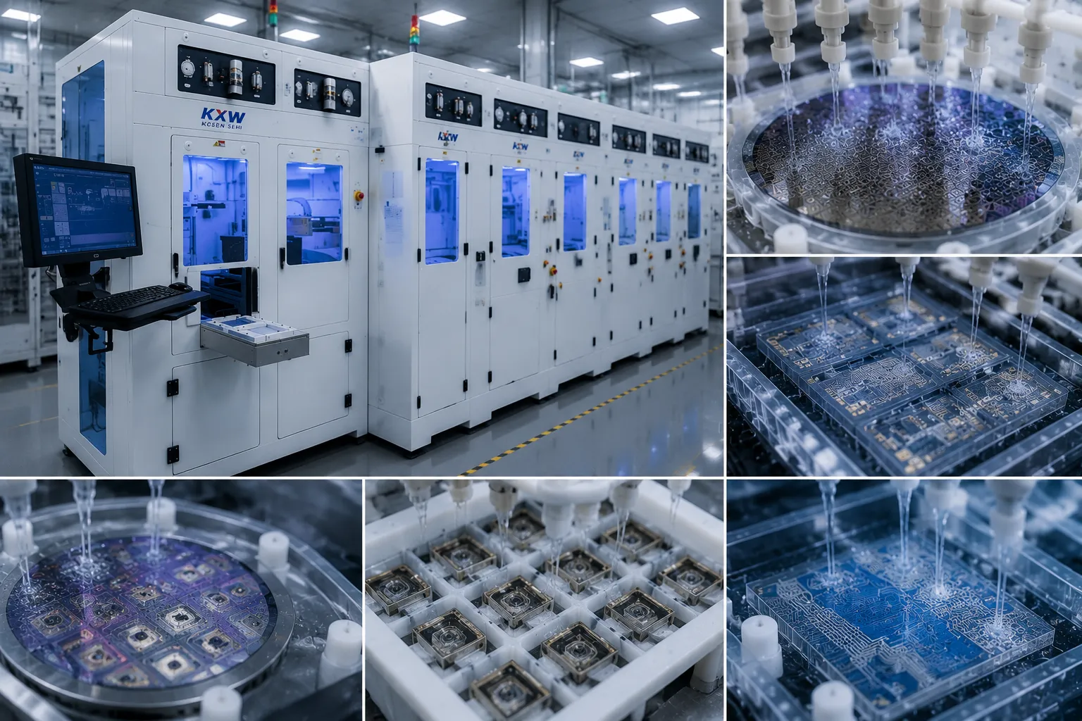
KOSEN SEMI strictly executes SEMI standards and comprehensive quality management systems across every phase of equipment manufacturing. From high-purity component machining to final ultrapure chemical testing, our facilities guarantee zero contamination, exceptional process stability, and full semiconductor equipment compliance for advanced fab operations.
Controlled Cleanroom Assembly Environment
Delivering high-yield wet processing solutions demands uncompromising environmental purity during tool construction. KOSEN SEMI operates dedicated ISO Class 5–7 cleanroom assembly zones engineered specifically for advanced wafer cleaning systems, including specialized Single Wafer Cleaning Systems, wet benches, and automated acid stripping machinery.
Our specialized technicians enforce strict cleanroom protocols during chemical fluid manifold integration and structural chassis assembly. High-purity fluoropolymer piping, including PFA, PVDF, and PTFE fluid lines, is welded and fitted inside ultra-filtered air environments to prevent ambient particulates and trace metallic ions from compromising internal fluid pathways.
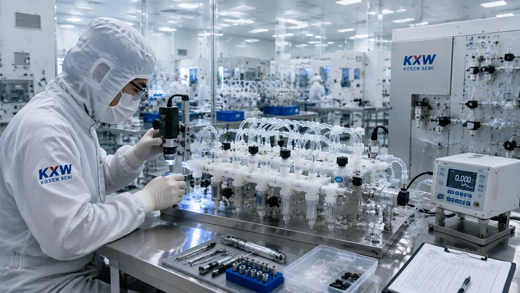
Ultra-clean chemical delivery manifold inspection inside KOSEN SEMI ISO Class 5–7 cleanroom assembly zone
International Safety & Compliance Certifications
Full compliance with SEMI S2 (Environmental, Health, and Safety) and SEMI S8 (Ergonomics) guidelines for seamless semiconductor fab integration.
Strict alignment with European Union Machinery Directives, Electromagnetic Compatibility (EMC), and Low Voltage Safety standards.
Certified quality management framework governing semiconductor wet bench systems engineering design, procurement, cleanroom assembly, and testing validation.
Precision Testing & Quality Validation Methods
Prior to tool dispatch, every custom engineering build undergoes rigorous physical, electrical, and chemical validation to ensure ultimate reliability and immediate factory acceptance.
- Helium Mass Spectrometer Leak Detection Ultra-sensitive vacuum and pressure decay testing to confirm zero-leak seal integrity across chemical, gas, and vacuum lines.
- Particle Counter Testing In-line liquid and airborne particulate monitoring for 200 nm production, with optimized monitoring down to 100 nm during dry operation and UPW recirculation cycling.
- Infrared Tube Welding Inspection Non-destructive thermographic examination of PFA and PVDF tube welds to guarantee completely smooth, bead-free interior surfaces.
Factory Acceptance Testing (FAT) & Safety Interlock Protocols
KOSEN SEMI executes structured verification protocols across all custom equipment builds. Our comprehensive Factory Acceptance Testing (FAT) and Site Acceptance Testing (SAT) frameworks guarantee full chemical containment, leak-free performance, and rapid automation interlock response prior to production line deployment.
| Validation Area | Inspection Method | Target Technical Benchmark | Quality Deliverable |
|---|---|---|---|
| Airtightness & Containment | Helium mass spectrometer leak testing under positive and negative differential pressure | < 1 × 10⁻⁹ mbar·l/s leak rate threshold | Certified mass spec leak inspection report |
| Fluoropolymer Weld Quality | Non-destructive infrared tube welding inspection and surface bead profile scanning | 100% bead-free continuous interior bore | Thermographic joint integrity & weld dossier |
| Process Water Cleanliness | Laser liquid particle counter (LPC) monitoring in UPW recirculation loops | Controlled particle level at ≥200 nm, per agreed process specification | Liquid particle baseline validation log |
| Electrical & Emergency Interlocks | SEMI S2 hazard sensor triggering and EMO push-button fault injection simulations | < 100 ms automated shutoff response | Third-party SEMI S2 compliance certificate |
Semiconductor Custom Engineering FAQ & Wet Process OEM Design
KOSEN SEMI delivers high-precision custom semiconductor equipment engineering and wet process OEM design solutions for demanding fab applications. Learn more about-us and explore technical insights below regarding custom wet bench engineering, development lead times, legacy system retrofits, and cleanroom manufacturing standards.
Yes, KOSEN SEMI specializes in complete end-to-end custom semiconductor equipment engineering. We design and build bespoke chemical wafer-cleaning-systems, spin rinser dryers (SRD), and automated wet benches tailored to client-specific process chemistries, unique fab layouts, and non-standard substrate dimensions (including Si, SiC, GaN, GaAs, and glass).
Our multidisciplinary engineering team integrates advanced thermal, chemical, and fluid mechanical design capabilities:
- Custom Flow Field Engineering: Self-developed CFD fluid dynamics simulations eliminate stagnant boundary layers and maximize chemical delivery uniformity across micro-structures.
- Tailored Tank & Cabinet Mechanics: Precision CNC machining of ultra-high-purity fluoropolymers (PFA, PVDF, PTFE) to withstand aggressive acid etching, solvent stripping, and high-temperature baths.
- Specialized Substrate Handling: Custom-engineered robot end-effectors, Bernoulli wands, and non-contact transfer mechanisms designed specifically for ultra-thin or fragile wafers.
- Bespoke Automation & Fab Integration: Seamless PLC architecture programming with SECS/GEM (E30/E37) host communications for fully automated fab line synchronization.
Custom wet process equipment delivery timelines typically range from 12 to 20 weeks from initial functional specification sign-off to Factory Acceptance Testing (FAT). Timelines vary based on tool complexity, chemical delivery automation requirements, and special component lead times.
KOSEN SEMI enforces rigorous milestone tracking across five structured engineering phases:
- Requirements & Process Alignment (Weeks 1–2): Analyzing chemical compatibility, bath turnover rates, target throughput (WPH), and facility footprint layout.
- 3D Mechanical & CFD Simulation (Weeks 3–6): izing 3D CAD models, structural FEA, chemical flow modeling, and safety interlock architectures.
- Cleanroom Component Machining & Assembly (Weeks 7–12): Precision CNC fabrication of chemical tanks, cabinet framing, and ISO Class 5–7 cleanroom mechanical assembly at our specialized manufacturing-facility.
- Software Programming & Electrical Integration (Weeks 13–15): Developing PLC logic, recipe management GUIs, safety sensor interlocks, and SECS/GEM interface protocols.
- Wet Process Testing & Validation (Weeks 16–18): Conducting chemical temperature stability tests, fluid flow verification, particle counts, and final FAT sign-off.
Yes, KOSEN SEMI offers specialized wet process OEM design modification and retrofitting services for legacy semiconductor manufacturing tools. Our engineering team evaluates existing equipment to modernize control systems, enhance process yields, and lower overall cost of ownership (COO).
Core wet bench retrofitting capabilities include:
- Control & Automation Modernization: Replacing obsolete hardware with modern PLC controllers, high-resolution touchscreen HMIs, and SECS/GEM smart factory interfaces.
- Chemical Loop & Piping Overhauls: Re-piping fluid delivery channels with high-purity PFA manifolds, advanced inline heaters, and precision temperature controllers (±0.1°C accuracy).
- Safety & Environmental Compliance: Upgrading chemical cabinet exhaust structures, fire suppression systems, emergency off (EMO) loops, and SEMI S2/S8 safety features.
- Process Chamber & Tank Conversions: Re-engineering process baths and quartz tanks to support larger wafer diameters, megasonic agitations, or advanced photoresist stripping.
Contamination control and chemical compatibility are paramount in semiconductor equipment engineering. KOSEN SEMI enforces stringent quality control procedures across raw material selection, machining, tube joining, and cleanroom assembly.
Our engineering quality assurance protocols feature:
- High-Purity Polymer Selection: Sourcing certified semi-finished PFA, PVDF, and static-dissipative PTFE polymers with complete lot traceability for aggressive acid and solvent resistance.
- ISO Class 5–7 Cleanroom Assembly: Assembling all chemical contact components, valves, and piping in certified cleanroom environments to eliminate airborne micro-particulates.
- Infrared (IR) Contactless Pipe Welding: Utilizing automated IR welding technology to guarantee seamless tube joins with zero internal bead projection or chemical trap sites.
- Helium Leak & Particle Inspection: Conducting high-vacuum helium mass spectrometer leak testing and DI water particle counting before tool shipment.
- Global Regulatory Compliance: Full certification adherence to SEMI S2 (Safety), SEMI S8 (Ergonomics), CE directives, and ISO 9001 quality management systems.
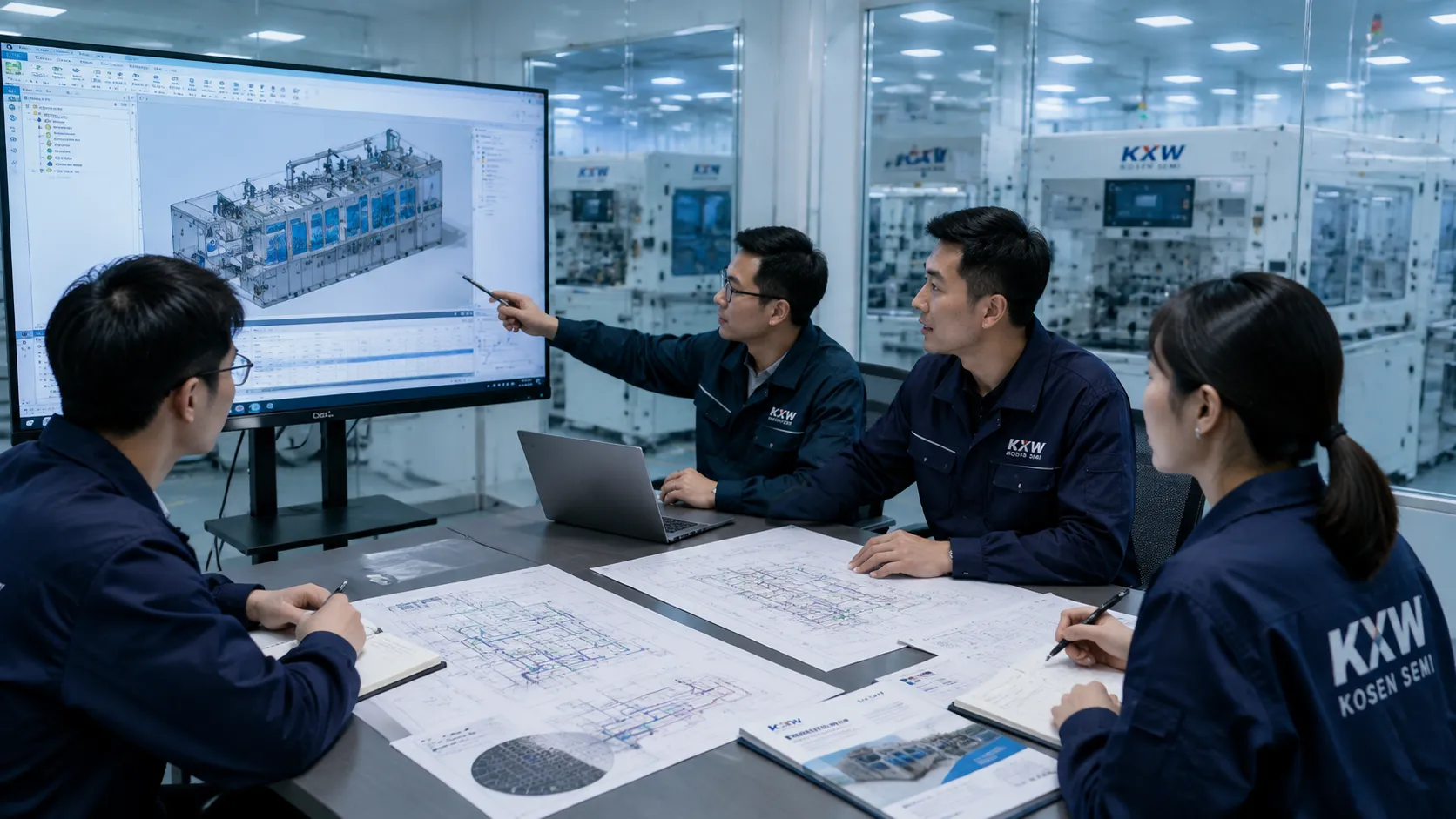
Direct Technical Consultation With KOSEN SEMI
Need customized technical solutions for your semiconductor wet process project? KOSEN SEMI engineering experts are available to discuss process optimization, fluid simulation, and custom equipment specifications.
Speak directly with experienced wet process equipment engineers.
Ready to Start Your Custom Semiconductor Wet Process Equipment Project?
Consult about-us at KOSEN SEMI today to receive a complimentary fluid simulation evaluation and a tailored custom wet process solution proposal for your fab line.
Speak directly with KOSEN SEMI engineering specialists to co-develop high-precision Automatic Wet Bench Systems and cost-effective semiconductor equipment solutions.
- Complimentary CFD Flow Evaluation: Validate bath velocity and chemical distribution prior to equipment fabrication.
- Tailored Hardware Engineering: Customized wet bench architectures using specialized Manual Wet Bench Systems, chemical delivery systems, and wafer cleaning modules.
- Rapid Engineering Consultation: Preliminary technical assessments and feasibility scoping delivered within 24 business hours.
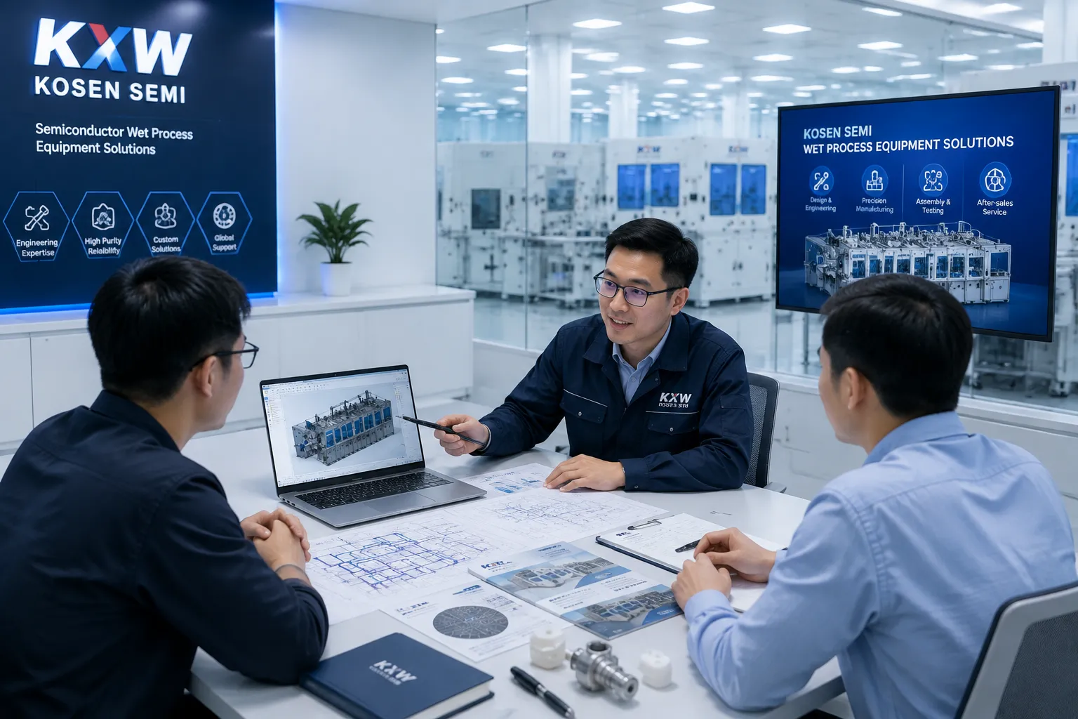
Request a Custom Wet Process Solution Proposal
Submit your project parameters below for immediate review by our engineering team.