
Quantifiable Yield Metrics & Global Compliance Standards
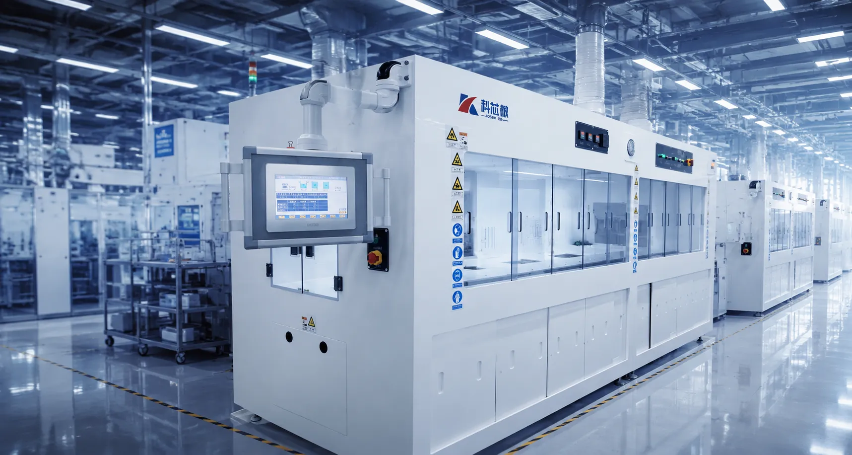
KOSEN SEMI delivers high-purity wafer cleaning systems engineered for yield enhancement, backed by SEMI S2/S8 standards, ISO certifications, and continuous fab operational auditing.
Targeting particles at 200 nm standard capability, optimized down to 100 nm to maximize semiconductor device yields.
Ultra-high-purity fluid handling with fluoropolymer components for minimized trace contamination risk.
Fab-proven wet bench and single-wafer scrubber availability for 24/7 continuous production.
Strict adherence to global safety, ergonomics, and cleanroom environmental standards.
 ISO 9001:2015 Quality Management SEMI S2 Safety Compliance SEMI S8 Ergonomics Standard CE Certified European Compliance ISO 14001 Environmental Safety RoHS / REACH Chemical Compliance
 Advanced Wafer Cleaning Systems Portfolio
Engineered for high-yield semiconductor fabrication, KOSEN SEMI provides state-of-the-art wet processing equipment. From Single Wafer Cleaning Systems engineered for 200 nm standard defect control, optimized down to 100 nm to high-throughput Batch Wafer Cleaning Systems and versatile RCA Cleaning Systems, our platforms deliver uncompromised surface purity and chemical control.
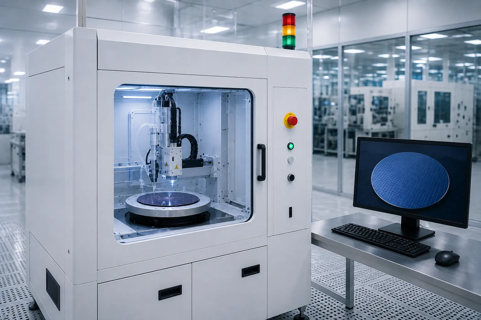 200 nm Standard · 100 nm Optimized
Single Wafer Cleaning Systems
Engineered for advanced node semiconductor fabrication where cross-contamination must be strictly eliminated. Integrates direct-drive spin chucks, multi-chemical delivery, targeted megasonic agitation, and IPA Marangoni drying.
- Enclosed mini-environment spin chambers with exhaust isolation
- Point-of-use chemical blend dispense with precise temp loops
- FEOL gate oxide, post-etch residue, and contact layer cleaning
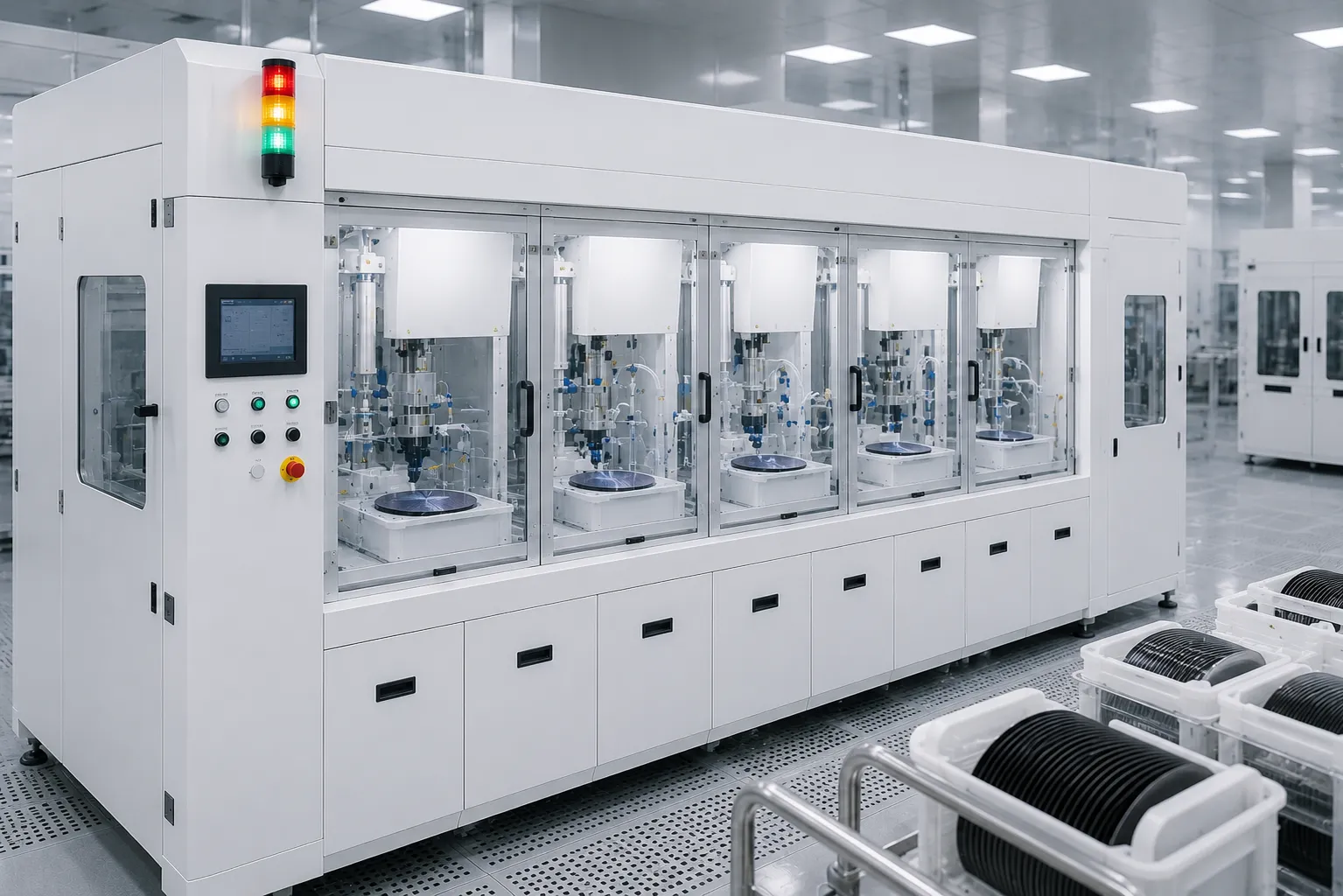 High-Volume Manufacturing
Batch Wafer Cleaning Systems
Automated multi-tank wet bench architectures designed for high-volume immersion cleaning, etching, and photoresist stripping. Delivers maximum wafer per hour (WPH) throughput while lowering chemical consumption.
- Continuous inline chemical concentration auto-dosing & filtering
- Cascading megasonic tanks with ultra-high purity recirculation
- Optimized for prime silicon substrate fabrication and reclaim lines
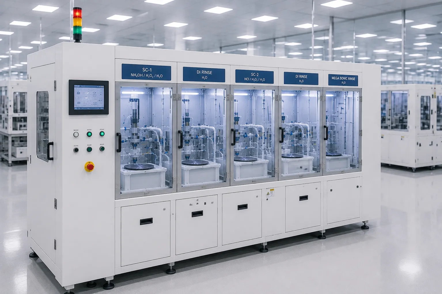 Proven Chemical Standard
RCA Cleaning Systems
Configured for classic and modified RCA clean sequences, including SC-1 (APM), SC-2 (HPM), SPM (Piranha), and DHF steps. Efficiently removes organic contaminants, fine particles, ionic metallic impurities, and native oxides.
- Standardized SC-1 and SC-2 process baths with megasonic support
- Sulfuric peroxide mixture (SPM) resist strip and organic breakdown
- Integrated high-efficiency quick-dump rinse (QDR) and IPA drying
Equipment Selection Guidelines for Semiconductor Wet Processing
Selecting the ideal wafer cleaning system requires balancing target yield specifications, substrate handling limits, and overall fab throughput objectives. While a high-precision single wafer cleaning system excels at eliminating cross-contamination during sensitive FEOL gate formation, contact clean, and 200 nm standard particle removal, optimized down to 100 nm, automated batch wafer cleaning systems offer unrivaled cost efficiency for raw wafer manufacturing, post-CMP cleaning, and reclaim wafer processing.
KOSEN SEMI builds all RCA cleaning systems and wet benches on modular chemical distribution frameworks. Featuring real-time bath concentration monitoring, fire-suppression systems, and full SEMI S2/S8 compliance, our equipment seamlessly integrates into modern ISO Class 5–7 cleanroom environments to protect both your process and your workforce.
Engineered for critical gate oxide preparation, contact hole cleaning, metal interconnect stripping, TSV packaging, and post-CMP wet processing.
Features dynamic inline chemical blending for HF, SC-1, SC-2, and specialized solvent chemistries, drastically reducing chemical waste and cost-of-ownership.
Customizable chucks and carrier-less transfer systems accommodate 100mm to 300mm Silicon, Silicon Carbide (SiC), Gallium Nitride (GaN), and ultra-thin substrates.
Breakthrough Wet Cleaning Innovations and Yield Protection
KOSEN SEMI engineers state-of-the-art Single Wafer Cleaning Systems designed to overcome extreme contamination challenges in 200 nm standard and optimized 100 nm semiconductor fabrication. By integrating dynamic megasonic energy modulation, ultra-low IPA Marangoni drying, and high-precision chemical dispensing, our proprietary wet process architecture maximizes particle removal efficiency while protecting vulnerable high-aspect-ratio microstructures from physical pattern collapse.
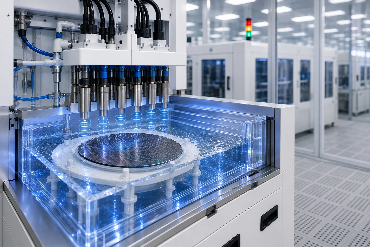
Uniform Megasonic Wafer Cleaning with Reduced Cavitation Damage Risk
Traditional acoustic cleaning frequently causes pattern collapse or micro-fractures in delicate high-aspect-ratio features due to erratic, uncontrolled transient cavitation. KOSEN SEMI solves this with proprietary dynamic megasonic wafer cleaning technology, modulating spatial acoustic wave distribution across the entire spinning substrate. This delivers maximum particle removal efficiency without degrading fragile gate structures or interconnect lines.
- Uniform Energy Density Matrix: Multi-frequency megasonic transducer arrays systematically prevent acoustic hot-spots and dead zones, providing consistent sound field coverage across 200mm and 300mm wafers.
- 200 nm Standard & 100 nm Optimized Particle Removal: Effectively dislodges particles down to 100 nm under optimized conditions while safeguarding sensitive FinFET, gate-all-around (GAA), and 3D NAND topologies from mechanical stress.
- Closed-Loop Power Modulation: Real-time acoustic sensors continually analyze power reflections, adjusting generator output in microseconds to match dynamic liquid film thickness and chemical composition.
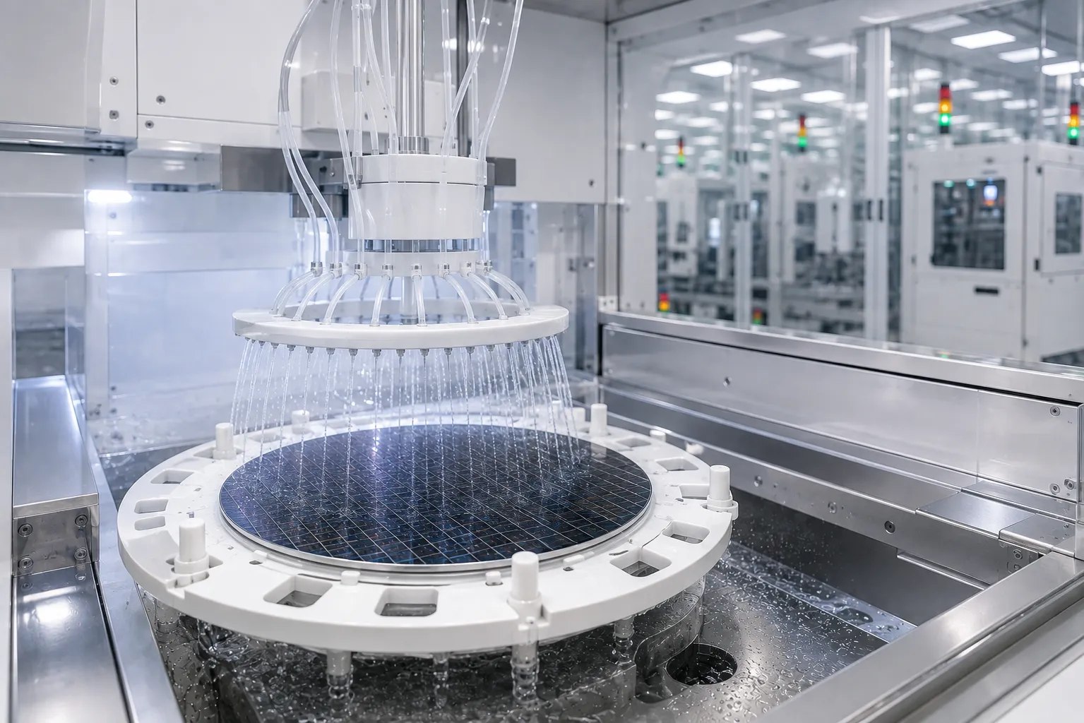
Low-Watermark Marangoni Drying with Ultra-Low Chemical Consumption
Thoroughly drying hydrophobic wafer surfaces without leaving chemical stains or watermarks is crucial for high-yield FEOL and BEOL wet processing. KOSEN SEMI incorporates advanced Marangoni drying technology, utilizing surface tension gradient dynamics to strip moisture cleanly from deep trenches and narrow vias while drastically reducing Isopropyl Alcohol (IPA) vapor consumption.
- Watermark Defect Control: Eliminates liquid meniscus entrapment and localized oxide stains across high-aspect-ratio contact holes and 3D TSV structures.
- Precision IPA Micro-Dosing: Intelligent mass flow controllers optimize IPA vapor concentration, reducing chemical volume consumption by up to 60% compared to conventional spin-rinse dryers.
- Inert Nitrogen Purge Micro-Environment: Maintains positive N2 pressure throughout the process chamber, eliminating airborne molecular contamination (AMC) and native oxide growth during drying.
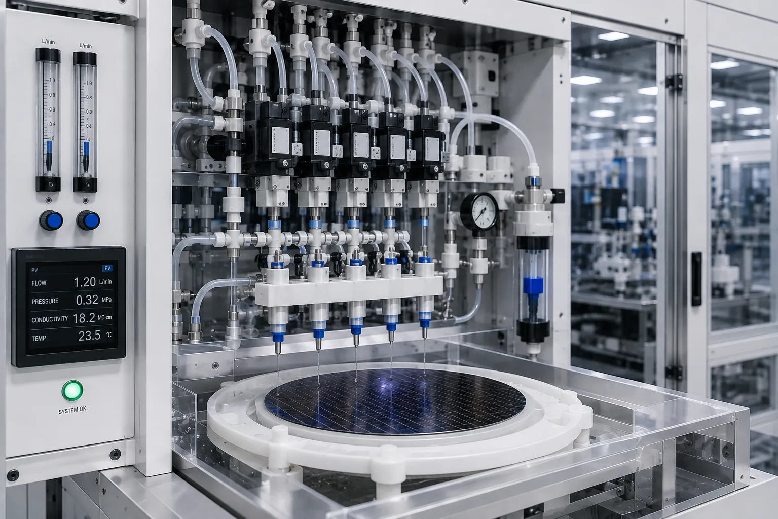
High-Precision Chemical Dispensing and Closed-Loop Flow Management
Achieving repeatable etch rates and surface cleanliness in RCA, SC-1, SC-2, and specialized solvent steps demands exact chemical concentration and thermal stabilization. KOSEN SEMI wafer cleaning systems feature an integrated chemical blending manifold with continuous closed-loop monitoring, ensuring chemical dispensing precision across every single wafer and batch cycle.
- In-Line Concentration Monitoring: High-resolution optical and spectroscopic sensors continuously measure active chemical concentrations (HF, H2O2, NH4OH) for real-time automated chemical spiking.
- Cross-Contamination Isolation: Fully segmented chemical fluidic paths and quick-response purge valves help minimize cross-contamination between corrosive acidic, alkaline, and solvent process steps.
- Ultra-Pure Fluoropolymer Fluidics: High-purity PFA and PTFE valves, tubing, and pumps eliminate metallic leaching and chemical degradation, extending equipment operational lifespan.
Ready to Elevate Your Wet Process Yield & Cleaning Efficiency?
Consult with KOSEN SEMI process engineers to discover how our megasonic cleaning, Marangoni drying, and precision chemical dispensing systems can be tailored to your fab line layout and defect density targets.
End-to-End Application Coverage in Semiconductor Fabrication
KOSEN SEMI engineers high-precision wafer cleaning systems tailored for every critical stage of modern silicon wafer fabrication. Our advanced semiconductor wet process equipment mitigates defect density, eliminates trace metallic cross-contamination, and delivers superior yield rates from initial substrate preparation through advanced packaging modules.
FEOL Surface Cleaning and Preparation
Critical Front-End-of-Line (FEOL) integration steps require atomic-scale surface purity to safeguard gate dielectric integrity. KOSEN SEMI equipment executes targeted single-wafer and automated batch RCA cleans to eliminate organic trace impurities and metallic contamination before gate oxide growth and ion implantation.
- Pre-Gate Oxide Cleaning: Removes organic trace impurities and thin native oxides without surface pitting.
- Post-Ion Implantation Strip: Clears hardened photoresist remnants and residual ions with precision.
- Optimized 100 nm Particle Control: Achieves high particle removal efficiency on sensitive nano-structures.
BEOL and Advanced Packaging Wet Processes
Modern Back-End-of-Line (BEOL) and 3D heterogeneous integration demand residue-free cleaning inside high-aspect-ratio microstructures. Our solutions solve complex FEOL and BEOL cleaning challenges, ensuring clean Through-Silicon Vias (TSV), pristine copper interconnects, and corrosion-free solder bump pads.
- TSV Deep Trench Cleaning: Thoroughly removes post-etch polymer build-up inside high-aspect micro-vias.
- Post-CMP Residue Removal: Eliminates slurry residues and metallic contaminants without chemical corrosion.
- Advanced Packaging Wet Process: Prepares wafer surfaces for micro-bumping, copper pillar plating, and direct bonding.
Compound Semiconductor Processing
Wide-bandgap materials require specialized fluid handling and damage-free physical agitation. We build dedicated wet systems optimized for SiC wafer cleaning and GaN processing that withstand highly aggressive chemistries while protecting brittle substrate edges.
- SiC Surface Oxidation Control: Supports controlled surface cleanliness prior to epitaxy growth.
- Harsh Chemical Compatibility: Fluoropolymer wetted components safely handle hot concentrated acids.
- Thin Substrate Protection: Non-contact megasonic energy delivery prevents fragile wafer fracturing.
Substrate Manufacturing and Wafer Reclaim
For raw silicon wafer slicing and test wafer recycling, operational throughput and chemical conservation are key performance drivers. KOSEN SEMI high-capacity wet processing benches streamline chemical turnover while achieving stringent particle count targets.
- Ingot Lapping Polish Cleaning: Removes heavy abrasive slurries and organic residues post-slicing.
- Wafer Reclaim Etching Strip: Efficiently strips dielectric films and metallic layers for wafer reuse.
- High Volume Throughput: Multi-cassette automated handling boosts total fab operational productivity.
Precision Contamination Control Across Complex Fabrications
Yield enhancement in modern semiconductor manufacturing depends directly on controlling micro-contaminants at each processing milestone. As device geometries shrink below 100 nm optimized process thresholds, even nano-scale organic films or trace metallic ions can lead to catastrophic gate dielectric breakdown or line shorts.
KOSEN SEMI platforms integrate automated chemical concentration monitoring, variable-frequency megasonic transducers, and low-watermark drying methodologies. By tailoring wet chemistry and hydrodynamic spray control to specific process nodes, our equipment minimizes structural pattern-collapse risk alongside industry-leading particle removal efficiency.
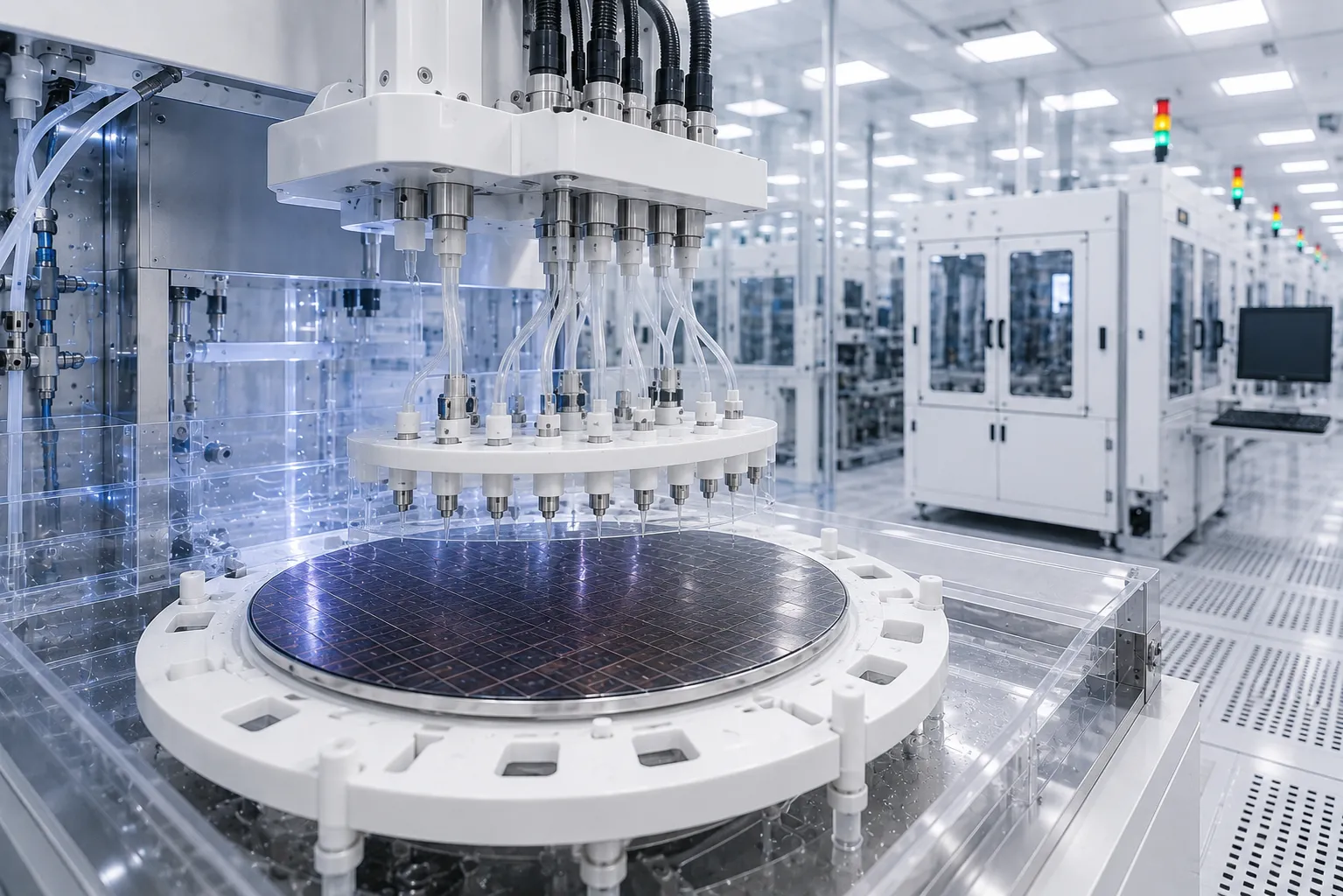
Wet Process Application Technical Matrix
Technical parameter alignment for semiconductor wet cleaning modules across core fab segments.
| Fab Process Segment | Primary Target Residues | Recommended Cleaning Technology | Supported Wafer Sizes |
|---|---|---|---|
| FEOL Gate Cleans | Organics, Native Oxides, Heavy Metals | Single Wafer Megasonic RCA + Chemical Spray | 200mm / 300mm (8 / 12 inch) |
| BEOL Post-CMP | Slurry Particles, Metallic Ions, Organic Residues | Dual-Sided Soft Brush Scrubber + Chemical Clean | 150mm / 200mm / 300mm |
| Compound (SiC / GaN) | Lapping Abrasives, Surface Oxides | Corrosion-Resistant Immersion Bench / Acoustic Clean | 100mm / 150mm / 200mm (4 / 6 / 8 inch) |
| Substrate & Reclaim | Bulk Polymers, Thin Film Stacks, Particle Swarms | High-Capacity Automated Batch Wet Bench | 150mm / 200mm / 300mm |
Wafer Cleaning Equipment Selection and Comparison Guide
Selecting the optimal semiconductor wet processing architecture is essential for maximizing yield, minimizing defect density, and balancing capital expenditure with ongoing chemical consumption. Fabs must evaluate critical trade-offs between single wafer isolation for advanced nodes and automated batch immersion for high-volume manufacturing. KOSEN SEMI manufactures advanced Single Wafer Cleaning Systems, fully automated Batch Wafer Cleaning Systems, and dedicated RCA Cleaning Systems lines engineered for precise process node integration and substrate geometries.
This technical framework evaluates key performance metrics across wet bench vs single wafer scrubber configurations to assist process engineers, yield specialists, and equipment procurement managers in making data-backed wafer cleaning equipment selection decisions.
Key Architectural Tradeoffs in Semiconductor Wet Processing
Fab line managers must balance particle removal efficiency (PRE) against total semiconductor wet equipment throughput. While single wafer scrubbers help minimize cross-contamination and protect delicate 100 nm optimized process structures, automated wet benches offer superior cost-efficiency for bulk chemical stripping, etching, and pre-furnace cleaning cycles.
- Yield & Defect Control: Single wafer isolation eliminates cross-contamination in critical FEOL gate oxide and contact cleaning stages.
- Throughput & Economics: Automated batch wet benches maximize wafer throughput per hour (WPH) for non-critical stripping and bulk etching.
- Chemical & CoO Optimization: Recirculated chemical baths with automated spiking reduce raw chemical consumption and operational costs.
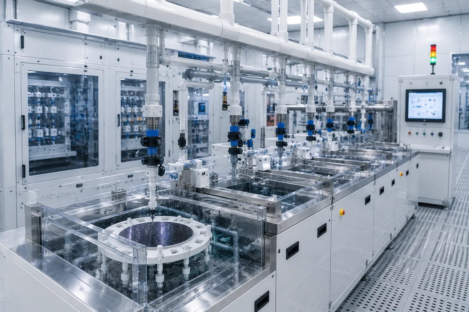
Interactive Equipment Selection Matrix
Filter performance benchmarks across single wafer, batch wet bench, and RCA cleaning architectures
| Evaluation Metric | Single Wafer Cleaning Systems | Automated Batch Wet Benches | RCA Chemical Cleaning Lines |
|---|---|---|---|
| Target Process Nodes | Optimized processes down to 100 nm | Standard processes at 200 nm and above | Standard substrate prep & legacy nodes |
| Wafer Size Compatibility | 150mm / 200mm / 300mm | 100mm / 150mm / 200mm / 300mm | 100mm / 150mm / 200mm / 300mm |
| Throughput Capacity | 30–60 WPH per chamber (multi-chamber setup) | 150–350 WPH high-volume production | 100–250 WPH batch chemical immersion |
| Particle Removal Efficiency | Optimized performance down to 100 nm particle sizes | Standard performance at 200 nm particle sizes | 98.5% for standard micro-particulates |
| Cross-Contamination Risk | Minimized (isolated single-wafer microenvironment) | Controlled (bath filtration & directional flow) | Controlled (real-time chemistry tank control) |
| Integrated Drying Technology | N2 / IPA Marangoni dry with megasonic assistance | Surface-tension Marangoni dry or spin dry | Hot N2 knife dry or standard spin rinse dryer |
| Chemical Dispensing Method | Point-of-use fresh chemical spray & acoustic nozzles | Recirculated chemical baths with online spiking | Sequential immersion tanks (SC-1, SC-2, dHF) |
| Primary Fab Applications | FEOL gate pre-clean, BEOL residue, advanced packaging | Bulk photoresist strip, oxide etch, wafer reclaim | Pre-oxidation clean, organic & metallic decontamination |
Single Wafer Cleaning Systems
Single wafer cleaning systems deliver precise, single-substrate isolation within sealed microenvironments. Engineered for advanced node FEOL and BEOL processing, these platforms combine megasonic energy control with point-of-use chemical dispensing to eliminate particles at 200 nm standard capability, optimized down to 100 nm without damaging fragile high-aspect-ratio microstructures.
- Optimized 100 nm Defect Control: High particle removal efficiency while mitigating pattern collapse on fragile microstructures.
- Cross-Contamination Control: Single-wafer isolation minimizes defect-transfer risk between high-value production wafers.
- Low-Watermark Drying: Integrated low-consumption IPA Marangoni drying modules eliminate liquid residue.
Automated Batch Wet Benches
Automated batch wet benches process multiple wafer cassettes concurrently inside high-purity chemical immersion baths. Designed for high-volume semiconductor fabrication, these wet benches offer exceptional economic efficiency for bulk chemical etching, resist stripping, and surface preparation where high wafer throughput is paramount.
- High Wafer Throughput: Processes up to 350 WPH via multi-axis robotic transfer and continuous bath operation.
- Optimized Chemical CoO: Recirculating chemical filtration systems with automated spiking minimize chemical consumption.
- Modular Tank Design: Fully configurable tank sequences supporting acid, solvent, and DI water rinse operations.
RCA Chemical Cleaning Lines
Standard RCA chemical cleaning lines utilize proven sequential chemical treatment using SC-1 ammonium hydroxide/peroxide and SC-2 hydrochloric acid/peroxide mixtures. Specialized for baseline wafer fabrication, these lines efficiently remove organic residues, light particulates, and trace metallic ionic contamination across diverse substrate materials.
- Benchmark Decontamination: Industry-standard chemistry sequence optimized for pre-oxidation and gate dielectric prep.
- Trace Metal Removal: Integrated complexing agents reduce metallic surface contamination down to sub-ppb levels.
- High Reliability & Uptime: Industrial-grade fluoropolymer construction delivers 98%+ system uptime with minimal maintenance.
Need Guidance on Equipment Selection?
Selecting between a single wafer scrubber and an automated batch wet bench depends on your target defect density, wafer size, process node, and overall fab footprint. Contact KOSEN SEMI application engineers for a comprehensive equipment configuration report and yield enhancement projection.
Semiconductor Equipment OEM Quality & Global Technical Support
KOSEN SEMI enforces strict manufacturing standards, factory wet-testing, and compliance across every wafer cleaning system for semiconductor manufacturing. Backed by an international technical support network, we deliver tool reliability and reduced unscheduled downtime.
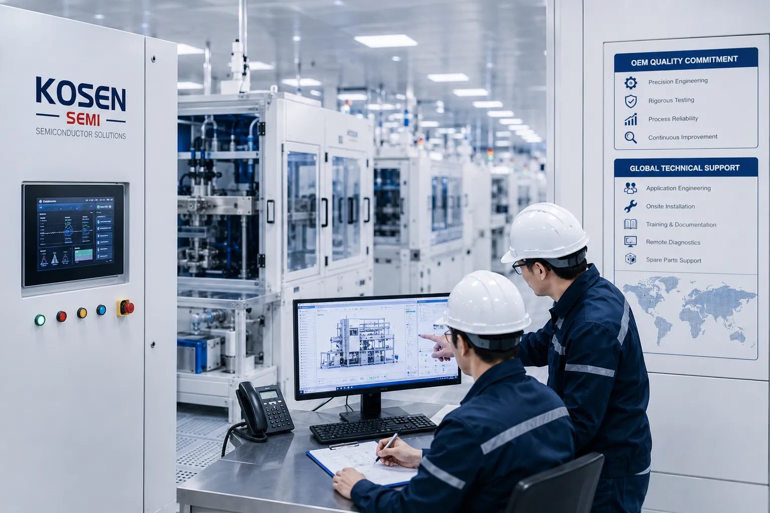
Precision assembly, automated optical inspection, and custom semiconductor equipment OEM integration within our advanced manufacturing facility.
Certified Engineering
Full compliance with SEMI S2/S8 standards, CE guidelines, and ISO 9001 quality management.
KOSEN SEMI Technical Support
24/7 remote guidance and rapid field engineer dispatch across key semiconductor fabrication hubs.
Rigorous Manufacturing Standards
100% pre-dispatch wet/dry testing and corrosion pressure validation.
Full Factory Acceptance Testing (FAT) and Site Acceptance (SAT) support.
Complete component batch traceability with high-purity material certification.
Wafer cleaning customization for specialized substrates and footprint constraints.
Quality Execution Timeline
End-to-end quality validation workflow ensuring yield stability and continuous tool uptime.
Incoming Quality Control (IQC)
Rigorous non-destructive testing and chemical compatibility verification for all fluidic components.
Cleanroom Precision Assembly
Micron-level mechanical alignment and sub-system integration within ISO Class 5–7 cleanrooms.
Pre-Shipment Wet & Dynamic Testing
Simulated production runs, automated chemical dispensing checks, and particle removal efficiency (PRE) validation.
Compliance Inspection & Serialization
SEMI S2/S8 compliance audit sign-off, complete FAT documentation, and permanent digital serial tracking.
Global On-Site Installation & SAT
Dedicated field engineers provide SAT verification, operator training, local spares inventory, and 24/7 service.
Explore Quality & Global Support Advantages
Custom Wafer Cleaning OEM
Tailored equipment configurations engineered for non-standard wafer sizes, specialized wet chemistry, and factory layouts.
Rigorous Testing Protocols
Every system undergoes comprehensive dry/wet stress trials and pressure leak checks before global dispatch.
Global Technical Service
Regional spare parts hubs and expert process engineers maintain tool availability and minimize unscheduled downtime.
Frequently Asked Questions: Wafer Cleaning Technology and Integration
Get clear answers to key technical questions regarding wafer fabrication cleaning process compatibility, equipment architecture, ROI, chemical handling, and qualification protocols. KOSEN SEMI application engineers support every tool from initial specification through site acceptance testing (SAT).
KOSEN SEMI wafer cleaning systems feature non-contact and low-stress handling technologies engineered specifically for fragile, warped, or ultra-thin substrates. Key transport safeguards include:
- Bernoulli-effect non-contact robotic end-effectors for wafers as thin as 50 µm
- Programmable contact-force edge-grip mechanisms that eliminate stress on active die areas
- Customizable vacuum and electrostatic chuck profiles for warped, bowed, or thin-film substrates
- Soft-landing spin chucks with dynamic RPM ramp control to eliminate edge chipping
- Flexible cassette-to-cassette or FOUP-compatible automation supporting 100 mm through 300 mm wafer formats
Every wafer transport sequence undergoes Factory Acceptance Testing (FAT) to verify slip-resistant, low-scratch handling performance prior to delivery.