
Single Wafer vs Batch Cleaning Architecture
As transistor geometries require stable processing at mature geometries, traditional batch wet processing reaches severe physical and chemical limitations in micro-defect control. KOSEN SEMI single wafer cleaning systems enforce microsecond fluid dynamic control over every individual wafer, eliminating cross-contamination and driving superior wafer-cleaning-systems performance for particle removal.
Limitations of Batch Wet Benches
Immersion chemical tanks process 25 to 50 wafers simultaneously in a shared liquid bath. Recirculated chemicals suffer from rapid concentration decay, thermal fluctuations, and particle accumulation, causing severe cross-wafer defect propagation at advanced nodes. For legacy nodes or specialized batch needs, explore our dedicated Batch Wafer Cleaning Systems.
- Cross-Contamination Risk: Particles, metallic ions, and organic impurities freely migrate between wafers in shared chemical tanks.
- Thick Boundary Fluid Layers: Slow fluid refresh rates prevent effective chemical exchange inside high-aspect-ratio trenches and patterns.
- Uncontrolled Edge Processing: Inability to isolate bevel film stripping or backside cleaning from active die regions on the frontside.
Single Wafer Precision Engineering
Single wafer processing isolates each substrate inside a dedicated process chamber. Point-of-use ultra-filtered fresh chemistry, targeted megasonic cavitation fields, and dynamic spin control eliminate micro-defects at the individual wafer level.
- Cross-Contamination Control: Point-of-use fresh chemistry delivery prevents re-deposition of micro-particles and metallic residues.
- Millisecond Flow Control: Millisecond switching between SPM, SC1, SC2, DHF, and functional gas-infused UPW streams.
- Targeted Bevel Cleaning: Non-contact Bernoulli clamping protects active devices during precise bevel and backside etching.
Overcoming Boundary Layer Stagnation and Defect Limits
In 200 nm standard semiconductor manufacturing and optimized processes down to 100 nm, the fluid boundary layer on static or slow-moving wafer surfaces hinders chemical reaction rates. Nanoparticles remain trapped within this stagnant fluid layer, escaping physical removal forces in standard batch immersion tanks.
KOSEN SEMI single wafer cleaning tools incorporate proprietary fluid dynamic nozzle arrays and high-speed spin chuck controls. Driven by our advanced Engineering Capability, our systems spin the wafer at optimized rotational velocities during chemical dispensing to dramatically thin the boundary layer. High-frequency megasonic waves propagate uniformly across the wafer radius, transmitting acoustic energy that supports 200 nm standard particle removal, optimized down to 100 nm, while minimizing structural pattern-collapse risk on fragile 3D NAND or Gate-All-Around (GAA) structures.
- Uniform Megasonic Energy Field: Eliminates acoustic energy hot spots to safeguard high-aspect-ratio structures.
- Marangoni Surface-Tension IPA Drying: Combines isopropyl alcohol (IPA) vapor gradients with spin speed to deliver low-watermark hydrophobic surfaces.
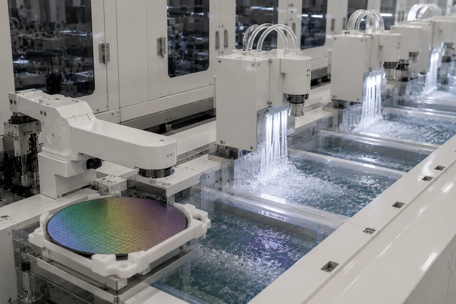
Precision Edge Bevel Etch and Backside Semiconductor Defect Control
Unwanted film build-up on wafer edges and backside particle contamination are leading causes of yield loss during photolithography, CMP, and thin-film deposition steps. While batch wet benches clean the entire wafer uniformly without spatial differentiation, single wafer systems offer absolute control over chemical contact zones.
KOSEN SEMI platforms utilize specialized dual-side and edge-bevel processing modules. Using non-contact vacuum or Bernoulli clamping chucks, active frontside dies remain protected under a continuous nitrogen purge or ultra-pure water barrier curtain. Simultaneously, precise micro-dispense nozzle arms apply etching chemistry to edge and bevel zones to strip unwanted oxide, nitride, metal, or organic films with sub-millimeter positioning accuracy.
Single Wafer vs Batch Cleaning Technical Comparison
Detailed performance comparison between legacy batch immersion wet benches and KOSEN SEMI high-precision single wafer cleaning systems.
| Parameter | Batch Immersion Systems | KOSEN SEMI Single Wafer Systems |
|---|---|---|
| Target Process Node | 200 nm standard processes | Optimized processes down to 100 nm |
| Particle Removal Efficiency (PRE) | Standard particle control at 200 nm | Particle control at 200 nm standard capability, optimized down to 100 nm |
| Chemical Refresh Mechanism | Recirculated shared tank baths | Fresh point-of-use chemical dispense |
| Edge and Bevel Control | None (Full wafer immersion) | Independent edge etch and bevel film strip |
| Cross-Contamination Risk | High (Inter-wafer fluid bath transfer) | Minimized (isolated single wafer chamber) |
| Drying Technology | Standard IPA vapor dryer / spin dry | Marangoni surface tension IPA spin dry |
| Chamber Configuration | Fixed multi-tank bath lines | Modular 4, 8, or 12 multi-chamber setups |
Optimized Total Cost of Ownership for High-Volume Fabs
While capital investment dynamics for single wafer cleaning tools differ from batch wet benches, the significant boost in die yield, reduction in scrapped wafers from minimized cross-contamination risk, and controlled chemical dosing yield a lower Total Cost of Ownership (TCO) at advanced process nodes. KOSEN SEMI single wafer cleaning platforms deliver the optimal combination of defect control, high throughput, and process reliability for modern 200mm and 300mm fabrication lines.
System Architecture & Core Technical Modules
KOSEN SEMI integrates advanced megasonic single wafer cleaning, precision chemical delivery, and low-watermark drying into a high-yield single wafer processing platform. Learn more about our overall Engineering Capability in semiconductor equipment.
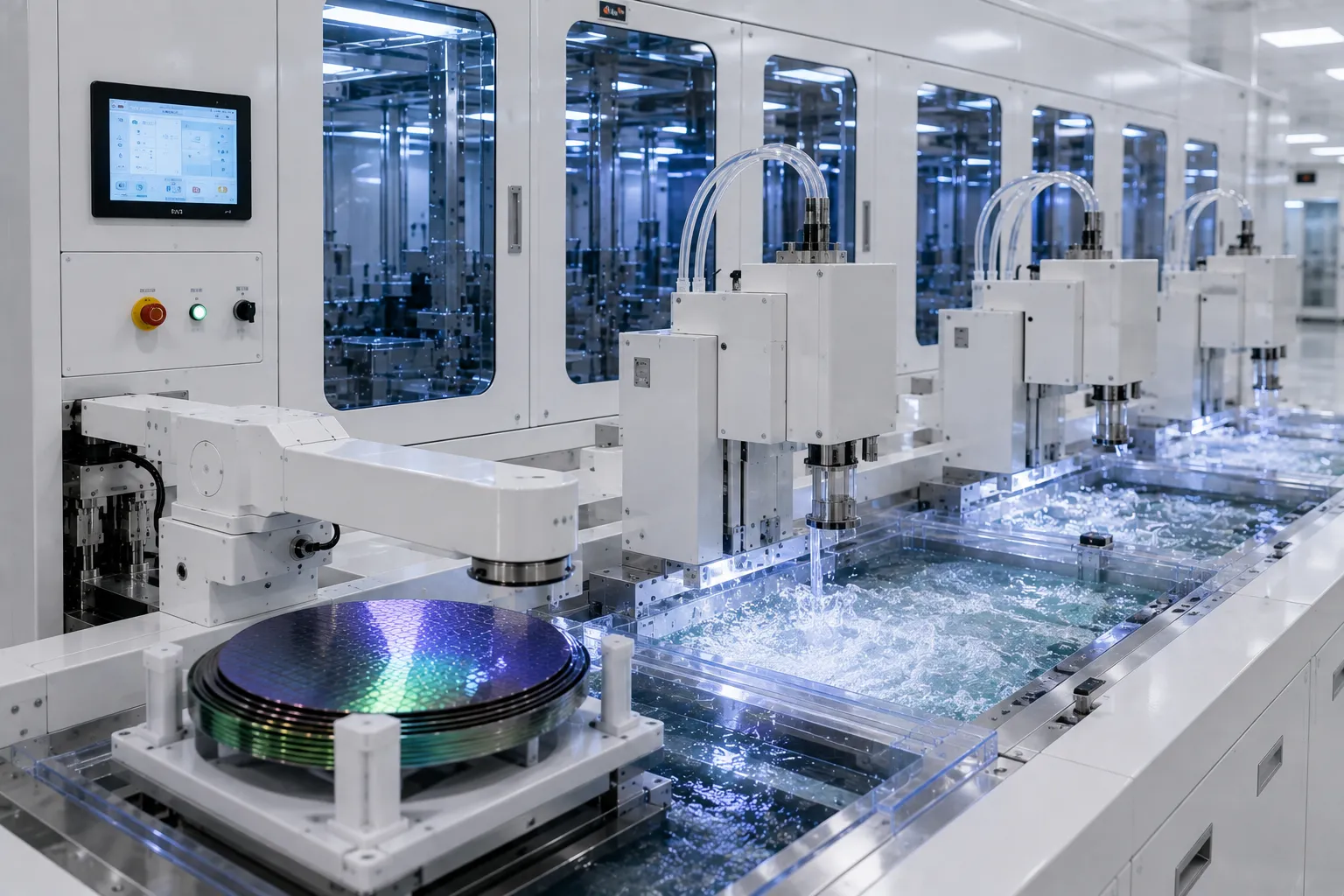
Advanced Contamination & Yield Control
Engineered for advanced node wafer fabrication, our single wafer cleaning tools integrate multi-frequency acoustic energy, dynamic chemical dispensing, and non-contact chucks to eliminate micro-defects and maximize process yield.
99.8%
Particle Removal Efficiency
<1 ms
Chemical Switch Response
Megasonic Single Wafer Cleaning Module
Delivers flexible, multi-frequency acoustic wave energy tailored to support 200 nm standard particle removal, optimized down to 100 nm, without causing structural collapse on fragile, high-aspect-ratio features. Compare with our Batch Wafer Cleaning Systems for high-throughput requirements.
- Prevents high-aspect-ratio pattern collapse
- Uniform acoustic energy distribution across 200mm & 300mm wafers
Precision Chemical Dispense Module
Provides sub-millisecond switching and exact flow rate control for SPM, SC1, SC2, DHF, and functionalized gas-infused ultra-pure water (UPW) chemistries.
- Sub-millisecond multi-chemical valve switching
- Integrated gas-infused UPW and micro-dosing systems
Low-Watermark IPA & Spin Dryer
Combines Marangoni surface tension gradient effects with high-speed rotation to support low-watermark drying across hydrophobic and hydrophilic surfaces.
- Low-watermark drying via Marangoni IPA gradient
- Optimized for complex hydrophobic and hydrophilic topographies
Dual-Side & Bevel Cleaning Chuck
Employs a non-contact Bernoulli vacuum chuck to isolate and protect active frontside die structures during back-side, edge, and bevel cleaning cycles.
- Non-contact Bernoulli clamping protects active dies
- Targeted edge-bevel etch and backside residue control
Precision Single Wafer Cleaning Across Advanced Semiconductor Nodes
As semiconductor device scaling requires tighter control at optimized 100 nm processes, controlling surface micro-defects demands nanosecond fluid mechanics, chemical precision, and minimized cross-contamination risk. KOSEN SEMI single wafer cleaning systems deliver tailored wet processing architectures that replace conventional Batch Wafer Cleaning Systems. By integrating focused megasonic energy, dynamic chemical dispense modules, and low-watermark IPA Marangoni drying, our solutions satisfy stringent defect-density requirements across front-end-of-line (FEOL), back-end-of-line (BEOL), and heterogeneous packaging nodes.
Optimized 100 nm Wafer Cleaning
Engineered specifically for gate-first and gate-last FinFET/GAA architectures, contact pre-cleaning, and post-CMP surface clearing. KOSEN SEMI advanced node wafer-cleaning-systems remove organic residues at 200 nm standard capability, optimized down to 100 nm, and metallic contaminants while preventing physical damage to fragile, high-aspect active device features.
- Pattern-Collapse Risk Control: Modulated megasonic energy distribution protects delicate FinFET fins and Gate-All-Around nanosheets from acoustic cavitation damage.
- Sub-Millisecond Chemical Switching: Sequential delivery of DHF, SC1, SC2, SPM, and ozonated water for controlled oxide etching and residual particle stripping.
- Post-CMP Particle Control: Exceeds 99.5% particle removal efficiency at 200 nm standard thresholds, optimized down to 100 nm, without film loss or surface roughness degradation.
3D NAND Trench and TSV Debris Flushing
Deep vertical channel etching and high aspect ratio geometries demand active chemical penetration and dynamic debris flushing backed by our advanced Engineering Capability. KOSEN SEMI single wafer cleaning systems combine synchronized fluid acoustic waves and gas-infused ultra-pure water to penetrate narrow memory trenches and Through-Silicon Vias (TSVs).
- Deep-Trench Penetration: Micro-bubble acoustics overcome capillary surface tension, thoroughly flushing slurry particles and etch polymers.
- TSV Bottom Cleaning: Complete removal of polymer residues and native oxide films prior to barrier layer deposition, ensuring optimal contact resistance.
- Marangoni Drying Integration: Eliminates watermark formation and chemical entrapment deep within high-aspect vertical memory cavities.
Compound Semiconductor & SiC Wafer Cleaning
Extremely hard Silicon Carbide (SiC) and Gallium Nitride (GaN) substrates present unique surface micro-roughness and stubborn post-polish slurry challenges. KOSEN SEMI offers specialized SiC wafer cleaning equipment that utilizes anti-corrosive chemical loops to deliver pristine substrate surfaces for high-yield epitaxial layer growth.
- Epi-Ready Surface Quality: Removes heavy metal ions and polishing slurry particles to high-purity surface cleanliness targets.
- Bevel & Edge Chemical Isolation: Independent chemical etch control prevents substrate edge flaking, micro-chipping, and particle generation.
- Corrosion-Resistant Hardware: Fluoropolymer processing chambers specifically engineered to withstand aggressive SPM, hot acids, and HF chemistry.
Advanced Packaging and Flux Residue Removal
High-density micro-bump arrays, copper pillars, and redistribution layers accumulate stubborn flux residues, photoresist scum, and organic films. KOSEN SEMI single wafer tools deliver high-impact directional chemical spraying to clear micro-gap contaminants prior to die bonding.
- Photoresist Scum Stripping: Complete solvent flushing across tight-pitch micro-bumps without undermining delicate solder caps.
- Non-Contact Bernoulli Chuck: Complete frontside pattern protection during thin-wafer handling, stress relief, and backside spin cleaning.
- Enhanced Interconnect Reliability: Prevents micro-voiding and electromigration failures in advanced heterogeneous chiplet integration.
Seamless Integration for 200mm Retrofits and 300mm Greenfield Fabs
Whether retrofitting legacy 200mm fabrication lines to maximize operational efficiency or equipping state-of-the-art 300mm wafer fabrication equipment for high-volume manufacturing, KOSEN SEMI provides scalable, modular single wafer tool configurations tailored to your cleanroom layout.
Compact physical footprint engineered to replace legacy wet benches without altering existing fab infrastructure or piping.
Up to 12 configurable processing chambers with dual-arm robotic handling delivering up to 300+ WPH operational throughput.
Fully compliant with SEMI S2, S8, and ISO Class 5–7 cleanroom operational standards for seamless global fab deployment.
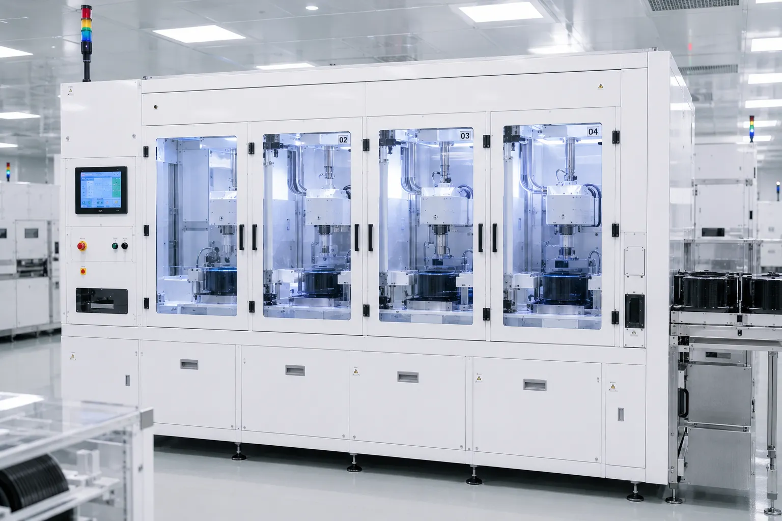 Figure 1: KOSEN SEMI High-Yield Process Chamber Isolation
 Technology Node Process Capability Matrix
Comparison of KOSEN SEMI single wafer cleaning capabilities across key semiconductor manufacturing nodes.
| Process Node / Scenario | Target Defect Size | Primary Chemistry | Drying Technology | Particle Removal Efficiency |
|---|---|---|---|---|
| 200 nm Standard / 100 nm Optimized Logic Processes | 200 nm Standard / 100 nm Optimized Particles | DHF, SC1, SC2, SPM, Gas-UPW | High-Speed Marangoni IPA | 99.5% |
| 3D NAND Flash (>128 Layer) | Trench Slurry Residues | Functionalized O3/UPW, Dilute Acids | Surface-Tension IPA Spin | 99.2% |
| Wide-Bandgap (SiC / GaN) | Polishing Slurry & Metals | Aggressive Hot SPM, Hydrofluoric Acid | High-RPM Nitrogen Spin Dry | 99.0% |
| Advanced Packaging & Bump | Flux & Photoresist Scum | Specialized Solvent Strippers, SC1 | Marangoni IPA Dry | 99.8% |
* Note: All operational metrics verified in ISO Class 5–7 cleanroom test facilities operating under SEMI S2 and S8 safety standards. Custom chemical dispense sequences are available upon request.
Single Wafer Cleaning Tool Specs & Performance Matrix
Engineered for advanced semiconductor manufacturing. Evaluate key single wafer cleaning systems tool specs across standardized modular platforms or fully customized chamber layouts tailored to your fab constraints.
Standardized Modular Platforms
Pre-configured architectures designed for rapid fab integration, predictable process repeatability, and seamless throughput scaling across high-volume production lines.
Customized Chamber Layouts
Tailored chamber positioning and specialized fluid manifold routing engineered specifically for strict cleanroom footprint limitations and complex process sequences.
KOSEN SEMI Single Wafer Cleaning Tool Specs
Comprehensive architectural parameters for throughput single wafer cleaner selection
| Matrix Parameter | Specification Range | Fab Performance Benefit |
|---|---|---|
| Wafer Size Compatibility | 200mm (8-inch) & 300mm (12-inch) | Multi-substrate capability supporting both legacy high-volume fab lines and advanced node wafer manufacturing. |
| Chamber Configuration | 4, 8, or 12 Multi-Chamber Setups | Scalable platform architecture engineered to balance complex chemical sequences with target production volumes. |
| Maximum Throughput | Up to 300+ WPH | High-speed robotic transfer and optimized fluid dispense cycles deliver maximum throughput single wafer cleaner output. |
| Particle Removal Efficiency (PRE) | Particle control at 200 nm standard capability, optimized down to 100 nm | Superior micro-defect elimination for 200 nm standard processes, optimized down to 100 nm, protecting yield on delicate logic and memory features. |
| Chemical Compatibility | Full Resistance: SPM, SC1, SC2, DHF, Solvents | Validated structural and fluidic integrity across aggressive acid, base, and organic solvent wet chemistry sequences. |
| Drying Technology | Marangoni & IPA Spin Dry Options | low-watermark surface drying engineered for sensitive, high-aspect-ratio wafer features and fragile patterns. |
| Cleanroom Footprint | Compact Fab Footprint Optimization | Maximized tool productivity per square meter of expensive ISO Class 5–7 cleanroom floor space. |
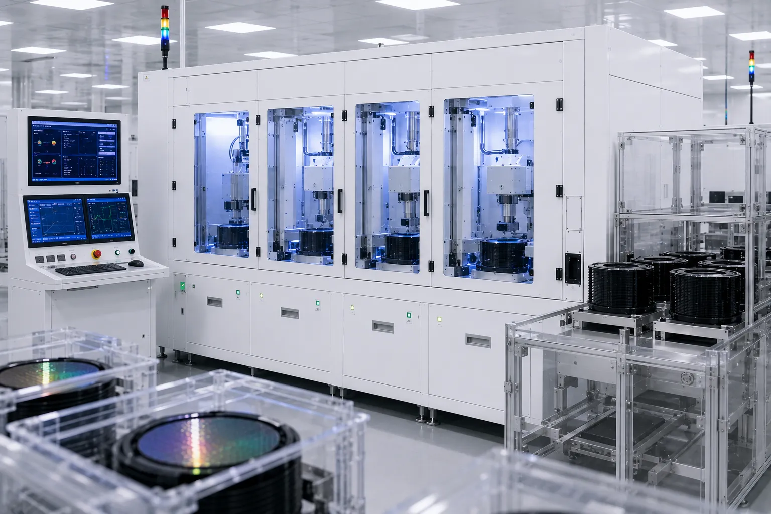
Integrated Architecture for High-Yield Fab Operations
KOSEN SEMI single wafer cleaning systems combine precision hardware engineering with intelligent process control. Backed by our advanced Engineering Capability, every platform is designed to lower total cost of ownership while maintaining low defect density across critical manufacturing steps.
Scale seamlessly from 4 to 12 chambers as output needs grow.
Advanced particle controls protect critical optimized 100 nm process structures.
Corrosion-resistant materials support aggressive acid and solvent chemistries.
Optimized tool dimensions maximize output per cleanroom square meter.
Need Custom Chamber Engineering?
KOSEN SEMI application engineers specialize in adapting tool configurations and single wafer cleaning tool specs to match non-standard cleanroom footprints and proprietary chemical process flows.
Cleanroom Certified Cleaning System Standards and Quality Assurance
Semiconductor fab yield depends directly on tool reliability, process repeatability, and absolute micro-defect mitigation. As feature sizes require tighter control at optimized 100 nm processes, microscopic surface contaminants and chemical cross-contamination can severely jeopardize wafer output. As an established semiconductor wet process supplier, KOSEN SEMI manufactures single wafer cleaning equipment inside certified ISO Class 5–7 cleanroom environments, adhering strictly to global capital equipment regulations, safety standards, and environmental compliance.
By combining ultra-pure hardware construction, closed-loop sensor automation, and comprehensive analytical process validation, KOSEN SEMI provides semiconductor fabrication facilities worldwide with maximum operational uptime, stringent defect control, and total compliance with our advanced wafer-cleaning-systems.
Global Semiconductor Equipment Compliance Standards
Every KOSEN SEMI single wafer processing tool is fully designed and certified to comply with SEMI S2 (Environmental, Health, and Safety) and SEMI S8 (Ergonomic Engineering) standards. Tool enclosures feature redundant chemical containment, automated leak detection, and localized exhaust management to safeguard cleanroom operators and environment integrity.
Precision assembly and testing occur exclusively within our advanced manufacturing-facility and ISO Class 5–7 cleanroom facilities, minimizing airborne particle contamination risk during manifold routing and fluidic integration.
Rigorous Quality Assurance Framework
High-purity surface cleanliness begins at the material interface. KOSEN SEMI conducts 100% component-level chemical compatibility testing on all PFA, PTFE, and specialized fluoropolymer fluid lines prior to integration.
Fully automated closed-loop sensor calibration supports precise chemical dispensing, dynamic temperature control, and real-time trace contamination monitoring. Continuous telemetry tracking prevents process drift, securing predictable 200 nm standard wafer defect control, optimized down to 100 nm across high-volume manufacturing runs.
Advanced Process Application Lab Support
Fabs evaluating a high-precision SEMI S2 compliant wafer cleaner gain full access to KOSEN SEMI state-of-the-art process application laboratories. Our senior wet process engineers conduct customized sample cleaning trials tailored to your specific process chemistries and defect profiles, backed by our world-class Engineering Capability.
Every trial yields exhaustive pre-clean and post-clean analytical reports to confirm Particle Removal Efficiency (PRE) performance and material selectivity prior to tool deployment.
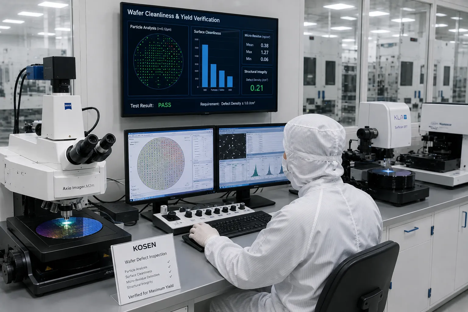
In-House Metrology and Wafer Defect Analysis Verification
Our specialized process application labs deploy industry-leading analytical metrology equipment to verify that every single wafer cleaning system satisfies customer yield requirements. Trial results provide transparent, quantified data regarding surface cleanliness, micro-residue, and structural integrity.
- Scanning Electron Microscopy (SEM): Inspects high-aspect-ratio surface features and nanoscale topography to verify particle removal at 200 nm standard capability, optimized down to 100 nm without causing pattern collapse.
- Atomic Force Microscopy (AFM): Measures surface roughness topography down to angstrom-level resolution, confirming minimized substrate etch erosion or degradation.
- X-Ray Photoelectron Spectroscopy (XPS): Analyzes elemental surface composition to verify removal of trace metallic impurities and organic chemical residues.
Compliance and Quality Verification Matrix
| Compliance Category | Standard Specification | Verification Protocol | Fab Impact |
|---|---|---|---|
| Environmental & Safety | SEMI S2 / SEMI S8 Certified | Third-party EH&S audit and fail-safe interlock testing | Reduced chemical exposure risk with multilayer operator safeguards |
| Cleanroom Standards | ISO Class 5–7 Manufacturing | Continuous airborne particle monitoring per ISO Class 5–7 procedures | Elimination of airborne particulates during tool construction |
| Fluidic Integrity | 100% PFA/PTFE Chemical QA | Pressure decay, ultra-pure water flush, and chemical soak tests | Minimized chemical leaching and cross-contamination risk |
| Analytical Defect Control | SEM / AFM / XPS Verified | Pre- and post-clean defect mapping at 200 nm standard capability, optimized down to 100 nm | Target >99.5% PRE under validated conditions for advanced FEOL and BEOL nodes |
Apply for Complimentary Wafer Sample Testing Services
Validate KOSEN SEMI single wafer cleaning performance on your actual production substrates. Submit your target process node requirements to receive a comprehensive defect analysis report and feasibility study from our application engineers within 24 hours.
Configure Your Custom Wafer Cleaning Solution & Estimate System ROI
Select wafer dimensions, process objectives, and throughput targets to streamline your wet processing tool selection and receive an instant chamber configuration proposal and budget analysis.
200mm / 300mm / Specialty
200 nm Standard · 100 nm Optimized / Metal Clean / Drying
High-Yield Benchmarking
Output models chemical consumption, cleanroom footprint allocation, and capital payback periods based on semiconductor industry benchmarks. Learn more about-us and our tailored equipment support.
24-Hour Process Feasibility Response Target
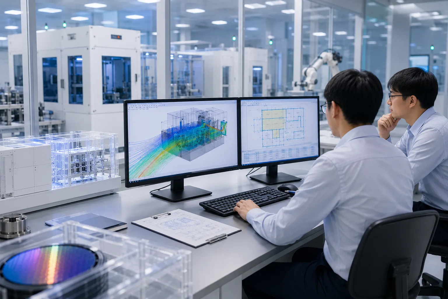
KOSEN SEMI application engineers analyze your evaluation inputs within 24 hours to deliver custom process feasibility studies and Cost of Ownership (COO) models.
- Custom chemical dispense & hydrodynamic flow modeling
- Cleanroom footprint, exhaust, & utility integration review
- Detailed Cost of Ownership (COO) & payback analysis
FEOL 200 nm Standard · 100 nm Optimized Platforms
Single-wafer wet processing architectures engineered for strict defect control and ultra-clean surface preparation.
BEOL & Specialty Etch Systems
Versatile chemical dispense platforms for post-etch residue removal, bevel cleaning, and advanced packaging.
Drying & Surface Conditioning
Advanced low-watermark Marangoni IPA drying technology designed for delicate, high-aspect-ratio wafer microstructures.
Single Wafer Processing Frequently Asked Questions
Explore how KOSEN SEMI single wafer cleaning systems solve critical wafer cleaning defect control challenges, optimize chemical usage, and maintain high throughput across advanced semiconductor fabrication nodes.
Total Cost of Ownership Comparison
While initial capital expenditure for single wafer systems is higher than legacy Batch Wafer Cleaning Systems, single wafer equipment yields significantly lower Total Cost of Ownership (TCO) in advanced semiconductor manufacturing nodes. Single wafer processing eliminates batch-wide scrap risk while enabling precise chemical dispense module management.
Elevated chemical reuse rates and point-of-use dispensing reduce chemical consumption by up to 35 percent across SPM, SC1, SC2, and DHF steps.
Isolated chamber processing reduces batch-wide cross-contamination and catastrophic wafer-loss risks.
Particle removal at 200 nm standard capability, optimized down to 100 nm, supports consistent device yield.
Throughput and Wafer Per Hour Rates
High throughput is achieved through multi-chamber parallel processing architectures, rapid handling robotics, and optimized multi-chemical spray delivery systems designed to meet high throughput single wafer cleaner requirements.
- Multi-Chamber Parallel Processing: Configurable tool platforms support 4, 8, or up to 12 independent processing chambers within a compact cleanroom footprint.
- Dual-Arm Handling Robotics: High-speed wafer transfer arms minimize handling overhead and cycle times between chambers.
- Millisecond Chemical Switching: Advanced fluidic manifolds allow ultra-fast switching between SPM, SC1, SC2, DHF, and functionalized gas-infused UPW rinses.
- High WPH Performance: Engineered configurations achieve high operational availability and throughput speeds exceeding 300 wafers per hour.
Aggressive Chemical and Solvent Compatibility
KOSEN SEMI single wafer tools feature total fluidic isolation and high-purity construction materials designed to safely handle demanding semiconductor wet etch and cleaning chemistries while simplifying semiconductor wet bench maintenance routines.
Process chambers, chemical lines, and fluid delivery modules are constructed using high-purity PFA, PTFE, and specialized fluoropolymers. Isolated local exhaust ventilation systems safely manage fumes during aggressive SPM mixtures, hydrofluoric acid etching, organic solvent stripping, and alkaline rinses.
Particle Removal Efficiency and Defect Control
KOSEN SEMI equipment integrates megasonic single wafer cleaning transducers, controlled fluid dynamics, and high-speed Marangoni IPA spin drying to achieve over 99.5 percent particle removal efficiency at 200 nm standard capability, optimized down to 100 nm.
Acoustic energy distribution minimizes pattern-collapse risk on delicate high-aspect-ratio features, while non-contact Bernoulli clamping chucks isolate sensitive frontside die structures during backside and bevel cleaning operations.
Global Field Service and Yield Optimization Support
KOSEN SEMI provides full technical support for wet processing capital equipment installations. Semiconductor fabs gain direct access to global field engineering teams, rapid spare parts deployment, routine semiconductor wet bench maintenance, and full application lab testing services.
Submit sample wafers for pre- and post-clean SEM, AFM, and XPS defect analysis reports.
Build a Single Wafer Cleaning System Around Your Exact Process Requirements
Work with KOSEN SEMI engineers to configure wafer handling, chemical sequences, particle removal, drying, automation, and throughput around your fab process, wafer size, and cleanroom integration requirements.