
Semiconductor Wet Process Applications & Wafer Processing Hubs
Delivering precision wet cleaning, chemical etching, and surface conditioning solutions across front-end IC fabrication, advanced packaging, compound semiconductors, and MEMS.
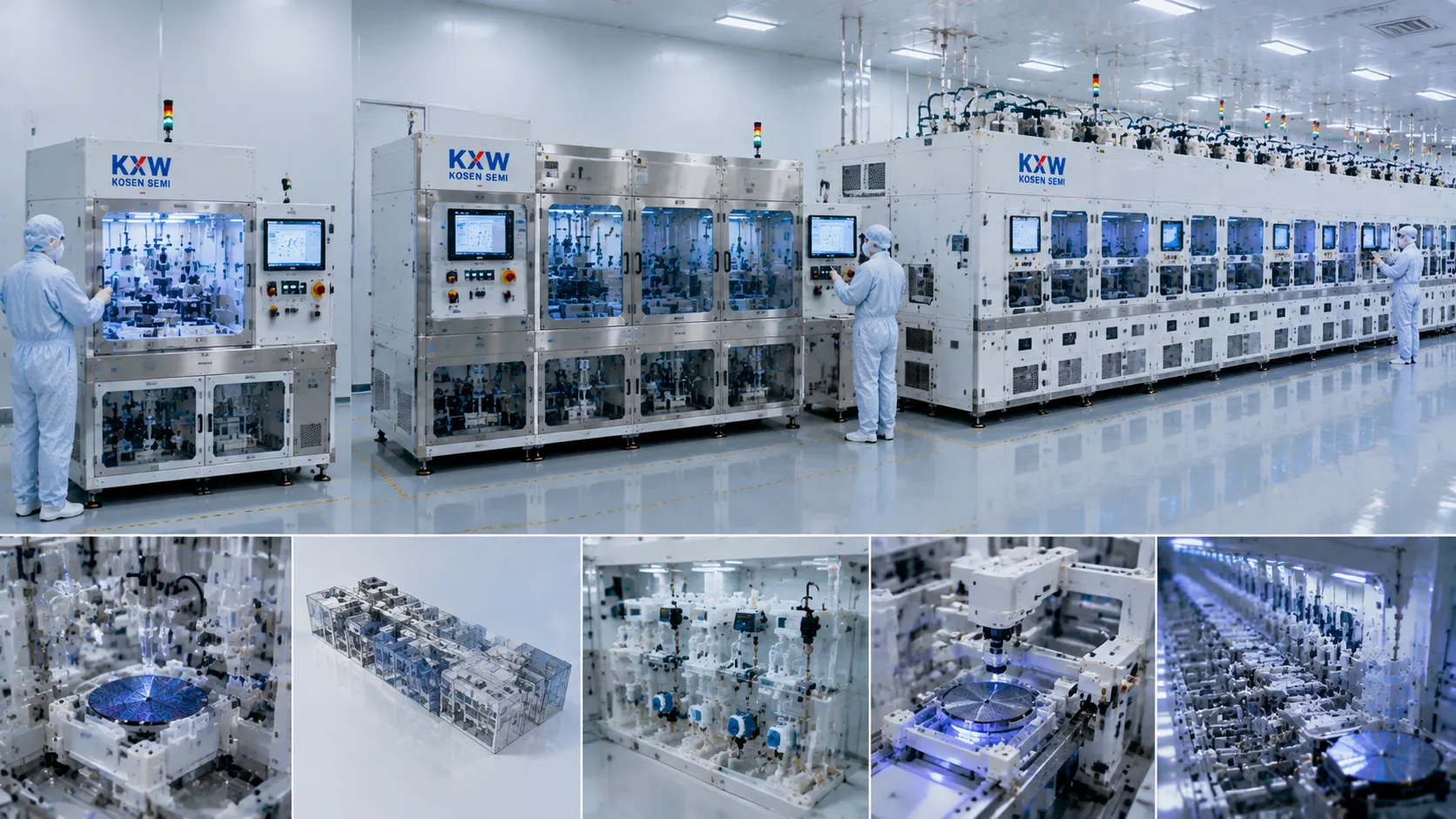
KOSEN SEMI specializes in advanced semiconductor wet process equipment, engineering high-yield solutions for demanding global fabrication environments. Learn more about-us to see how we power microelectronics manufacturing.
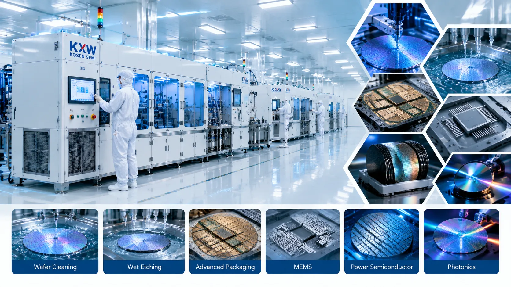
Front-End Semiconductor Manufacturing & Wafer Fabrication
Front-end semiconductor manufacturing demands rigorous chemical precision, uncompromising cleanliness, and total process repeatability across every processing step. As integrated circuit features shrink to advanced nodes, defect control during critical wet etch, surface preparation, and cleaning operations directly governs overall wafer fabrication yield. Built on decades of high-volume fab experience and our advanced manufacturing facility, KOSEN SEMI wet process systems are engineered for high-yield IC manufacturing lines, offering seamless tool integration, precise chemical dosing, and superior contamination control across diverse substrate materials.
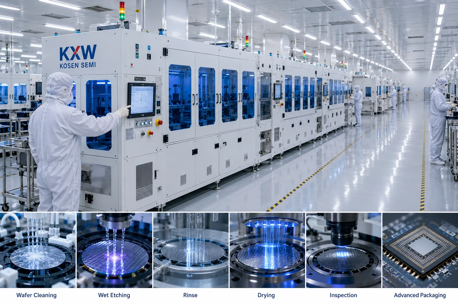
Semiconductor Manufacturing
Modern semiconductor manufacturing workflows require adaptable wet processing hardware capable of executing critical RCA cleans, oxide stripping, and pre-gate surface preparation. KOSEN SEMI toolsets integrate directly into automated material handling systems (AMHS) and SECS/GEM host networks, ensuring stable substrate transfer, controlled cross-contamination risk, and continuous high-volume production.
Core Yield Parameters
- ✓ Substrate compatibility across Si, SiC, and GaN wafers
- ✓ Fully automated recipe execution with inline chemical dosing
- ✓ Zero-cross-contamination chemical isolation architecture
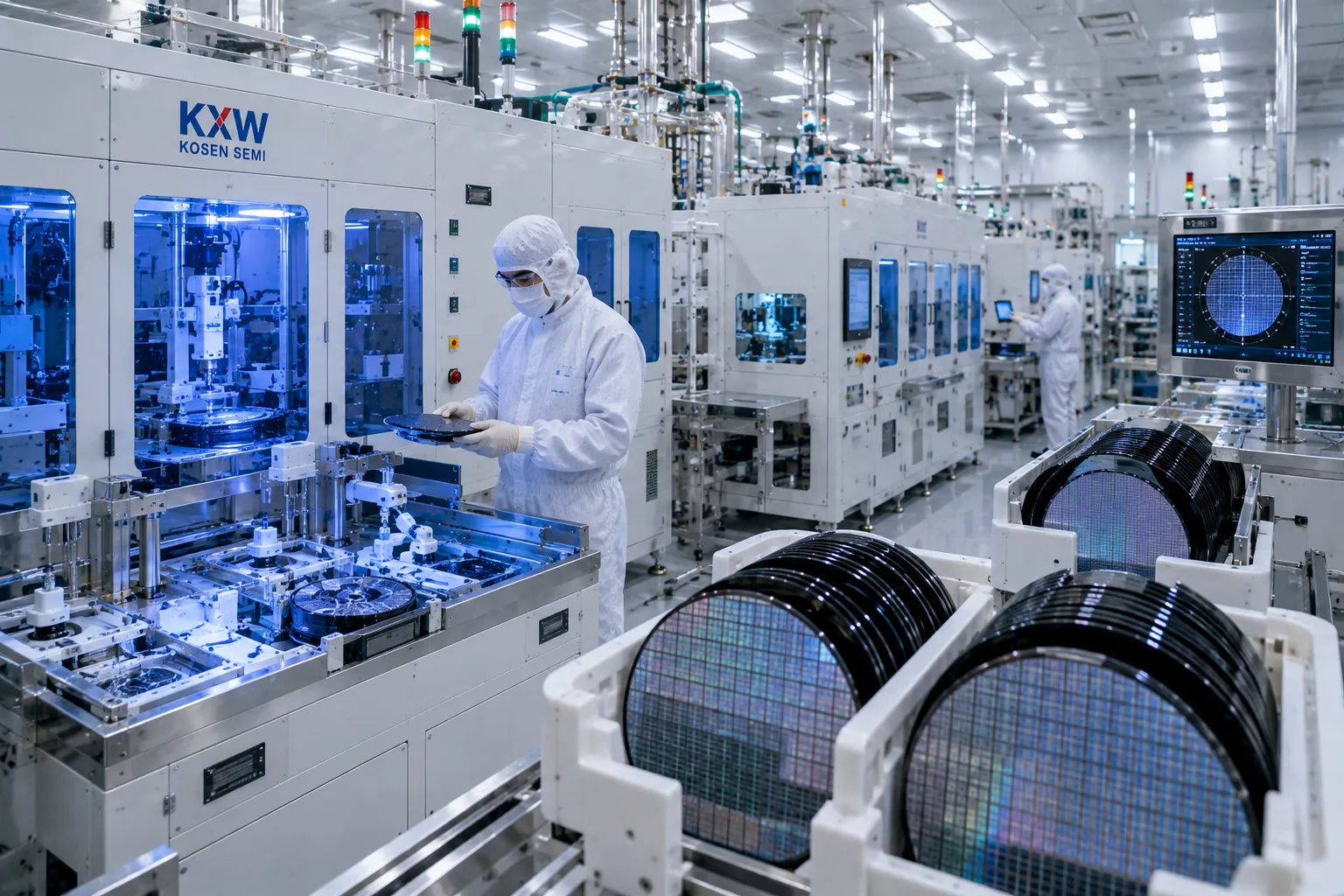
Wafer Fabrication
Engineered specifically for high-volume wafer fabrication facilities, our automated wet benches and single wafer cleaning systems easily adapt to 200mm (8-inch) and 300mm (12-inch) fab configurations. Advanced CFD-modeled fluid dynamics deliver uniform chemical bath replenishment, precise temperature regulation, and reduced chemical consumption across complex wafer lots.
Core Yield Parameters
- ✓ Flexible 200mm and 300mm dual-bridge or dedicated tool designs
- ✓ High-precision thermal bath control within ±0.5°C
- ✓ Targeted megasonic energy delivery for trench cleaning
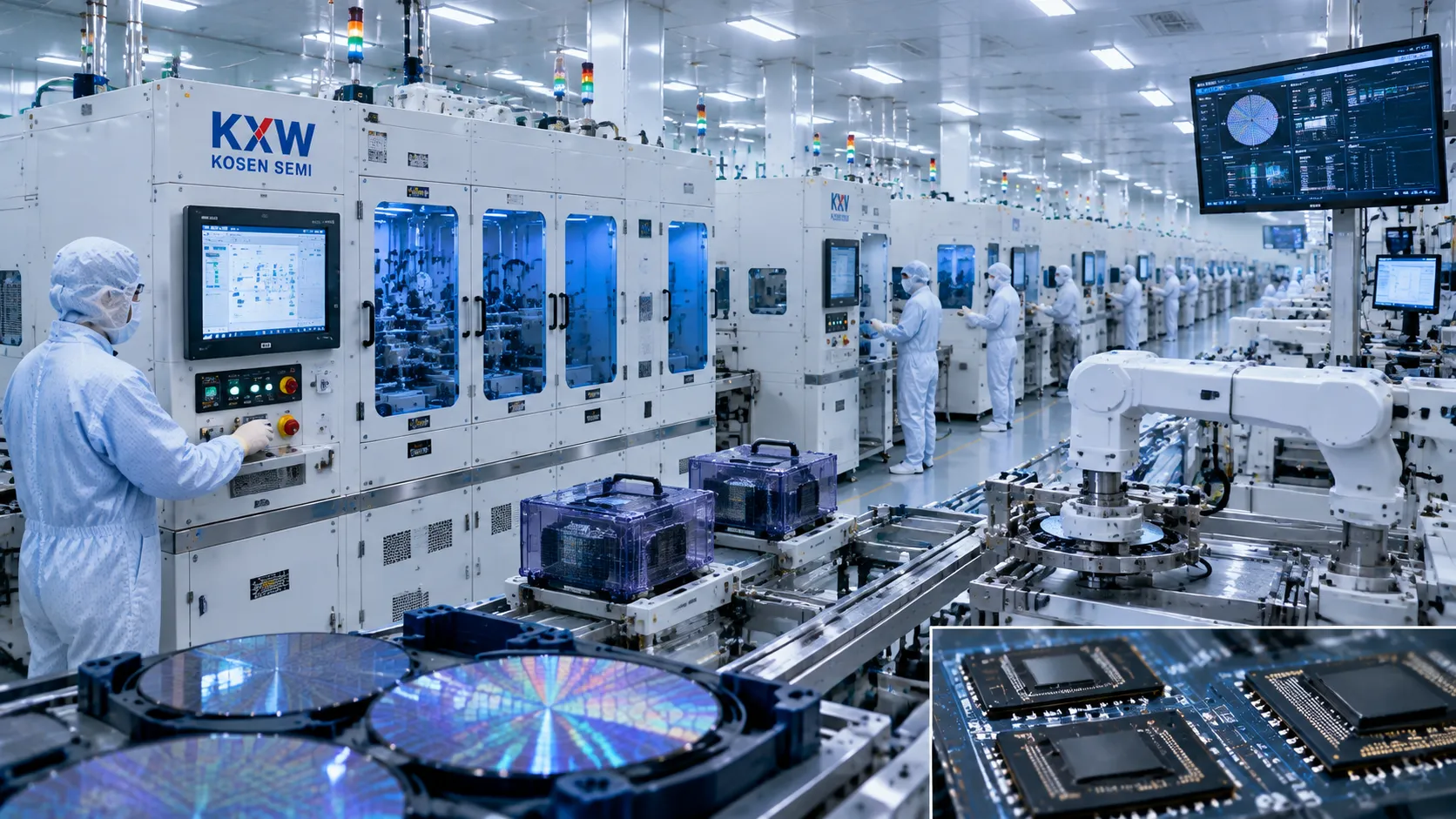
IC Manufacturing
Ultra-clean IC manufacturing requires absolute suppression of Airborne Molecular Contamination (AMC), 200 nm-class particle removal, with optimized capability down to 100 nm, and controlled trace metallic impurity removal. Featuring enclosed micro-environments and high-purity chemical supply channels, KOSEN SEMI equipment prevents defect propagation on active device layers to maximize line yield.
Core Yield Parameters
- ✓ Particle removal down to 100 nm under optimized conditions, with efficiency verified by application testing
- ✓ Trace metallic impurity control suppressed below 1E10 atoms/cm²
- ✓ Integrated mini-environment with ULPA filtration and N2 purging
Front-End Wet Process Integration & Capability Overview
Selecting the optimal wet processing tool architecture depends on wafer diameter, target throughput, chemical compatibility, and device node sensitivity. The matrix below demonstrates how KOSEN SEMI platforms address core wafer fabrication and semiconductor manufacturing demands to maintain superior yields while lowering total cost of ownership (TCO).
| Application Sector | Primary Equipment Architecture | Contamination Target | Fab Yield Impact |
|---|---|---|---|
| Universal Semiconductor Manufacturing | Automated Multi-Tank Wet Bench System | Cross-Contamination & Polymer Residue Removal | +1.2% Total Line Yield |
| 200mm / 300mm Wafer Fabrication | Single-Wafer Cleaner & High-Speed Scrubber | 200 nm-Class Slurry & Etch Particle Defect Control | 35% Reduction in Particle Defects |
| Ultra-Clean IC Manufacturing | Enclosed Single-Wafer System with Megasonics | Trace Metallic Impurities & Airborne AMC | < 1E10 atoms/cm² Purity Standard |
Advanced Packaging, Power Devices & MEMS Systems
High-density back-end integration requires efficient chemical exchange and strict micro-contamination control. With an unwavering customer-first focus, KOSEN SEMI incorporates custom fluid dynamics tailored for 3D packaging, power semiconductor manufacturing, and MEMS architectures, delivering superior chemical exchange in high-aspect-ratio structures to maximize yield across next-generation fabrications. Learn more about us and our dedicated engineering capabilities.
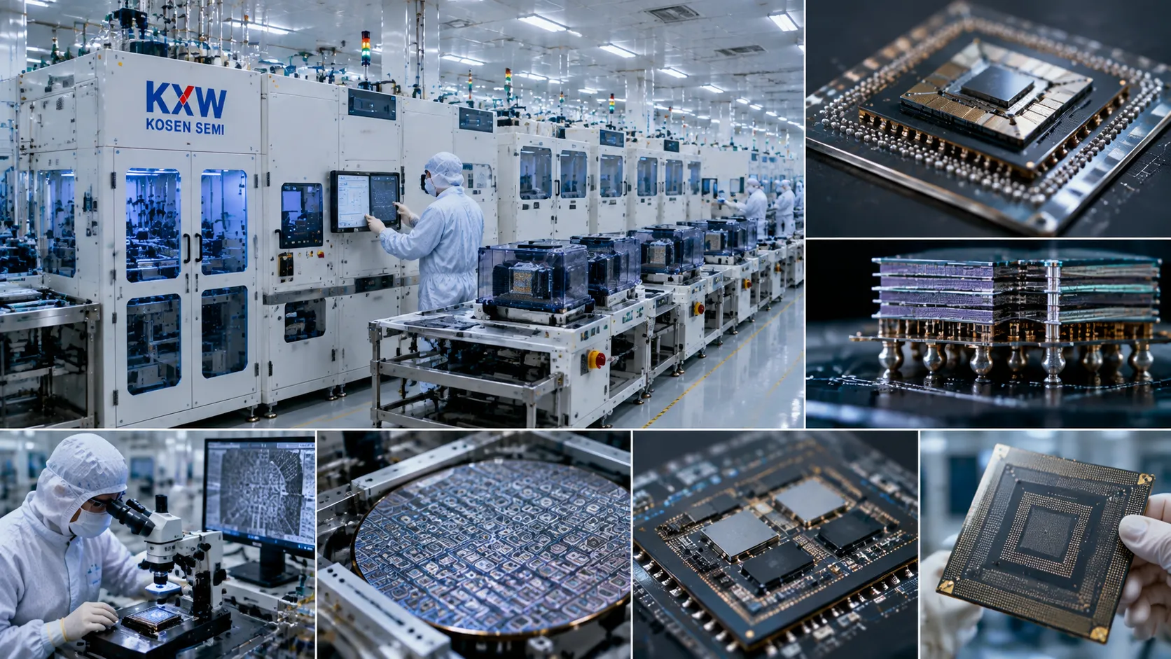
Advanced Semiconductor Packaging Solutions
Modern high-density heterogeneous integration demands thorough residue removal within narrow bump pitches, Through-Silicon Vias (TSVs), and ultra-tight micro-gaps. KOSEN SEMI wet processing equipment leverages targeted megasonic energy and dynamic chemical spraying to eliminate organic flux residues without causing structural damage to sensitive micro-bumps.
- ✓ Flux Removal: Complete clearance of organic flux residues under ultra-tight micro-bump clearances.
- ✓ TSV Wet Processing: Deep trench cleaning with optimized surface tension control for Through-Silicon Vias and high-aspect-ratio features.
- ✓ Micron-Scale Gap Penetration: Custom chemistry delivery forces deep fluid penetration into micro-gaps under 10 microns to prevent bridging defects.
Power Semiconductor Wet Processing Systems
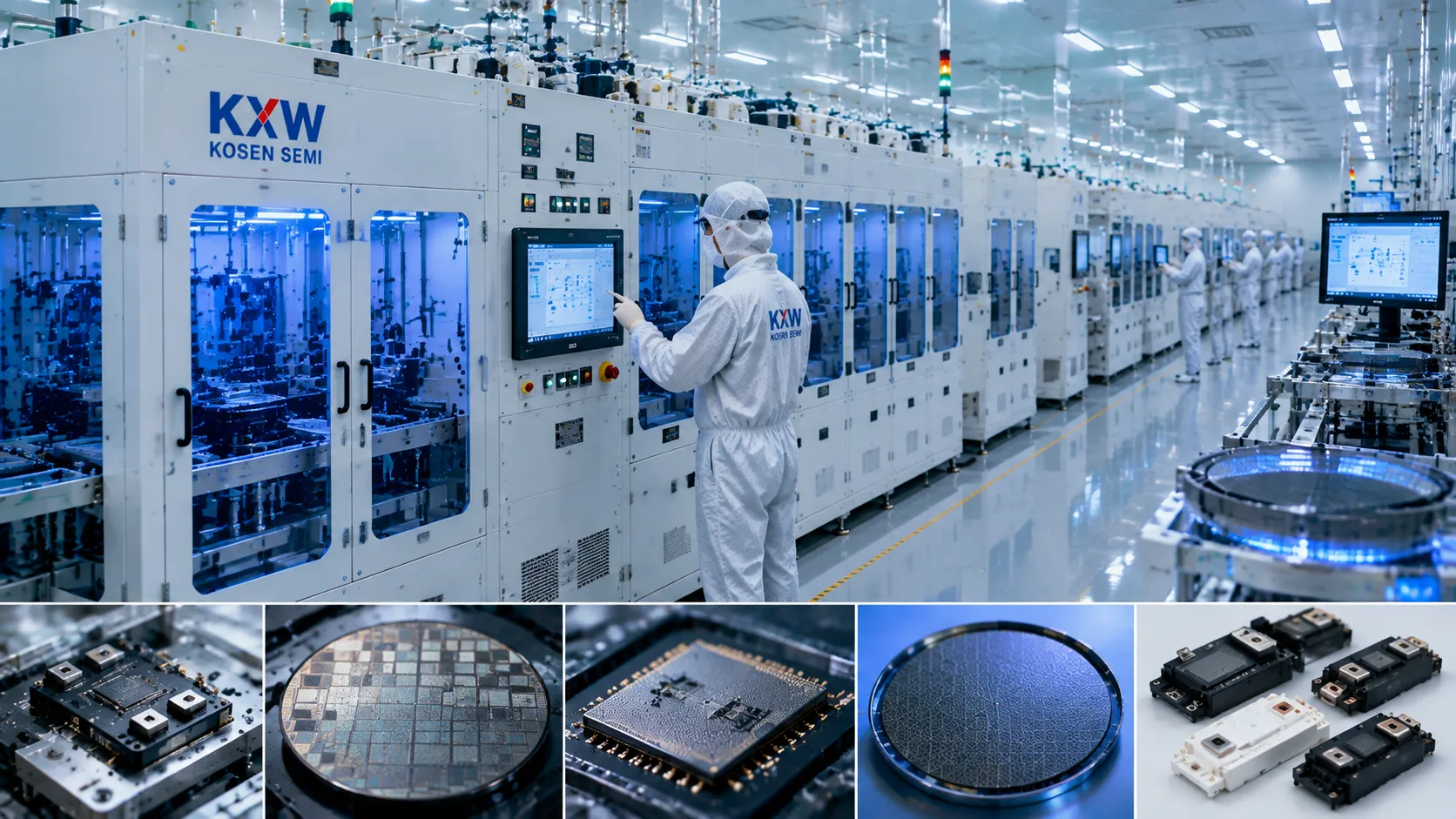
Processing wide-bandgap materials such as Silicon Carbide (SiC) and Gallium Nitride (GaN) presents demanding chemical corrosion and thermal stability challenges. Designed for high-volume power semiconductor production, our high-precision wafer cleaning systems feature corrosion-proof fluid loops engineered to handle high-temperature acid etching and thick photoresist removal safely.
- ✓ High-Temperature Acid Baths: Precise thermal management up to 180°C for fast, uniform substrate etching.
- ✓ Thick Photoresist Stripping: Complete dissolution of heavy polymer layers without substrate or metal layer damage.
- ✓ Controlled Surface Texturing: Controlled chemical etching designed to optimize surface morphology for enhanced electrical performance and adhesion.
MEMS Manufacturing & Release Etching
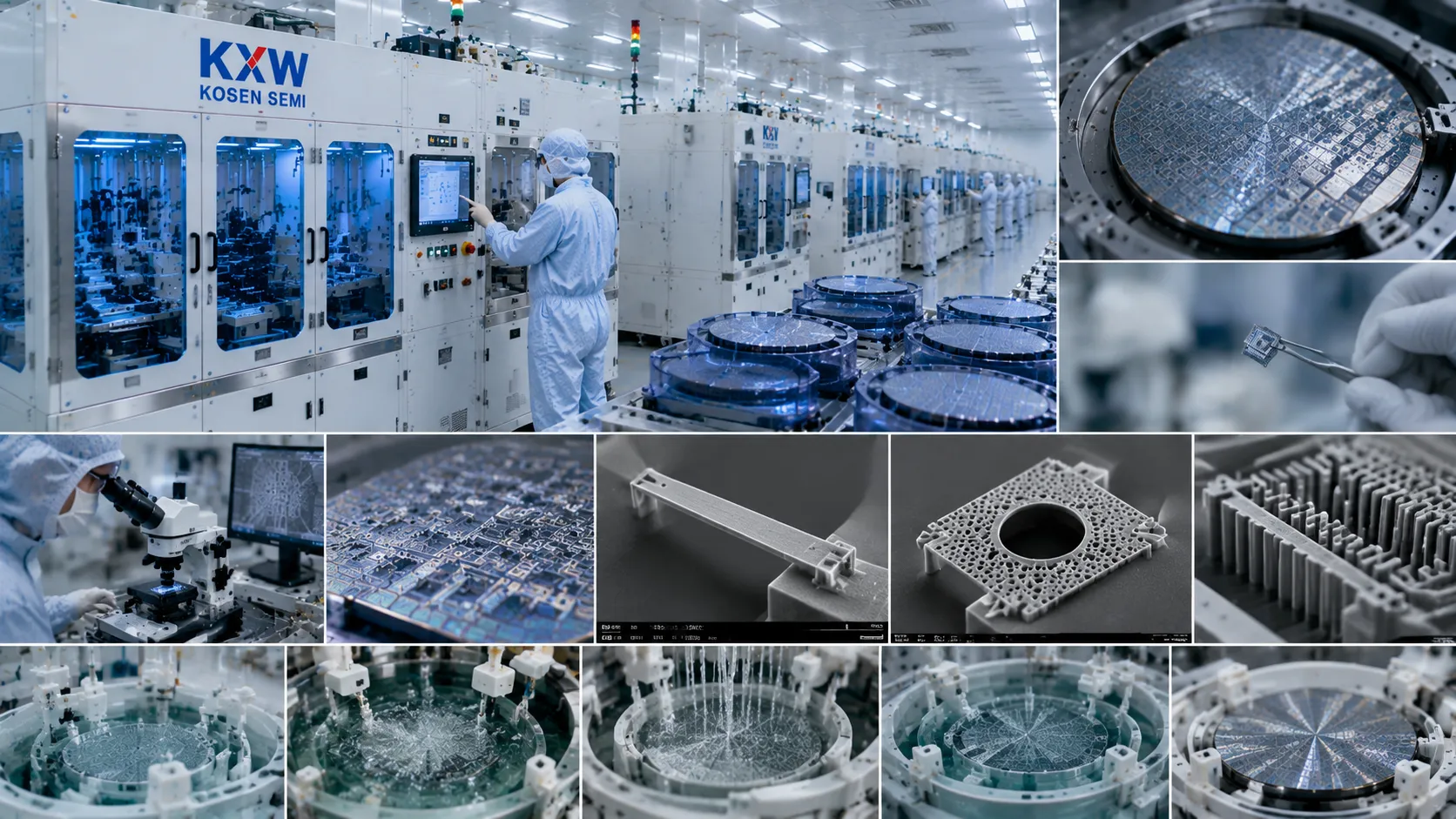
Fabricating delicate MEMS microstructures requires extreme care during liquid processing to prevent stiction and mechanical failure. KOSEN SEMI integrates controlled isotropic etching with advanced surface drying to protect fragile free-standing membranes and micro-actuators, utilizing specialized Single Wafer Cleaning Systems for optimal process stability.
- ✓ Sacrificial Release Etching: Highly selective isotropic etching of oxide and sacrificial layers with minimal structural attack.
- ✓ Megasonic Particle Extraction: Tuned acoustic fields dislodge fine particles without damaging fragile micro-beams.
- ✓ Anti-Stiction Drying: Specialized IPA vapor drying techniques eliminate capillary forces during post-release drying.
Engineered for Complex High-Aspect-Ratio Architectures
KOSEN SEMI delivers customized chemical temperature control, megasonic integration, and advanced fluid agitation to maximize fab yields across all advanced semiconductor packaging and specialty process applications.
Compound Semiconductor & Optoelectronic Applications
High-performance compound semiconductor and optoelectronic devices demand engineered chemical processing, exceptionally high etch selectivity, and stringent surface contamination control. Unlike conventional silicon wafers, III-V materials such as Gallium Arsenide (GaAs), Indium Phosphide (InP), and Gallium Nitride (GaN) feature delicate crystal lattices and high chemical sensitivity. Fabrication line operators require specialized fluid dynamics, precise bath temperature control, and zero-cross-contamination chemical delivery systems to safeguard substrate integrity and maximize die yield.
KOSEN SEMI engineers application-driven wet processing solutions tailored specifically for the specialty semiconductor industry. Integrating isolated chemical circulation manifolds with custom-molded fluoropolymer processing baths, our wet benches and Single Wafer Cleaning Systems ensure chemical purity, uniform boundary layer fluid flow, and reliable yield enhancement across advanced photonics, power devices, and RF integrated circuits.
Pre-Epitaxial Surface Preparation, Selective Etching & Resist Stripping
Fabricating advanced compound semiconductor devices on GaAs, InP, GaN, and SiC substrates demands tight chemical control. Because these specialty materials exhibit high chemical reactivity and fragile crystallographic structures, wet processing tools must control 200 nm-class contaminants, with optimized removal down to 100 nm without inducing lattice pit damage or stoichiometry shifts.
Pre-Epitaxial Surface Cleaning
Removes native oxides, organic residues, and metallic ions down to sub-ppb levels before MOCVD or MBE epitaxial growth, ensuring pristine surface stoichiometry and crystalline film growth without surface pitting.
Selective Chemical Etching
Provides precise isotropic and anisotropic chemical etching with high layer selectivity for III-V heterostructures. Controlled fluid dynamics deliver nanoscale depth uniformity across 2-inch to 8-inch wafers.
Specialized Photoresist Stripping
Utilizes solvent-rated bath circulation and targeted megasonic energy to completely remove thick photoresists and polyimide layers after high-dose ion implantation or metal lift-off, avoiding micro-residues.
Process Specifications & Capabilities
- Supported Substrates: GaAs, InP, GaN, SiC, Sapphire, and InGaAs heterostructures.
- Wafer Sizes: 2-inch to 8-inch substrates and custom thin-wafer carrier configurations.
- Defect Control: Particle control down to 100 nm under optimized conditions and metallic contamination <1E10 atoms/cm².
- Tool Configurations: Automated wet bench systems, semi-automated stations, and single-wafer cleaners.
Precision Wet Cleaning & Etching for Optoelectronics
Manufacturing advanced optoelectronics—including Micro-LED arrays, VCSELs, laser diodes, and photodetectors—demands atomic-level surface smoothness and low-defect device facets. Custom wet processing equipment prevents optical scattering, suppresses non-radiative recombination, and optimizes light extraction efficiency through advanced wafer cleaning systems.
Bevel Etching & Edge Conditioning
Removes edge beads, residual dielectric films, and micro-fractures along wafer margins, significantly reducing particle generation and thermal stress cracking during high-temperature thermal steps.
Controlled Surface Polishing
Achieves sub-nanometer RMS surface roughness on optical emission facets and sensor active areas, maximizing light transmission and internal quantum efficiency (IQE) for photonics.
Post-Dicing Micro-Particle Cleaning
Combines megasonic agitation with specialized chemistry to dislodge dicing slurry and 200 nm-class debris from high-density Micro-LED pixel arrays without lifting fragile micro-structures.
Optoelectronic Process Features
- Target Devices: Micro-LED / Mini-LED arrays, VCSELs, edge-emitting laser diodes, and PIN photodetectors.
- Substrate Handling: Ultra-thin wafers (<100 µm), sapphire carriers, and fragile glass substrates.
- Facet Integrity: Contact-free liquid processing on active optical emission facets.
- Chemical Management: Continuous closed-loop recirculation with inline concentration monitoring.
Hardware Engineering & Process Control for Specialty Semiconductors
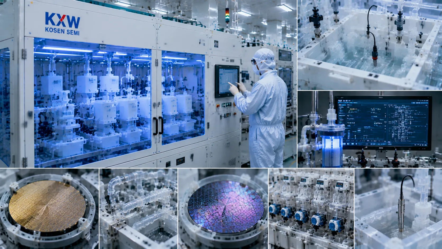
Processing aggressive etching chemistries and sensitive non-silicon substrates requires specialized hardware engineering and precise fluidic control. Leveraging our advanced Engineering Capability, KOSEN SEMI utilizes custom-molded fluoropolymer tanks, isolated chemical distribution paths, and precision thermal management systems to ensure reproducible processing across specialty semiconductor manufacturing lines.
Corrosion-Proof Bath Materials
Built with ultra-high purity PFA, PTFE, and seamless molded PVDF tanks engineered to withstand concentrated acids, hot organic solvents, and fluorine-based etchants without ionic leaching or degradation.
Cross-Contamination Prevention Chemistry Isolation
Fully isolated fluidic lines, dedicated chemical delivery manifolds, and active exhaust segregation eliminate chemical cross-talk between etching, resist stripping, and final DI water rinsing modules.
Precise Temperature Regulation
In-line chemical heaters and fluoropolymer heat exchangers deliver precise closed-loop temperature control within ±0.1°C, guaranteeing stable chemical etch rates and process repeatability.
KOSEN SEMI Process Assurance
Custom fluoropolymer bath architectures and precise thermal control engineered for III-V compound semiconductor and photonics manufacturing.
Wet Process Equipment Type vs. Application Matrix
Map key downstream process requirements directly to high-performance hardware. KOSEN SEMI delivers manual wet stations, semi-automated tools, and fully automated wet bench systems to accommodate diverse production scales and maintain stringent process control standards across every wafer fabrication phase.
| Tool Categories | Front-End Fab | Advanced Packaging | Compound Semi |
|---|---|---|---|
| Automated Wet Bench High-throughput batch wafer cleaning equipment & immersion etching | Optimal Fit FEOL/BEOL cleaning & precision oxide etching | Supported Substrate prep & bulk photoresist removal | Optimal Fit GaN/SiC wafer cleaning & controlled chemical etching |
| Single-Wafer Cleaner Ultra-clean Single Wafer Cleaning Systems chemical processing & acoustic rinse | Optimal Fit 200 nm particle control, optimized to 100 nm, with controlled cross-contamination | High Precision Post-dicing clean & micro-bump residue removal | Supported Fragile substrate single-sided surface treatment |
| Single-Wafer Scrubber Non-contact atomized spray & soft brush particle removal | Standard Wafer backside cleaning & post-CMP slurry removal | Optimal Fit Post-grinding particle removal & tape residue scrubbing | High Precision Polishing compound removal for SiC & GaN wafers |
| Chemical Stripper High-efficiency solvent & temperature-controlled acid photoresist removal | Supported High-dose implant resist strip & post-ash residue cleaning | Optimal Fit Thick photoresist stripping & 3D structure lift-off | Optimal Fit Metal lift-off & solvent-based immersion stripping |
Flexible Equipment Architectures for Every Production Scale
Select the ideal tool architecture matched to your target yield rates, process nodes, and factory automation standards backed by our advanced Engineering Capability.
Manual Wet Stations
Ideal for R&D laboratories, pilot lines, and specialized low-volume production.
Semi-Automated Systems
Combines precise recipe-driven process control with flexible, operator-assisted substrate handling.
Automated Wet Benches
Fully automated wet bench systems engineered for high-volume manufacturing with robotic transfer.
Advanced Wafer Cleaning Equipment & Process Control
Engineered with micro-dosing precision, thermal uniformity, and real-time bath concentration monitoring to optimize yield stability.
Verified Fab Performance, SEMI Compliance & Yield Rate Enhancement
KOSEN SEMI delivers high-yield semiconductor wet processing equipment engineered specifically for high-volume manufacturing fabs. Through strict cleanroom compliance, 200 nm-class contamination control, optimized down to 100 nm, and international SEMI safety certifications, our automated wafer cleaning systems protect substrate integrity and drive measurable yield rate enhancement across active production lines.
Strict airborne contamination control prevents micro-particle fallout during ultra-clean surface preparation.
Full compliance with global environmental, chemical isolation, electrical, and ergonomic design guidelines.
Ultra-pure chemical fluid paths limit surface metallic impurities on critical front-end silicon wafers.
Demonstrated line yield rate enhancement achieved in active 200mm volume wafer fabrication facilities.
8-Inch Wafer Fab Defect Elimination Benchmark
A high-volume 200mm integrated circuit manufacturer implemented KOSEN SEMI single wafer cleaning systems to control fine particulate particle bottlenecks during pre-gate oxide surface preparation cycles.
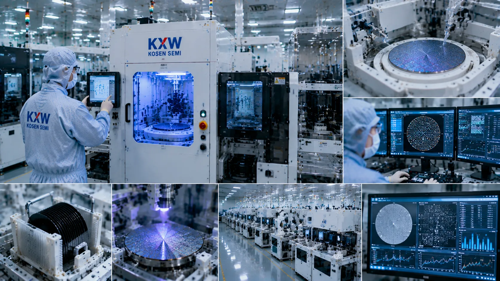
Optimized fluid dynamics and multi-frequency megasonic agitation successfully removed contaminants at the 200 nm production scale, with optimized capability down to 100 nm.
Stabilized chemical bath uniformities prevented particle re-deposition, significantly reducing scrap rates across active wafer lots.
International SEMI Standards & Host Automation
All KOSEN SEMI wet processing systems pass comprehensive Factory Acceptance Testing (FAT) and rigorous site qualification protocols (IQ/OQ/PQ) backed by our advanced engineering capability to maintain strict cleanroom compliance and meet demanding semiconductor industry specifications.
Engineered in full accordance with SEMI S2, S8, and S14 guidelines for safe chemical isolation, real-time exhaust monitoring, and ergonomic operator access.
Fully compliant with SEMI E30, E37, and E4/E5 protocols, enabling real-time process monitoring, automated recipe selection, and fab-wide data logging.
Constructed exclusively with high-purity PFA, PTFE, and PVDF components to guarantee zero metallic ion leaching and maximum chemical durability.
Comprehensive Fab Application Support
Dedicated operational guarantees designed to maintain 99.8% equipment availability across global manufacturing facilities.
24/7 Expert Application Support
Direct operational access to senior process engineers for continuous chemical bath analysis, recipe refinement, and rapid technical resolution.
Localized Spare Parts Logistics
Strategic regional hubs ensure rapid dispatch of critical high-purity valves, pumps, sensors, and fluid assemblies to eliminate unscheduled downtime.
Smart Automation & Data Integration
Seamless interface compatibility with smart factory automation systems facilitates predictive maintenance alerts and comprehensive batch traceability.
Semiconductor Wet Application FAQs
Find authoritative technical answers regarding wet bench integration, custom wet processing, 200 nm-class defect reduction, and seamless pilot-to-production scalability.
How does KOSEN SEMI ensure precise semiconductor equipment fit across specific wafer sizes and technical nodes?
Establishing optimal semiconductor equipment fit requires a comprehensive baseline audit of wafer dimensions, chemical compatibility, throughput expectations, and target defect density limits. KOSEN SEMI process engineering specialists evaluate fab floor constraints across 150mm, 200mm, and 300mm wafer formats to specify the ideal system architecture.
- Automated Wet Bench Systems: Preferred for high-volume immersion processing, mature nodes, and compound semiconductor applications requiring multi-tank chemical sequences and continuous batch processing.
- Single-Wafer Cleaning Tools: Engineered for 200 nm-class IC fabrication, with optimized capability down to 100 nm where airborne molecular contamination (AMC), cross-contamination prevention, and localized megasonic cleaning are critical.
- Process Control Integration: All configurations feature real-time chemical dosing, inline temperature regulation (±0.5°C), and full SECS/GEM interface compatibility for automated fab management.
By evaluating chemical bath recirculation rates, particle filtration targets, and robotic handling precision, KOSEN SEMI delivers custom wet processing setups tailored to your specific wafer fabrication requirements. Learn more about our robust engineering capability to see how we build customized solutions for unique process demands.
Can chemical tank geometries and fluid delivery be customized for non-standard compound substrates or MEMS?
Yes. Non-standard compound substrates—including GaAs, GaN, InP, and SiC—along with fragile MEMS structures require specialized fluid mechanics and material resistance that off-the-shelf systems cannot provide. KOSEN SEMI excels at custom wet processing solutions, engineering dedicated chemical vessels and fluid delivery loops tailored to aggressive chemistries and sensitive surface topographies.
Custom-molded PTFE, PFA, and high-purity quartz baths eliminate elemental leaching and withstand extreme acid or solvent processing temperatures.
Engineered bath circulation eliminates stagnant boundary layers, ensuring uniform chemical exchange and consistent etch rates across non-standard wafer geometries.
Whether implementing high-temperature acid etching, localized megasonic agitation, or anti-stiction drying for MEMS sacrificial layer releases, our process engineering team custom-builds fluid delivery systems to match exact fab requirements.
What methods prevent cavitation damage and chemical trapping during micro-gap cleaning in advanced packaging?
Advanced packaging architectures—such as 2.5D/3D integration, Chiplet structures, Through-Silicon Vias (TSVs), and fine-pitch micro-bumps—create extremely tight gaps where surface tension prevents standard cleaning fluids from penetrating. Additionally, uncalibrated acoustic cleaning can cause mechanical cavitation damage to fragile interconnects.
KOSEN SEMI mitigates these risks through a combination of proprietary acoustic energy controls, precise chemical dynamics, and surface tension management:
- Synchronized Multi-Frequency Megasonics: Uniformly distributes acoustic energy to dislodge flux residues and 200 nm-class particles without inducing destructive cavitation pitting on delicate micro-bumps.
- Low-Surface-Tension Chemical Formulations: Enhanced wetting agents lower contact angles, allowing wet cleaning solutions to fully permeate micro-gaps under 10 microns.
- Surface Tension Gradient (STG) & IPA Vapor Drying: Replaces residual liquid in deep trenches with isopropyl alcohol vapor, completely eliminating water marks, chemical trapping, and structural stiction.
How do your tools support seamless process scaling from pilot R&D lines to full mass production?
Transitioning a semiconductor wet process recipe from pilot R&D to high-volume manufacturing (HVM) requires total chemical kinetic parity and identical boundary conditions. KOSEN SEMI builds modular wet processing hardware that utilizes identical tank materials, fluid delivery dynamics, sensor suites, and control logic across manual wet stations, semi-automated systems, and fully automated wet benches.
Recipe parameters established during R&D—including bath temperature profiles, megasonic power densities, chemical dispense rates, and spin-dry parameters—can be transferred directly to continuous production tools without re-qualifying fundamental process windows or compromising semiconductor equipment fit.
To eliminate technical risk prior to capital investment, KOSEN SEMI provides pre-purchase process evaluations and sample testing (demo runs) in our cleanroom facilities. Fab engineering teams can test target wafers, verify particle reduction rates, and optimize yield parameters prior to equipment deployment.
Ready to Optimize Your Semiconductor Wet Processing Yield?
Whether constructing a new fab line or upgrading existing wet processing equipment, KOSEN SEMI provides expert process consultation to match your exact cleaning, etching, and surface preparation requirements. Discover how our Engineering Capability drives innovation.
Contact KOSEN SEMI today to initiate a customized application assessment, request a demo run on our Automatic Wet Bench Systems , or receive a dedicated equipment proposal.