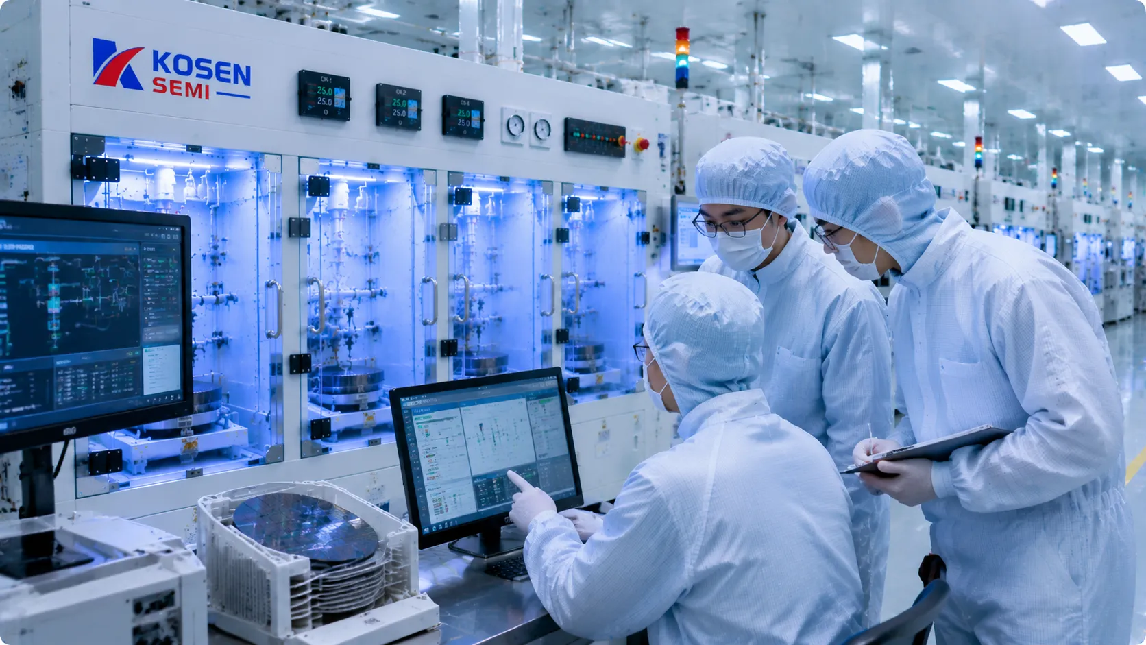
End-to-End Wet Processing Equipment Integration
Our wet processing equipment comprehensively covers core semiconductor manufacturing steps, ensuring high purity and stability at every stage. From initial substrate preparation to final interconnect packaging, KOSEN SEMI line-matched architectures eliminate micro-contamination bottlenecks and streamline complex semiconductor manufacturing workflows for mature-node and specialty semiconductor production. Learn more about our focus / about-us core mission and technical expertise.
Front-End Substrate Cleaning & Precision Etching Operations
Front End of Line (FEOL) manufacturing demands uncompromising surface cleanliness to prevent critical defect modes during transistor gate formation. KOSEN SEMI wet processing systems combine advanced chemical delivery, megasonic agitation, and ultra-clean IPA Marangoni drying techniques to achieve a high-yield wafer cleaning process for stable process control at 200 nm nodes, with selected applications supportable down to 100 nm.
Core FEOL Process Deliverables
- ✓ Controlled Particle Removal: Megasonic-assisted wet processing supports application-specific particle reduction for 200 nm production, with process evaluation available for requirements down to 100 nm.
- ✓ Organic Residue Stripping: High-temperature SPM chemical baths deliver complete photoresist removal and precise surface oxidation control.
- ✓ Precision Oxide Etching: Dilute HF etching modules provide controlled oxide etching uniformity across supported wafer sizes and process recipes.
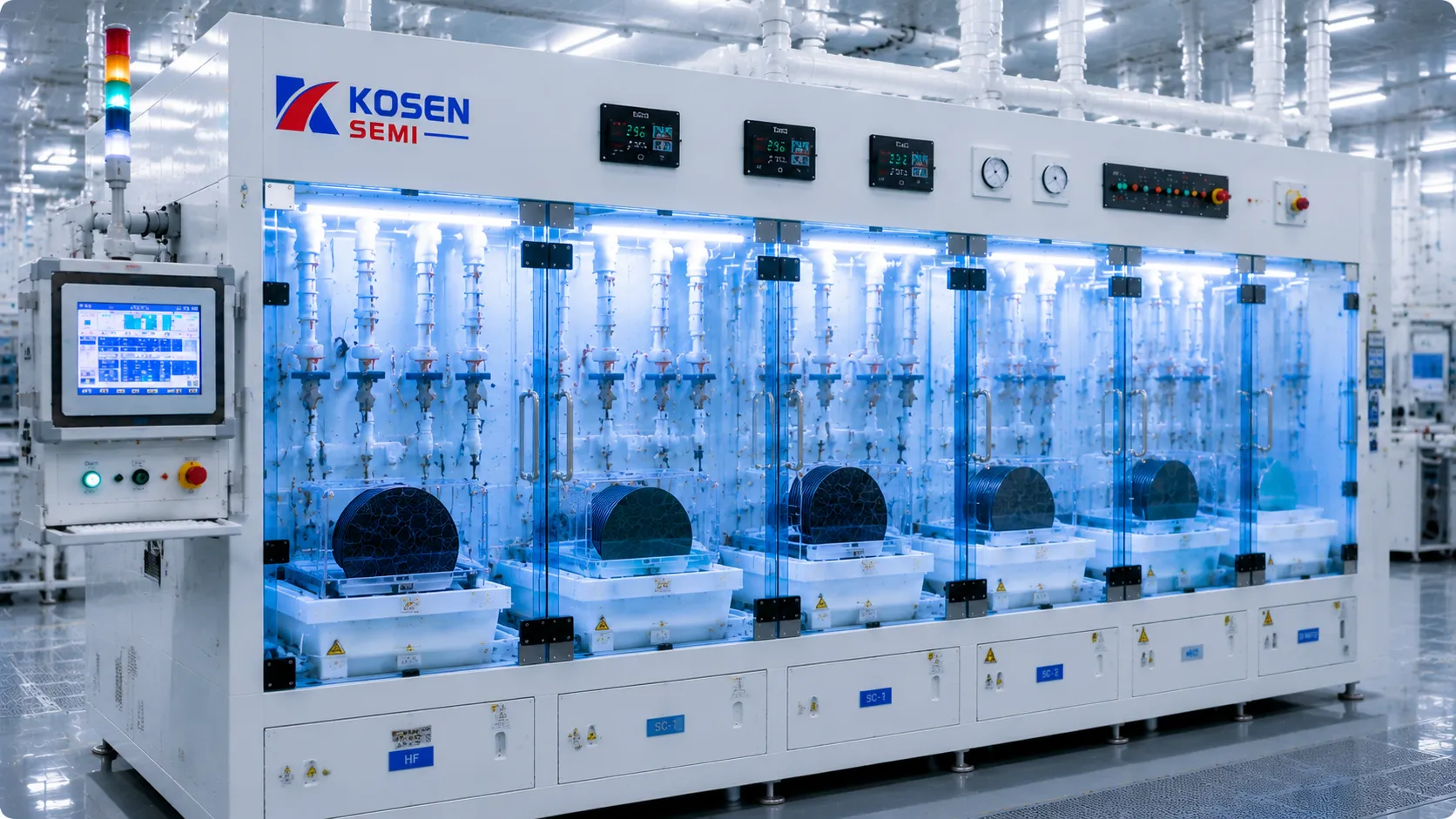
Equipment Alignment Specs
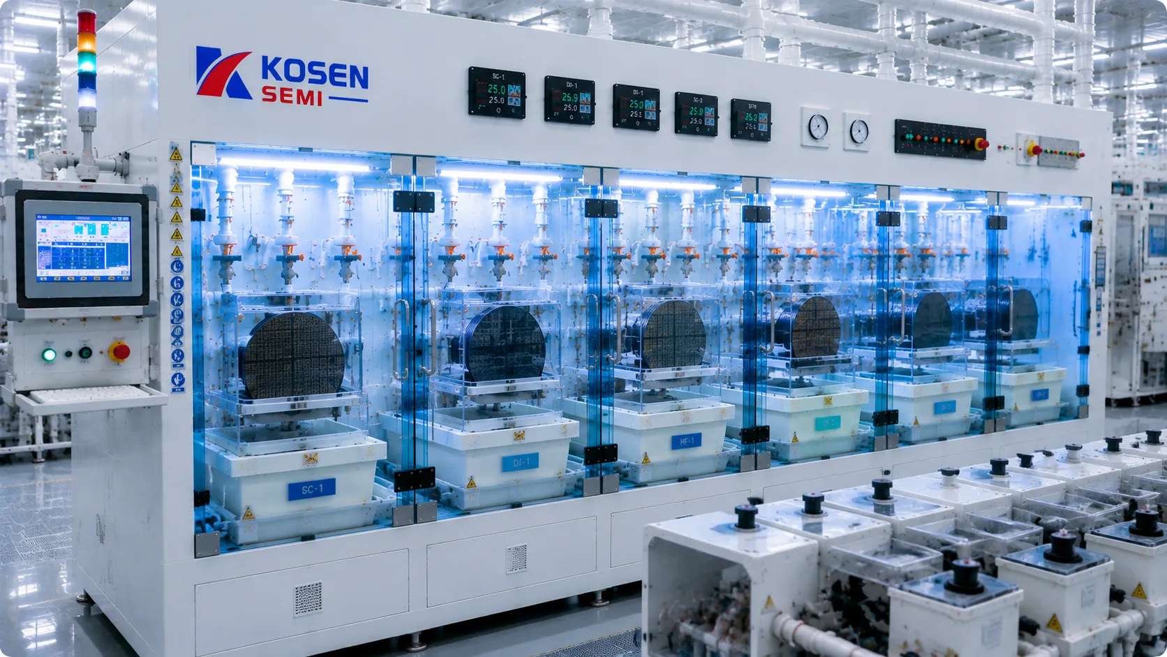
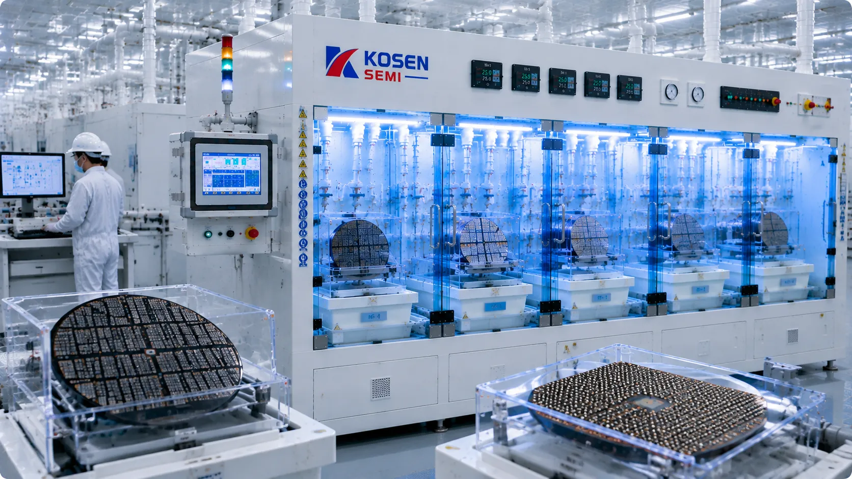
Workflow Process & Equipment Alignment Matrix
Matching semiconductor manufacturing workflows with target-specific wet processing equipment ensures maximum tool utilization, lower cost of ownership, and consistently higher wafer yield across fab operations.
| Fabrication Node | Key Wet Operation | Primary Contaminant Target | Recommended Tool Type | Yield Impact |
|---|---|---|---|---|
| FEOL Substrate Cleaning | RCA Clean & Megasonic SPM | Particles, Organics, Trace Metals | Automated Batch Wet Bench / Single Wafer | Eliminates Fatal Substrate Defects |
| FEOL Gate Patterning | Dilute HF Etch & Clean | Native Oxides & Etch Polymers | Precision Single-Wafer Platform | 200 nm Threshold Control, Optimized to 100 nm |
| BEOL Interconnect | Post-CMP Slurry & Solvent Strip | Abrasive Slurry & Metallic Residues | Single-Wafer Chemical Clean Tool | Prevents Interconnect Leakage Current |
| Advanced Packaging | TSV Trench & Micro-Bump Clean | Trench Residues & Flux Contaminants | High-Aspect-Ratio Bench System | Ensures High Interconnect Reliability |
Precision Contamination Control & Yield Management
Mature-node semiconductor fabrication requires stable contamination control across every wet process step. As device architectures grow increasingly dense and feature geometries shrink, microscopic defect particles, metallic trace impurities, and organic residues become the primary drivers of yield loss. KOSEN SEMI delivers high-purity contamination removal platforms and automated chemical delivery systems engineered to satisfy the most rigorous wafer cleanliness standards in modern semiconductor manufacturing.
Powered by proprietary fluid dynamics and real-time process monitoring, our wet processing solutions resolve critical line bottlenecks to maximize total fab productivity. By combining high-precision chemical dosing with advanced physical agitation, KOSEN SEMI equipment protects fragile surface topographies while eliminating nanoscale defects to drive continuous engineering capability and yield optimization.
Particle Control for Mature Nodes
Engineered specifically for critical defect reduction during advanced wafer cleaning systems and etching workflows. Advanced physical and chemical removal mechanisms eliminate microscopic surface contaminants without damaging fragile high-aspect-ratio patterns.
- • Application-Specific Particle Reduction: Cleaning recipes are optimized to protect yield in 200 nm production, with selected processes evaluated down to 100 nm.
- • Uniform Megasonic Energy: Precise acoustic energy distribution prevents localized pattern damage.
- • Zero Boundary Damage: Gentle micro-fluidic agitation preserves delicate circuit features.
Precision Chemical Delivery
Automated closed-loop chemical dosing systems engineered to reduce raw chemical consumption by up to 30% while maintaining absolute bath stability across extended manufacturing campaigns. Integrate with our specialized Single Wafer Cleaning Systems for optimal cleanliness.
- • 30% Chemical Savings: Smart dosing and recirculation lower overall operational cost per wafer.
- • Real-Time Spiking: Closed-loop sensors maintain stable bath concentration control within the validated recipe window.
- • Thermal Uniformity: Continuous recirculation guarantees process fluid temperature stability.
Automated Fab Integration
Purpose-built for 24/7 high-throughput production with seamless Automated Material Handling System (AMHS) compatibility. Standardized SECS/GEM communication protocols ensure instant host system synchronization.
- • 24/7 Operational Uptime: High equipment availability designed for continuous, high-volume fabs.
- • SECS/GEM Compliance: Full software integration with factory host systems and MES.
- • Predictive Maintenance: Integrated sensor networks track component wear to prevent downtime.
Advanced Micro-Contamination Reduction Capabilities
Maximizing die yield in modern semiconductor fabs depends on controlling non-visual defects, trace metallic impurities, and organic residues. KOSEN SEMI integrates optimized fluid dynamics with multi-frequency acoustic fields to strip surface micro-contaminants without etching delicate substrate layers.
Our automated chemical delivery systems utilize ultra-high-purity PFA circulation loops, continuous sub-micron filtration, and inline concentration monitoring. By eliminating chemical degradation and re-contamination, our platforms deliver consistent, repeatable process results across extended manufacturing campaigns.
| Performance Metric | Industry Baseline | KOSEN SEMI Advantage |
|---|---|---|
| Particle Removal Threshold | Particle size ≥ 200 nm, with optimized evaluation down to 100 nm | Process-specific particle control |
| Chemical Consumption Rate | Standard baseline consumption | Up to 30% reduction via closed-loop dosing |
| Chemical Bath Stability | ±0.5% concentration variance | Closed-loop concentration control |
| Fab Automation Interface | Manual or semi-automated options | Full SECS/GEM & AMHS fab automation |
| Yield Optimization Impact | Standard baseline process yield | Up to 15%+ overall yield improvement |
Precision Dosing Technology
Automated chemical delivery systems eliminate batch variance by continuously monitoring fluid refractive index, electrical conductivity, and bath temperature in real time.
Proactive Yield Protection
Integrated defect logging and real-time sensor analytics empower process engineers to identify and isolate micro-contamination trends before they affect entire wafer lots.
Matching Semiconductor Equipment Form Factors to Application Scenarios
KOSEN SEMI offers versatile wet processing equipment portfolios from single-wafer to batch immersion processing, flexibly satisfying requirements across diverse production lines. Evaluate process compatibility and select optimal wet bench systems to maximize yield and factory throughput. Learn more about our technical foundations on our about-us page.
Batch Wet Bench Processing Fit
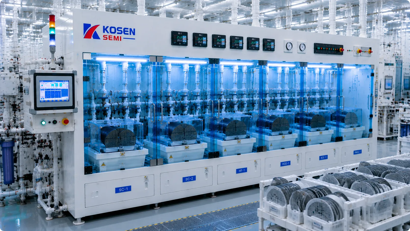
Batch processing delivers maximum wafer throughput and lowest cost of ownership (CoO) for bulk chemical etching, stripping, and wafer cleaning in high-volume fabs. Designed for continuous multi-wafer immersion with ultra-low chemical consumption per unit.
- Mass Wafer Immersion: Simultaneous high-uniformity processing of 25 to 50 wafers.
- High Chemical Efficiency: Recirculated chemical bath architecture lowers operational costs.
- Target Applications: Bulk oxide removal, nitride etching, RCA clean, and PR stripping within dedicated wafer-cleaning-systems.
Semiconductor Equipment Fit
Best suited for 200mm and 300mm mature node foundries requiring stable batch throughput.
Single-Wafer Processing Platform Fit
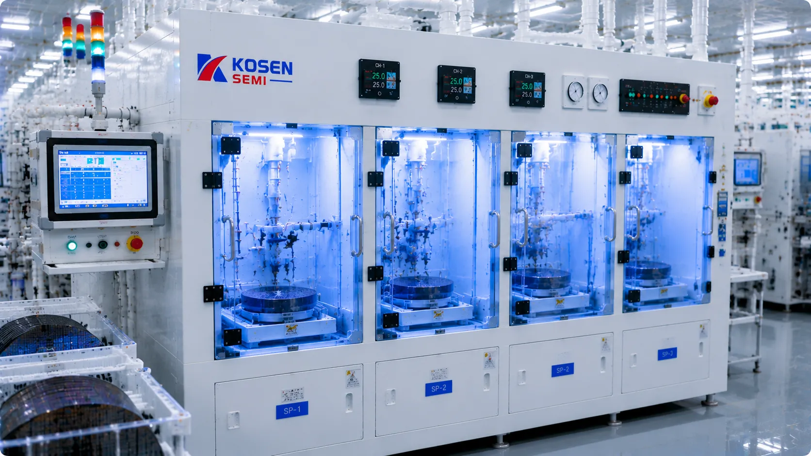
Single-wafer processing platforms offer extreme chemical isolation and defect control for advanced semiconductor manufacturing nodes. Prevents cross-contamination with precise spin-cleaning and targeted point-of-use spray dispense chemistry.
- 100 nm Process Support: Selected recipes can be evaluated for demanding mature-node applications.
- Rapid Recipe Switching: Chamber versatility for multi-product and flexible development lines.
- Target Applications: Post-etch residue clean, FEOL critical clean, and bevel etching deployed on our customized Single Wafer Cleaning Systems.
Process Compatibility Focus
Optimized for advanced 300mm logic, DRAM, and 3D NAND manufacturing demanding zero cross-contamination.
Process Compatibility & Technical Specification Matrix
Direct comparison of wet equipment architecture capabilities to simplify preliminary tool selection.
| Selection Criteria | Batch Wet Bench Systems | Single-Wafer Platforms |
|---|---|---|
| Primary Strength | Maximum Throughput & Lowest CoO | Extreme Process Isolation & Defect Control |
| Target Fabrication Environment | High-Volume Mass Production | High-Mix & Specialty Fabs |
| Defect Control Threshold | Standard Particle Density Targets | Application-Specific Particle Control |
| Chemical Dispense Mode | Recirculated & Filtered Mass Baths | Point-of-Use Single-Pass Dispense |
| Footprint Efficiency | High WPH Output per Square Meter | Modular Multi-Chamber Scalability |
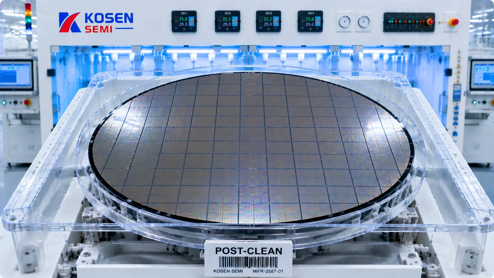
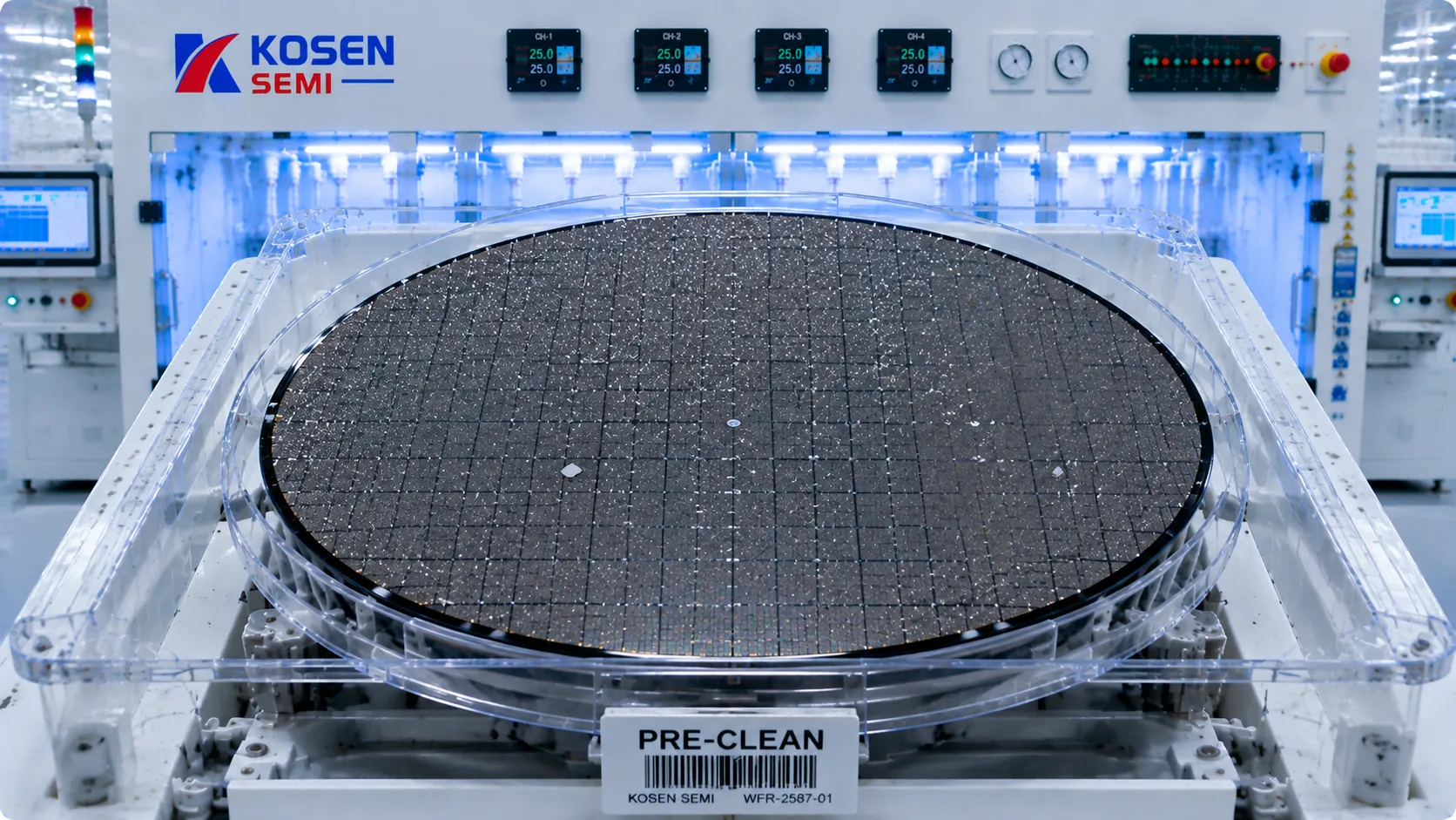
Wafer Surface Cleanliness Comparison
Drag the inspection line to compare wafer surface conditions before and after KOSEN SEMI wet cleaning process.
Certifications and Trust Signals
KOSEN SEMI wet processing systems are engineered for controlled clean manufacturing and customer-site safety requirements. Supported by documented quality controls, project-specific specifications, and customer acceptance procedures, our equipment empowers procurement teams and process engineers to specify solutions with complete confidence while learning more about-us and our commitment to building long-term trust.
Why Compliance Credentials Matter in Semiconductor Manufacturing
In modern semiconductor manufacturing, maintaining uncompromised quality and cleanroom compliance is paramount. Semiconductor fabs operate under ultra-strict contamination budgets where even trace impurities can cause yield-killing defects across an entire wafer lot. Selecting equipment with verified ISO cleanroom compliance and complete SEMI safety certification mitigates qualification risks and significantly compresses Tool Acceptance Testing (TAT) schedules. Engineered for mature-node and specialty-process requirements, KOSEN SEMI wet processing systems deliver audit-ready compliance for demanding foundry environments, fully integrated into our flagship semiconductor-wet-bench-systems.
Our operational foundation is backed by an ISO 9001 quality management system, ensuring full component traceability, standardized manufacturing workflows, and rigorous revision control across every tool line. Equipment assembly is performed in a controlled environment aligned with ISO 14644-1 Class 5–7, with system compliance configured according to customer requirements and applicable SEMI S2 (Environmental, Health, and Safety) and SEMI S8 (Ergonomic) guidelines, KOSEN SEMI tools, including our advanced Automatic Wet Bench Systems, seamlessly integrate into tier-1 fabs without requiring costly facility re-engineering or delayed safety clearances.
International Standards and Certifications
ISO 9001:2015
Certified quality management system governing design, precision manufacturing, and lifecycle field support. Ensures stringent process traceability and tool-to-tool matching.
ISO 14644-1 Class 5–7
Clean assembly environment aligned with ISO Class 5–7. Customer-site installation requirements are confirmed for each project.
SEMI S2 & SEMI S8
Full adherence to SEMI S2 safety standards and SEMI S8 ergonomic design principles, streamlining environmental health and safety (EHS) audits across global fabs.
Global Market Approvals
Comprehensive CE marking and regional electrical safety compliance enable frictionless equipment delivery and commissioning across North American, European, and Asian fabs.
Proven Results at Tier-1 Semiconductor Fabs
KOSEN SEMI wet processing equipment has been rigorously qualified across high-volume logic, memory, and compound semiconductor foundries globally. Real-world performance data highlights our contribution to semiconductor yield management and operational efficiency.
Chemical Consumption Reduction
Advanced chemical delivery and automated recirculation technology reduce expensive HF and SC1 usage by up to 30%, optimizing Cost of Ownership (CoO) while maintaining pristine surface cleanliness.
Defect Density Control
Post-clean defect density consistently performs below baseline process-of-record (POR) limits, accelerating advanced gate-all-around (GAA) and FinFET yield ramp cycles.
Continuous Uptime Operation
Delivering Mean Time Between Failures (MTBF) exceeding 2,000 hours, integrated SECS/GEM real-time telemetry reduces unscheduled downtime and elevates fab productivity.
Compliance Coverage at a Glance
The table below outlines the key international standards governing KOSEN SEMI equipment, detailing certification scope, compliance status, and direct operational benefits for semiconductor fab operators.
| Standard | Scope | Compliance Level | Fab Benefit |
|---|---|---|---|
| ISO 9001:2015 | Quality management system — end-to-end design through service | Certified | Guarantees traceable supply chain and strict tool-to-tool process repeatability |
| ISO 14644-1 Class 5–7 | Airborne particulate and cleanroom cleanliness classification | Compliant | Supports project-specific integration into mature-node and specialty fabs |
| SEMI S2 | Environmental, health, and safety performance for semiconductor equipment | Full Compliance | Speeds up EHS sign-offs and eliminates regulatory bottlenecks during tool commissioning |
| SEMI S8 | Ergonomic design criteria for semiconductor manufacturing equipment | Full Compliance | Enhances operator safety, reduces ergonomic risk, and simplifies workplace safety audits |
| SECS/GEM | Standardized host-to-equipment communications protocol | Native Support | Facilitates plug-and-play AMHS automation and real-time process monitoring |
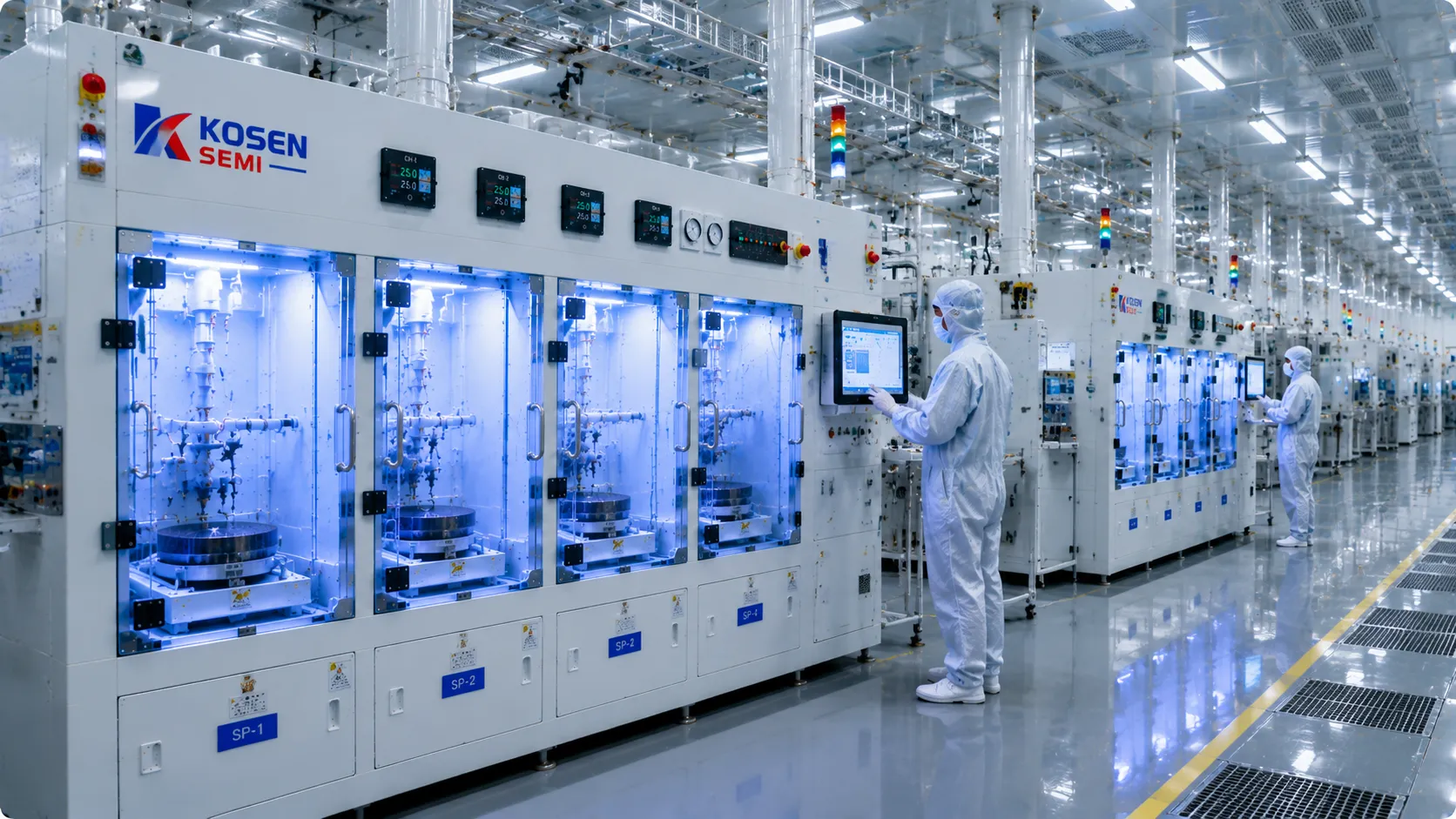
Adopted by Leading Global Semiconductor Fabs
Strictly adhering to SEMI international manufacturing standards, KOSEN SEMI equipment has been adopted by multiple leading global semiconductor wafer fabs. Our robust equipment architecture supports high-volume manufacturing across logic, 3D NAND, DRAM, and compound semiconductor facilities worldwide.
Every tool deployment is accompanied by specialized process application engineers who manage tool qualification, process of record (POR) matching, and continuous yield management. This end-to-end support model ensures our strict compliance credentials translate into tangible operational efficiency and superior chip output.
- 100% Audit Readiness: Comprehensive compliance documentation packages for rapid tool acceptance testing (TAT) and EHS clearance.
- Seamless AMHS Integration: Native SECS/GEM protocol compatibility enables automated material handling and real-time tracking.
- Global Service Support: On-site field application engineers dedicated to continuous yield optimization and process reliability.
Semiconductor Wet Processing FAQ
In-depth answers for fab planning teams, process engineers, and facility managers evaluating cleanroom equipment fit, integration timelines, and semiconductor equipment ROI. KOSEN SEMI delivers end-to-end technical support—from early-stage process validation through long-term high-volume manufacturing. Learn more about our company mission on our about-us page.
AMHS, SECS/GEM, and Factory Automation Integration
KOSEN SEMI wet processing platforms feature native SECS/GEM (SEMI E5/E30) communication protocols, facilitating seamless automated handshakes with fab-level Manufacturing Execution Systems (MES) and Automated Material Handling Systems (AMHS) without requiring proprietary third-party middleware.
- SECS-II / GEM & HSMS compliance: Fully compliant with SEMI E5, E30, and E37 (HSMS) standards for real-time lot tracking, recipe execution, automated parameter downloading, and fault diagnostics.
- AMHS & OHT interface compatibility: Engineered to SEMI E15.1 and E47.1 standards, supporting 200 mm and 300 mm FOUP/FOSB load ports with active carrier clamping and optical placement sensors.
- Host & CIM layer connectivity: Supports open OPC-UA, TCP/IP, and Modbus communications for effortless integration with leading CIM systems including Siemens Opcenter and Applied Materials APF.
- Advanced recipe interlocks: Hardware- and software-level interlocks ensure automatic recipe verification, preventing misprocessing and cross-contamination before wafer handling begins.
Pre-shipment Factory Automation (FA) simulation testing at KOSEN SEMI ensures turnkey integration on site, minimizing tool hookup time and accelerating fab qualification milestones.