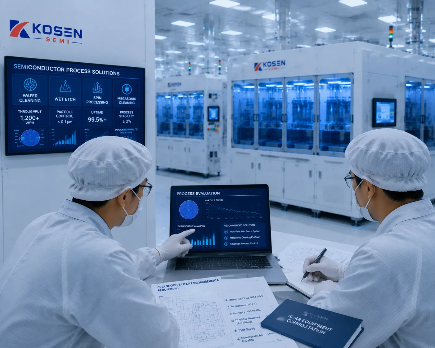
Advanced IC Manufacturing Equipment & Ultra-Clean Processing Solutions
Empowering global semiconductor fabs with controlled chemical processing, high-uniformity wet etching, and controlled microcontamination management for 200 nm processes for maximum IC yield. Discover our company's core focus and values on our about-us page.
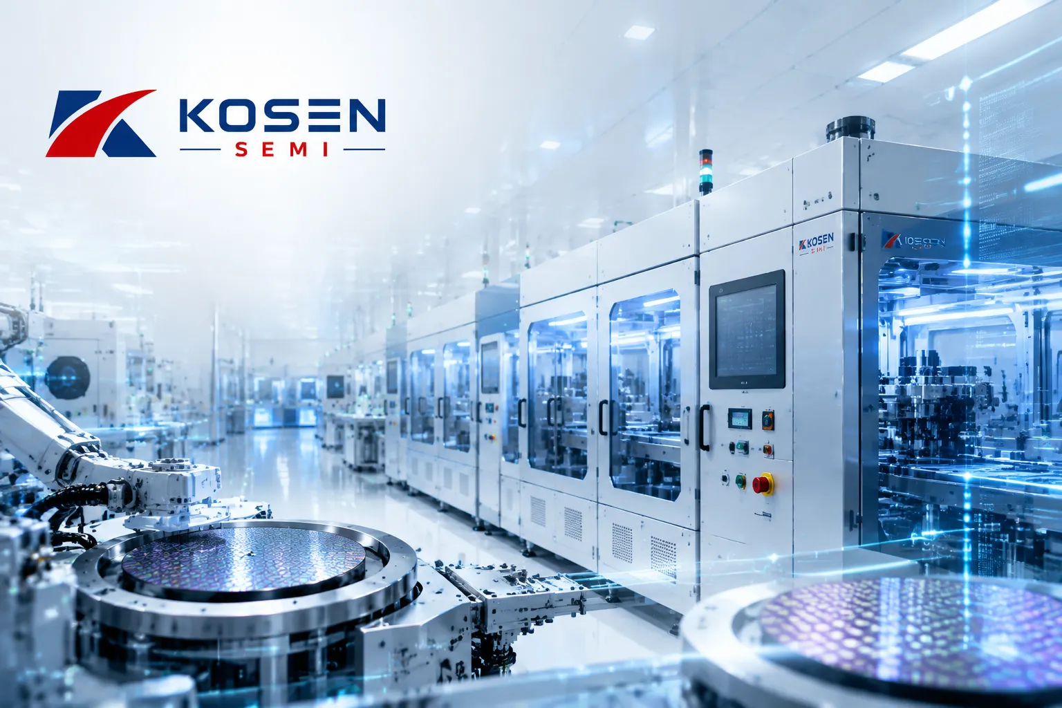
Meeting Stringent Cleanliness and Process Repeatability in Nanometer IC Manufacturing
For established semiconductor fabrication at 200 nm process nodes, with selected applications evaluated down to a 100 nm limit, rigorous microcontamination control directly determines overall fab yield. Metallic impurities and fine particulate residues can disrupt pattern transfer, degrade dielectric integrity, and reduce device yield. KOSEN SEMI engineers advanced chemical dispense and ultra-pure wet etching systems specifically designed to support stable processing across critical cleanroom environments.
Front-End-of-Line Surface Purity Tolerances
In Front-End-of-Line (FEOL) wafer surface cleaning, removing native oxide layers, organic contaminants, and trace metallic ions like iron, copper, nickel, and calcium requires absolute cleanliness down to thresholds below 10⁹ atoms per square centimeter. KOSEN SEMI proprietary fluid control technology combines targeted megasonic acoustic energy with optimized chemical formulations to execute damage-free scrubbing across sensitive, high-aspect-ratio gate topologies.
- • Fine Particle Removal: Prevents lattice dislocations and gate oxide breakdown in leading-edge transistor channels.
- • Chemical Cross-Talk Elimination: Isolated fluid delivery pathways prevent reagent migration between sensitive process steps.
Back-End-of-Line Pre-Metallization Treatment
During Back-End-of-Line (BEOL) interconnect processing, persistent chemical residues and 200 nm-class particulate traps create voids and electromigration risks in copper dual-damascene architectures. Our high-uniformity wet processing platforms deliver precise surface preparation prior to metallization, removing polymeric residues without compromising fragile low-k dielectric constants.
- • Ultra-Pure Wet Etching: Ensures highly isotropic dimensional accuracy across narrow contact vias and trenches.
- • Surface Passivation: Inhibits post-clean surface oxidation prior to barrier layer sputter deposition.
Quantitative Performance Benchmarks
Particle removal performance for 200 nm-class wafer defect density reduction.
Reagent concentration accuracy maintained over continuous bath lifetimes.
Active thermal regulation ensuring highly repeatable reaction kinetics.
Contamination Control Architecture
Review the supported process range and fluid-control parameters for standard 200 nm production and selected applications down to the 100 nm limit.
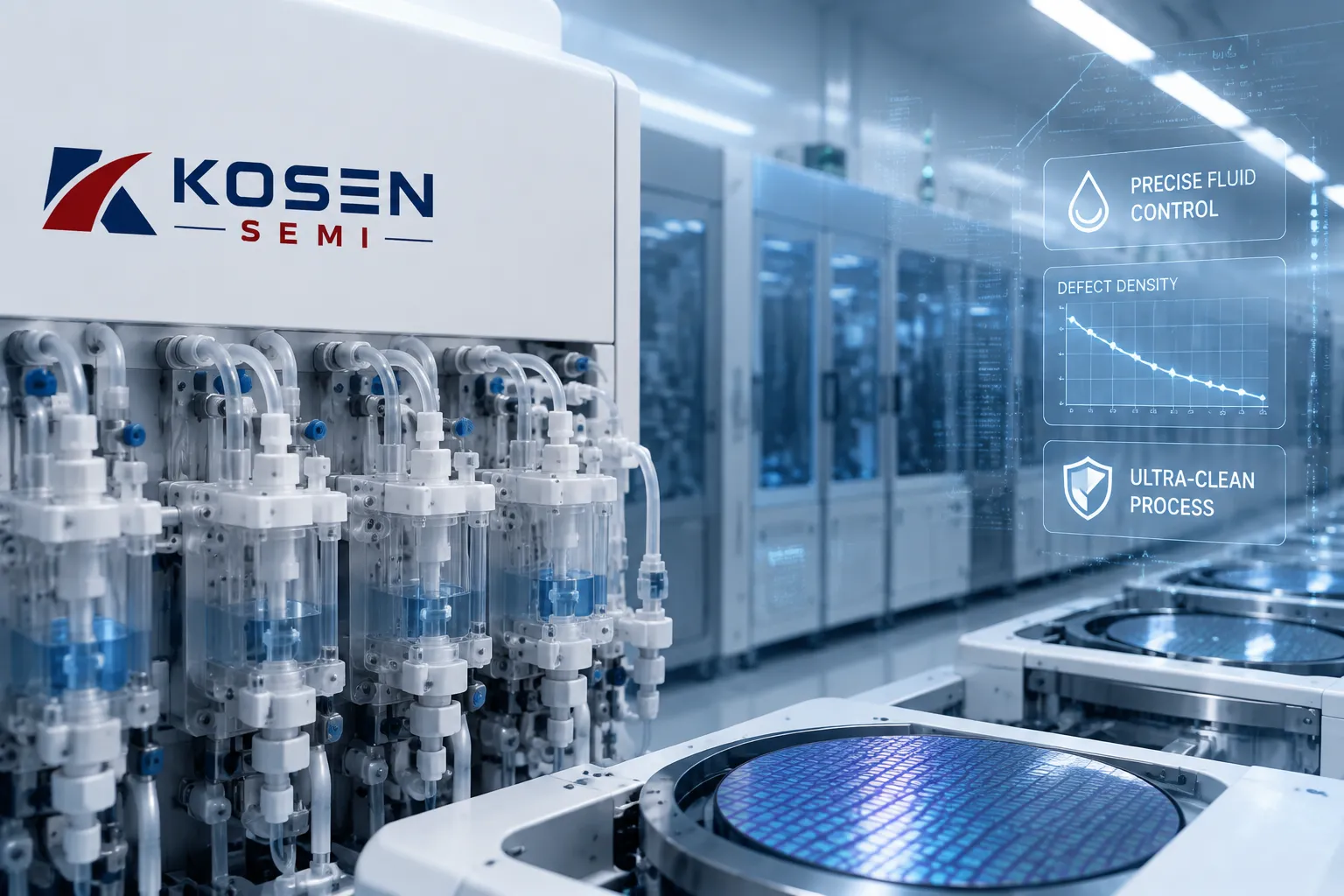
KOSEN SEMI proprietary fluid control technology minimizes defect density across client fabs worldwide.
IC Cleanroom Solutions for 200 nm Production Processes
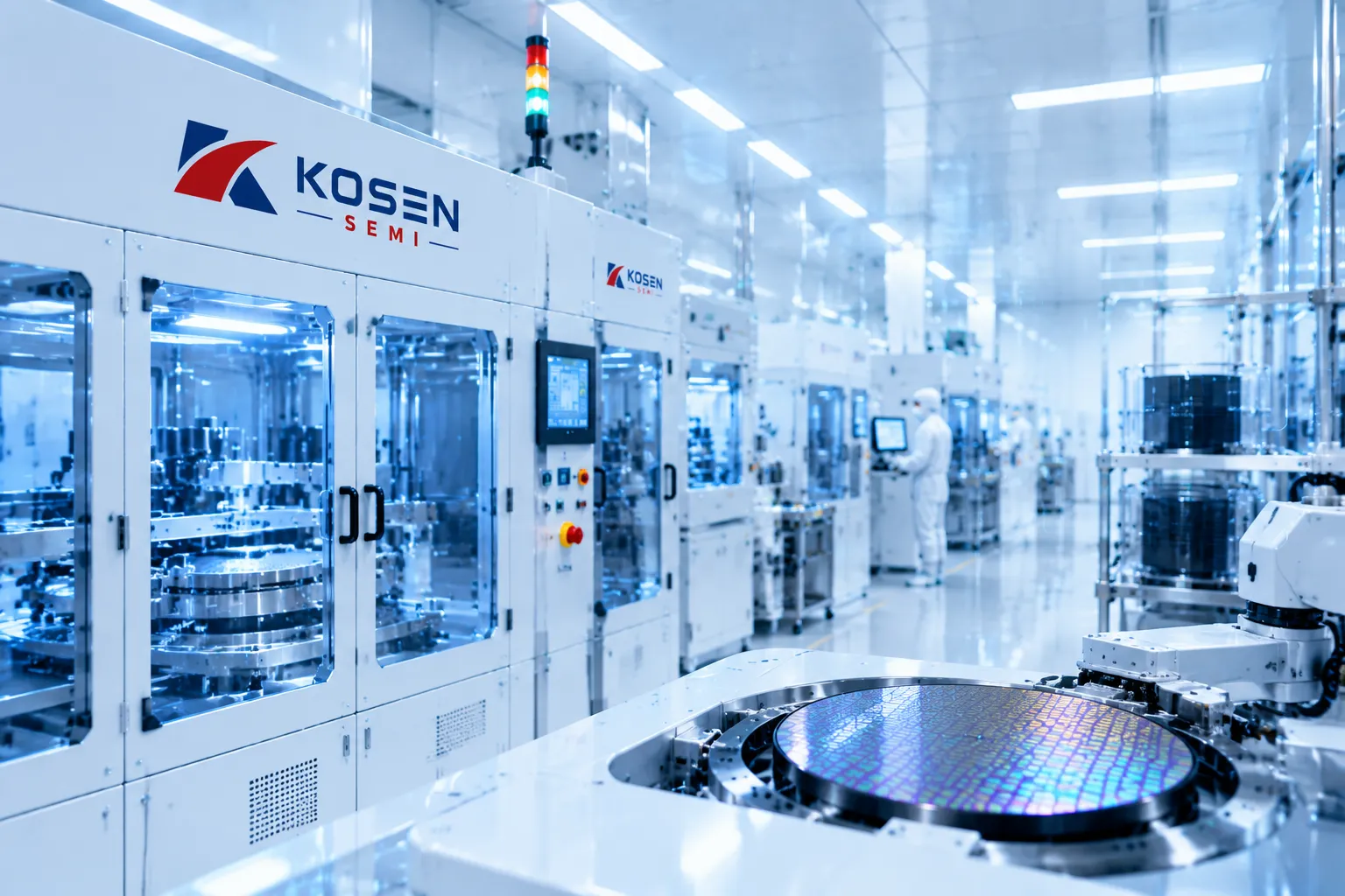
KOSEN SEMI delivers high-purity wet process equipment engineered primarily for 200 nm semiconductor fabrication lines, with selected process evaluations down to a 100 nm limit. Backed by our advanced Engineering Capability, our automated wet benches and Single Wafer Cleaning Systems deliver controlled contamination performance and precise dimensional etching across supported FEOL and BEOL process steps.
FEOL Wafer Surface Cleaning
Eliminate native oxide films, trace metallic ions, and organic contaminants from sensitive silicon substrates prior to oxidation and epitaxy with our advanced wafer-cleaning-systems.
- Consistent fine-particle removal performance
- Ultra-pure chemical delivery & oxide stripping
- Trace metal decontamination to ppt levels
High-Selectivity Wet Etching
Maintain repeatable wet-process control for supported 200 nm device structures and selected applications approaching the 100 nm process limit.
- Extreme chemical selectivities for gate oxide
- Deep trench isolation (DTI) profile control
- Precise temperature stability (±0.1°C)
Damage-Free Photoresist Stripping
Remove high-dose implanted photoresist and post-etch organic residues while protecting supported device structures.
- Heavy polymer residue stripping
- Zero substrate loss & surface passivation
- Extended chemical bath operational life
BEOL Pre-Metallization Treatment
Prepare ultra-pure contact surfaces prior to metal deposition and copper interconnect wiring in high-density IC layouts.
- Pristine contact surface preparation
- Post-CMP slurry residual cleaning
- Low-k dielectric layer integrity protection
Advanced Chemical Dosing Precision
Maintain exact chemical concentration ratios and bath temperatures across continuous, high-volume production cycles.
- Inline concentration monitoring & auto-spiking
- Closed-loop dosing with zero parameter drift
- Reduced chemical consumption & cost
Ultra-Pure Filtration Systems
Eliminate micro-particles and chemical contaminants to safeguard yield stability in advanced semiconductor fab cleanrooms.
- Point-of-use fine-particle filtration
- High-flow recirculating bath chemistry
- Designed for SEMI S2-aligned safety and ISO Class 5–7 cleanroom integration
Wet Processing Systems & Automated Etching Technology Architecture
KOSEN SEMI engineers fully automated wet processing equipment and precision etching platforms engineered specifically for high-yield 200mm (8-inch) and 300mm (12-inch) commercial semiconductor fabrication lines. Designed to meet the stringent contamination control standards of standard 200 nm semiconductor processes and selected applications down to a 100 nm limit, our wet chemistry wafer-cleaning-systems balance microscopic chemical uniformity with ultra-low defect density. Backed by our advanced Engineering Capability, we ensure continuous innovation across all equipment lines. Explore our three flagship equipment lines below to analyze technical specifications, fluid control mechanisms, and yield-enhancement capabilities.
Single-Wafer Spin Processing & Precision Edge Bevel Removal
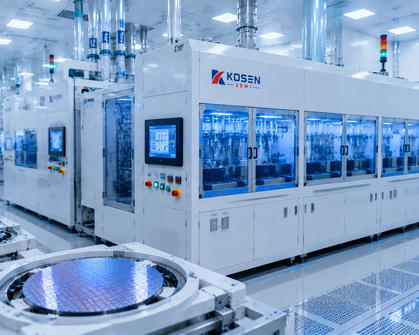
KOSEN SEMI single-wafer wet processing systems deliver unmatched wafer-to-wafer repeatability for critical FEOL and BEOL cleaning and etching steps. By isolating each substrate inside a micro-environment clean chamber, our specialized Single Wafer Cleaning Systems eliminate chemical cross-contamination and enable precise spatial control over fluid temperature, flow velocity, and dispensing profiles.
Key Technical Advantages:- Wafer-to-Wafer Uniformity: Dual chemical dispense arms with dynamic closed-loop flow control maintain stable and repeatable etching uniformity across supported substrates.
- Advanced Edge Bevel Removal (EBR): Integrated high-precision optical tracking nozzles deliver clean edge bevel trimming without wrap-around chemical contamination.
- Micro-Environment Isolation: Sealed processing chambers continuously purged with continuous nitrogen flow help maintain a controlled local processing environment over the active substrate.
- Aggressive Chemical Resistance: Fully compatible with concentrated HF, SPM, SC1, SC2, and specialized solvent chemistry with zero enclosure degradation.
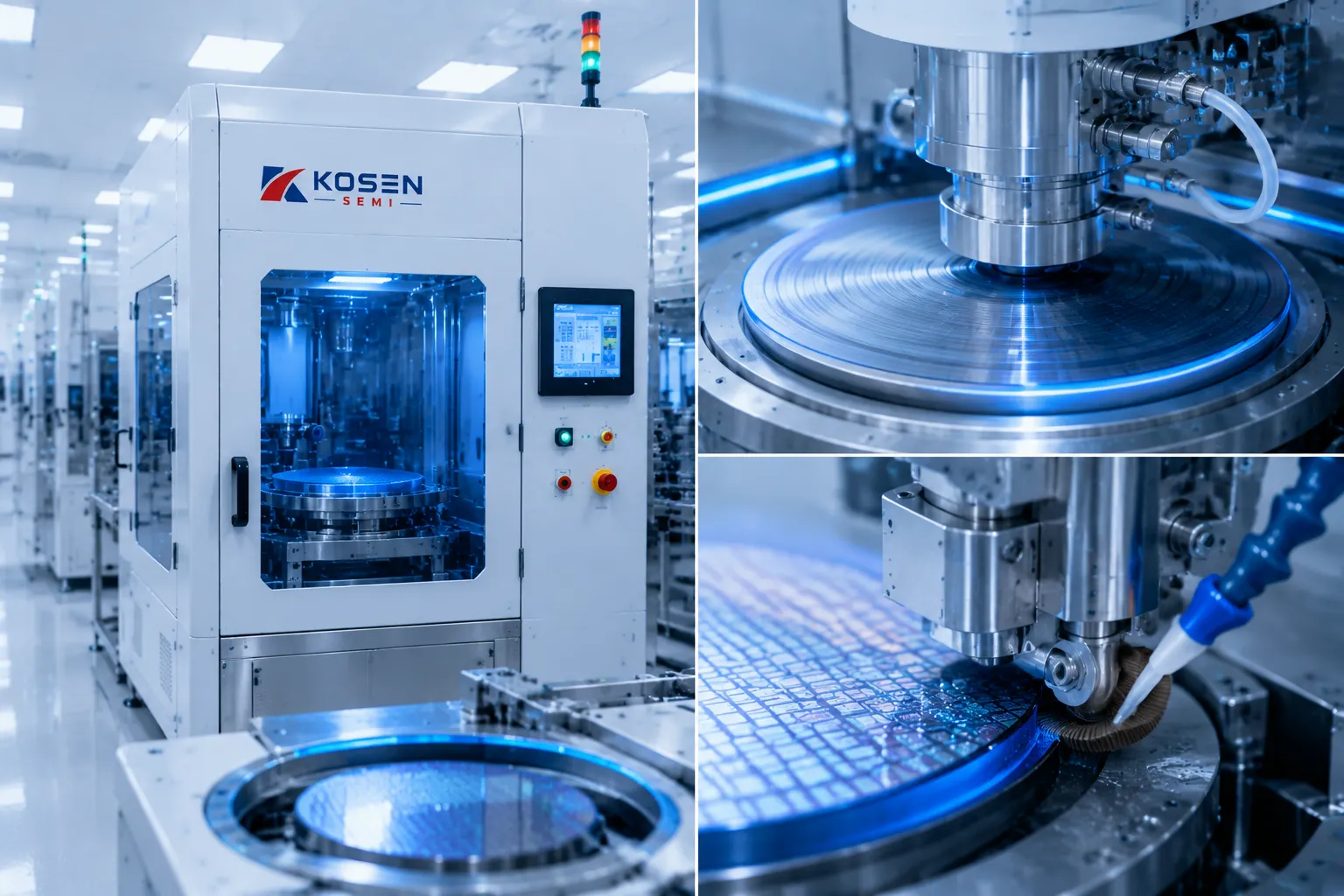
Supports programmable spin rates up to 3,000 RPM with active wafer backside conditioning.
| Specification Parameter | Single-Wafer Platform Performance | Commercial Fab Impact |
|---|---|---|
| Wafer Size Capability | 200mm (8-inch) & 300mm (12-inch) single-substrate chambers | Seamless integration with standard automated material handling systems (AMHS) |
| Etch Uniformity Target | < 1.0% (3-Sigma) across 300mm wafer surface | Supports repeatable processing for 200 nm device structures |
| Particle Removal Efficiency (PRE) | Particle removal performance verified per configured process | Eliminates yield-killing defects prior to critical photolithography steps |
| Edge Bevel Precision | Programmable 0.5mm to 3.0mm width (±0.08mm tolerance) | Protects wafer perimeter during subsequent dielectric film deposition cycles |
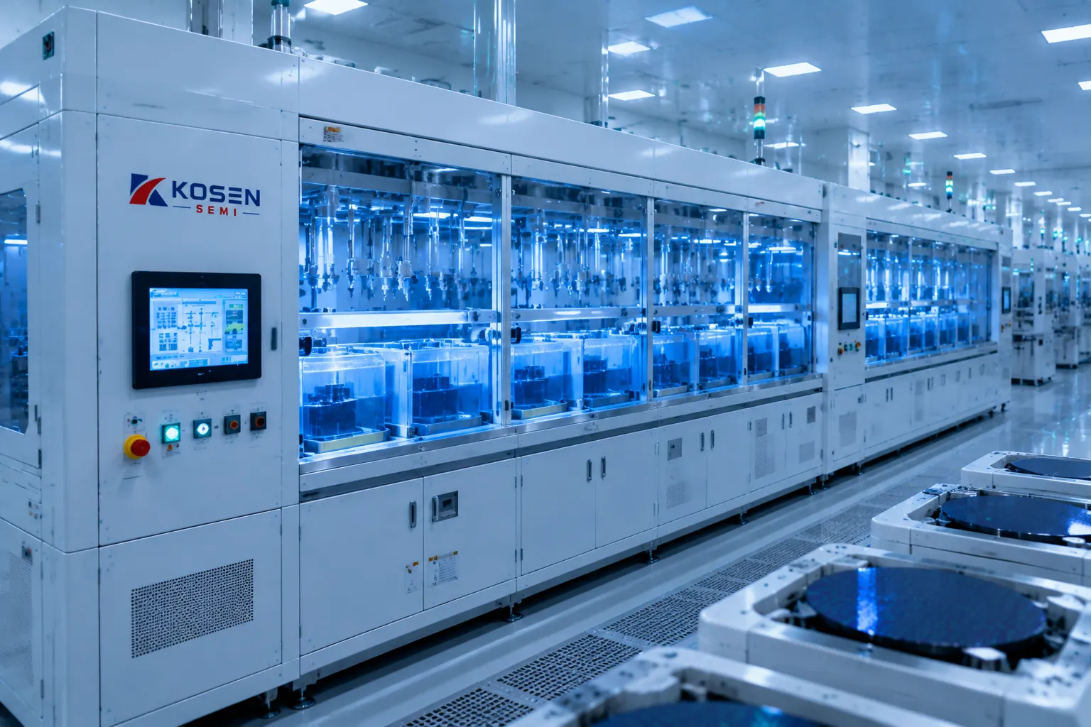
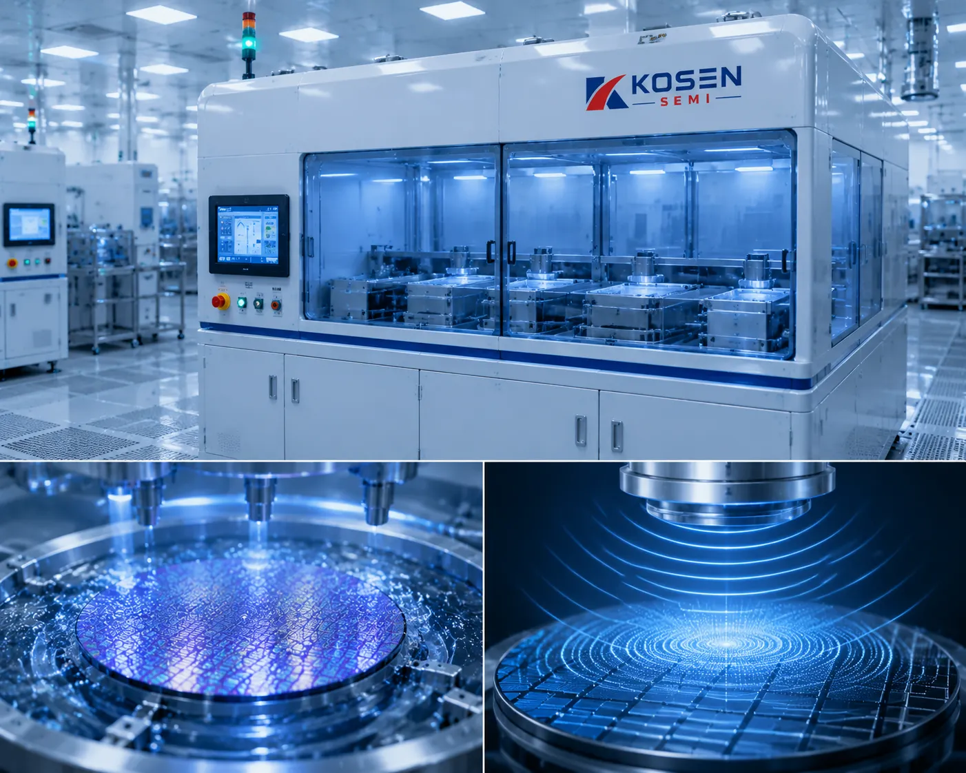
Proven Commercial Fab Integration
KOSEN SEMI automated wet processing platforms are actively deployed in premier 200mm and 300mm semiconductor fabrication lines globally, delivering strict SEMI S2/S8 compliance and measurable yield enhancements.
Cleanroom Integration & Process Stability Benchmarks
Support fab procurement and process engineering reviews with documented cleanroom integration requirements, equipment safety features, and process-stability data.
Operational Uptime
Certified Compatibility
Global Fab Field Support
Semiconductor Equipment Certifications
KOSEN SEMI guarantees full compliance with global semiconductor manufacturing safety, ergonomic, and quality engineering standards.
SEMI S2 Standard
Full environmental, health, and safety (EHS) compliance for semiconductor equipment and hazardous chemical distribution.
SEMI S8 Standard
Ergonomic engineering that optimizes operator safety, human-machine interaction, and routine maintenance accessibility.
ISO 9001 Quality Management
Rigorous quality control systems providing precision component repeatability, supply chain traceability, and process reliability.
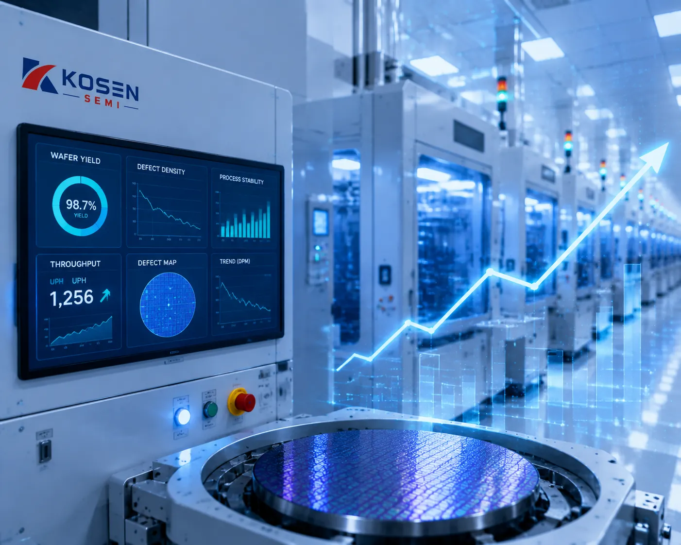
Proven Wafer Yield Optimization & Defect Reduction
Documented performance metrics from high-volume 300mm wafer fabrication lines show immediate defect reduction following KOSEN SEMI wet processing system integration, including advanced Single Wafer Cleaning Systems deployment.
IC Cleanroom Equipment FAQ & Technical Selection Guide
Expert engineering guidance on microcontamination control, fluid delivery safety, damage-free megasonic cleaning, and Site Acceptance Testing (SAT) validation timelines for established semiconductor wafer fabs. Learn more about our core focus and mission.
| Equipment Architecture | Target Application | Cleanroom Rating | Chemistry Support | Yield Advantage |
|---|---|---|---|---|
| Single Wafer Cleaning Systems | FEOL surface cleaning, high-uniformity wet etching, EBR | ISO Class 5–7 Compatible | Dilute HF, SC1, SC2, Specialty Solvents | Reduced cross-contamination risk through individualized wafer processing |
| Automated Batch Wet Bench | High-throughput photoresist stripping, oxide etching, chemical baths | ISO Class 5–7 | SPM, Concentrated HF, Hot Phosphoric Acid | Maximized WPH throughput & automated chemical bath recycling |
| Megasonic Physical Cleaning System | 200 nm-class defect removal, optimized to 100 nm on high-aspect-ratio (HAR) topologies | ISO Class 5–7 Compatible | DI Water, Ozonated Water (DI-O3), Dilute SC1 | Damage-controlled cleaning for supported 200 nm process applications |
01 How do KOSEN SEMI wet processing systems control secondary particle contamination in ISO Class 5–7 environments?
Secondary microcontamination inside ultra-clean semiconductor fabrication lines is eliminated through a multi-tiered engineering protocol built into every KOSEN SEMI tool architecture:
- Aerodynamic Laminar Isolation: Where specified, localized mini-environment enclosures use HEPA or ULPA filtration and controlled vertical airflow to reduce turbulence and airborne particle deposition around critical process zones.
- High-Purity Fluoropolymer Fluid Paths: All chemical contact surfaces utilize semiconductor-grade PFA, PTFE, and high-purity quartz, completely preventing metallic ion leaching and plasticizer outgassing.
- Mag-Lev Fluid Transfer Systems: Seal-less, magnetic levitation pumps eliminate mechanical friction and particle generation in ultra-pure chemical supply lines.
- Point-of-Use (POU) Filtration: Closed-loop chemical recirculation features POU PTFE membrane filters selected according to the required process and cleanliness specification.
02 What process controls protect delicate high-aspect-ratio (HAR) structures during megasonic cleaning and wet etching?
For supported 200 nm processes and selected applications approaching the 100 nm limit, fragile gate structures and HAR trenches risk pattern collapse from surface tension and uncontrolled acoustic cavitation. KOSEN SEMI protects critical topologies through precise fluid dynamic and energy controls across our advanced wafer cleaning systems:
- Frequency-Swept Megasonic Energy: Digital generators sweep acoustic frequencies between 0.8 MHz and 3.0 MHz to distribute energy uniformly without destructive cavitation energy spikes.
- Boundary-Layer Fluid Dynamics: Dynamic chemical dispense nozzles precisely regulate fluid velocity across spinning wafers, mitigating shear stress on supported wafer features.
- Marangoni & IPA Vapor Drying: Surface tension reduction technology utilizes isopropyl alcohol (IPA) vapor gradients to draw liquid out of deep trenches cleanly, bypassing capillary forces that cause line bending.
03 Which aggressive chemistries (e.g., HF, SPM, SC1, SC2) are supported by your automated chemical delivery and anti-corrosion cabinet designs?
KOSEN SEMI automated chemical delivery cabinets and processing modules are engineered to safely supply and recirculate the semiconductor industry's most aggressive wet etching and cleaning formulations:
Hydrofluoric Acid (HF), Sulfuric Acid Peroxide Mixture (SPM), Standard Clean 1 (SC1: NH4OH/H2O2/H2O), Standard Clean 2 (SC2: HCl/H2O2/H2O), and Buffered Oxide Etch (BOE).
N-Methyl-2-pyrrolidone (NMP), photoresist strippers, and specialty solvent formulations requiring active nitrogen purging and static hazard mitigation.
System cabinets are constructed from ECTFE, PVDF, and FM 4910-certified flame-retardant polypropylene. They feature dual-containment fluid lines, real-time chemical concentration monitoring (±0.05% accuracy), active exhaust scrubbing, and automated dosing to extend bath life safely.
04 What is the typical lead time, installation process, and site acceptance testing (SAT) validation timeline for new fab installations?
Standard equipment lead times range from 16 to 24 weeks depending on tool customization and cleanroom automation integration. Our structured fab deployment protocol follows four synchronized phases:
- Engineering Alignment & FAT (Weeks 1–16): Custom CAD layout verification, chemical line routing planning, tool manufacturing, and Factory Acceptance Testing (FAT) at KOSEN SEMI facilities.
- Delivery & Cleanroom Move-In (Weeks 17–18): Crated cleanroom transport, positioning inside client fab bay, and leveling on isolated vibration pads.
- Hook-Up & Safety Verification (Weeks 19–20): Facility utility hook-up, exhaust balancing, double-containment pressure testing, and SEMI S2/S8 compliance checks.
- Site Acceptance Testing (SAT) & Yield Tuning (Weeks 21–23): Particle count qualification on test wafers, process recipe matching, chemical dispense calibration, and official client sign-off.
Need Customized Fab Integration Advice?
Speak directly with a KOSEN SEMI Process Engineer to evaluate your wafer throughput requirements, chemistry specs, or cleanroom retrofit constraints.
Schedule an IC Fab Equipment Consultation
Submit your wafer process parameters, cleanroom specifications, and target throughput requirements. A KOSEN SEMI semiconductor process engineer will deliver a detailed technical evaluation within 24 hours.
24-Hour Engineering Turnaround
Rapid process matching and custom equipment configuration proposals, supported by our advanced Engineering Capability.
High-Yield Cleanroom Solutions
SEMI S2/S8 compliant systems tailored for advanced IC fab integration.