
Advanced Semiconductor Packaging Cleaning & Precision Contamination Control
Control 200 nm-class particles, with optimized removal down to 100 nm, organic residues, and flux contaminants across sub-10µm fine-pitch 2.5D, 3D, and Chiplet architectures. KOSEN SEMI delivers application-engineered wet process equipment and automated chemical delivery systems to optimize yield for leading global packaging fabs.
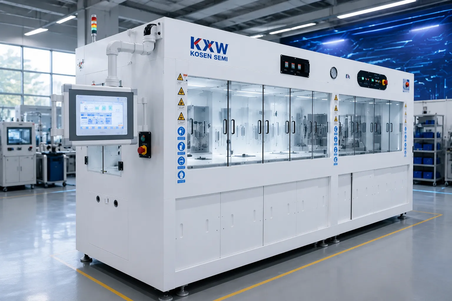
Modern high-density semiconductor architectures demand uncompromising cleanliness to prevent yield loss caused by 200 nm-class contaminants, with optimized removal down to 100 nm, organic residues, and flux debris. KOSEN SEMI advanced packaging cleaning solutions fully adapt to various heterogeneous integration and high-density packaging architectures, helping global packaging fabs overcome critical technical bottlenecks and achieve high-reliability interconnections.
2.5D / 3D & TSV Packaging
Targeting silicon interposers and Through-Silicon Vias (TSV) with high aspect ratios (> 10:1) where deep micro-hole residues impair interconnect integrity. Specialized low-surface-tension chemistry and directed megasonic energy overcome surface barriers to resolve deep hole blind-spot penetration and drying challenges without structural degradation. Learn more about our advanced wafer cleaning systems designed for complex architectures.
- TSV Residue Penetration: Effective fluid exchange in aspect ratios exceeding 10:1.
- Watermark-Free Drying: Advanced Marangoni IPA drying leaves zero surface stains.
- Yield Preservation: Eliminates trapped CMP slurry and organic contaminants in deep blind vias.
Chiplet Heterogeneous Integration
Tailored for ultra-fine Microbump pitches under 20 μm where flux residues and organic contaminants lead to bonding opens and electrical shorts. KOSEN SEMI advanced wet bench systems for microbump flux removal balances precise chemical concentration with gentle acoustic agitation to safeguard delicate micro-joints.
- Sub-20 μm Penetration: Dissolves synthetic and rosin flux in narrow microbump gaps.
- Zero Physical Shear: Non-destructive physical cavitation prevents bump deformation or shear.
- Die Bonding Integrity: Ensures pristine pad contact areas for high-density multi-die integration.
Fan-Out Wafer & Panel Packaging (FOWLP/FOPLP)
Engineered for Redistribution Layer (RDL) processing across 300mm round wafers and large rectangular glass/organic panel substrates. KOSEN SEMI chemical cleaning equipment and fan-out wet processes systematically remove photoresist scum, organic residue, and metallic micro-particles to guarantee reliable multi-die interconnectivity.
- 200 nm-Class Particle Stripping: Complete photoresist residue and metallic debris removal.
- Panel & Wafer Compatibility: Fully adaptable to 300mm wafers and 510x515mm FOPLP panels.
- Dielectric Surface Activation: Prepares copper redistribution lines for pinhole-free plating.
Flip Chip BGA & High-Density Soldering
Focusing on the narrow standoff space underneath solder bumps prior to capillary underfill (CUF). Trapped organic residues or micro-particulates cause voiding and void-induced delamination. KOSEN SEMI semiconductor wet bench systems clean underfill gaps down to 15 μm, delivering pristine surface energy for optimal epoxy flow and adhesion.
- Underfill Void Elimination: Surface preparation reduces capillary flow voids down to zero.
- Contact Angle Optimization: Achieves water contact angles below 10 degrees for complete wetting.
- High Volume Throughput: Batch wet bench and inline configurations deliver low Cost of Ownership (CoO).
Architectural Process Specifications Comparison
Different advanced packaging routes require targeted chemical energy, specialized megasonic acoustic fields, and watermark-free drying protocols. Below is a structured cross-reference detailing how KOSEN SEMI addresses critical process challenges across high-density semiconductor packaging architectures. Our company focuses on driving manufacturing yield improvements across all global markets.
- Chemical penetration in sub-10μm narrow gaps
- 200 nm-class particulate & scum suppression
- Zero bump shear stress or chemical corrosion
- 100% watermark-free Marangoni surface drying
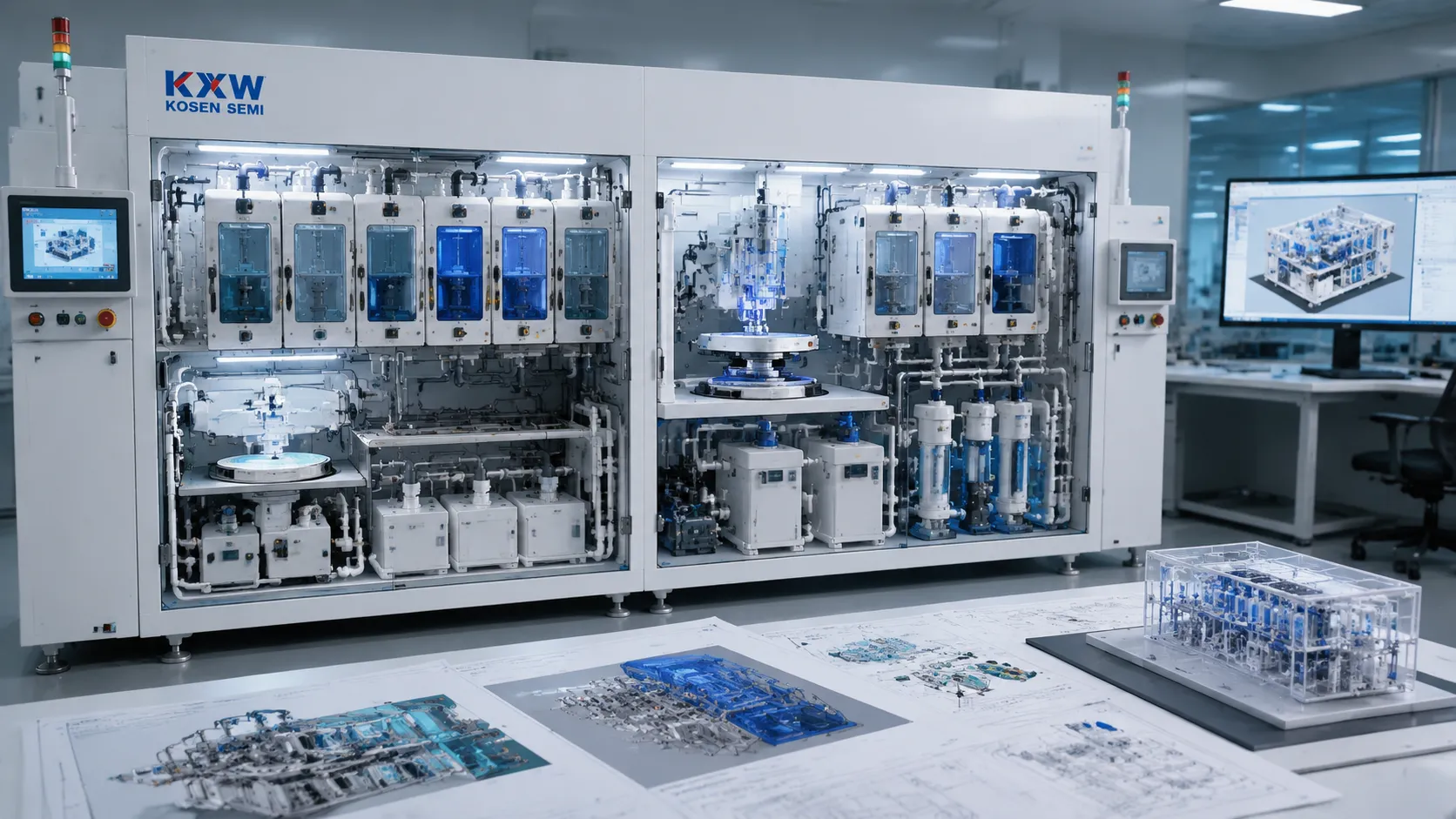
| Packaging Route | Primary Contaminants | KOSEN SEMI Wet Process Mechanism | Yield Impact |
|---|---|---|---|
| 2.5D / 3D & TSV | Deep via slurry residue & micro-flux debris | Megasonic cavitation & low surface tension solvents | Via connectivity failure down to 0% |
| Chiplet Integration | Microbump rosin & organic film residue | Active fluid dynamic recirculation & gentle cavitation | Prevents joint open/short faults |
| FOWLP / FOPLP | Photoresist scum & metallic micro-particles | Single-wafer chemical strip & ultrapure water rinse | +15% line yield enhancement |
| Flip Chip BGA | Narrow gap flux & airborne particulates | Surfactant-assisted flushing & Marangoni IPA drying | Zero underfill voiding |
Tailored Cleaning Systems for Every Advanced Packaging Line
Whether your facility focuses on high-volume consumer Flip Chip production, High Bandwidth Memory (HBM) 3D TSV stacking, or heterogeneous Chiplet modules, contamination control remains the single largest determinant of final line yield. As an industry-leading semiconductor wet-process equipment OEM, KOSEN SEMI delivers customized Single Wafer Cleaning Systems, multi-tank wet benches, and automated chemical dosing units designed to integrate seamlessly into modern packaging fabs. Contact our process application lab to evaluate your specific flux chemistry and substrate parameters.
Core Cleaning Process Technologies and 200 nm Contamination Control Capabilities, Optimized to 100 nm
As advanced semiconductor packaging transitions toward 2.5D, 3D, and Chiplet heterogeneous architectures, physical tolerances for surface contamination reach 200 nm production dimensions, with optimized capability down to 100 nm. Fine-pitch microbumps, redistribution layers (RDL), and high-aspect-ratio Through-Silicon Vias require cleanroom-certified wet process methodologies that thoroughly eliminate organic residues without inflicting structural damage on delicate metallic interconnects.
At KOSEN SEMI, our engineered wafer cleaning systems merge dynamic megasonic field control, low-surface-tension chemistry compatibility, watermark-free Marangoni drying, and real-time fluid metrology to maintain maximum line yield across demanding advanced packaging workflows.
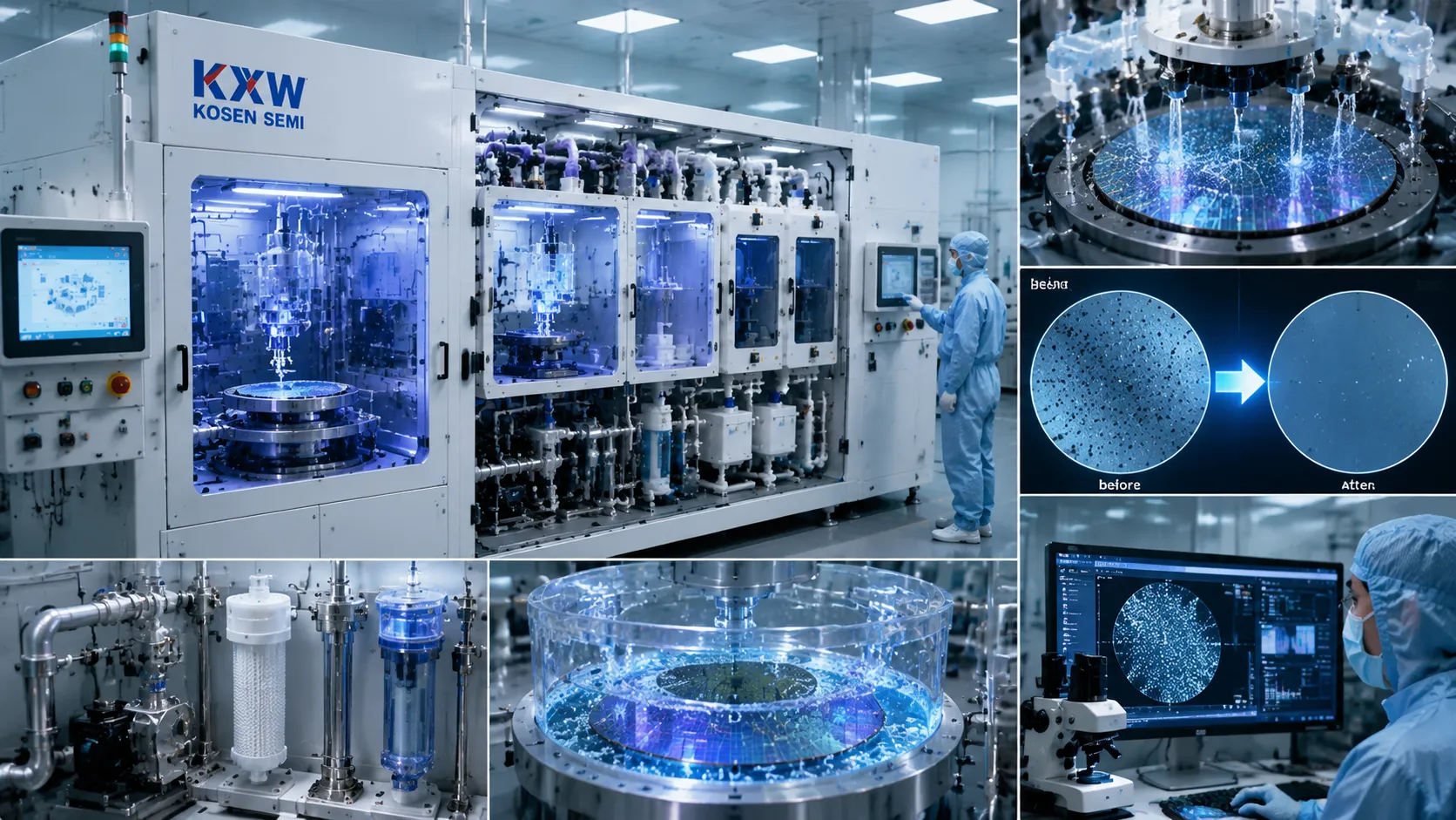
Contamination Control Highlights
Megasonic Cavitation Tuning for Microbump Residue Removal
Conventional low-frequency ultrasonic cleaning generates violent collapse bubbles that easily shatter fragile copper pillars, solder microbumps, and ultra-thin Redistribution Layer lines. To prevent physical stress damage while achieving complete microbump residue removal, our high-precision megasonic systems operate across the 0.8 MHz to 3.0 MHz acoustic spectrum.
By dynamically modulating acoustic wave distribution and controlling boundary layer fluid velocity, micro-streaming energy flows evenly into narrow spaces beneath multi-chip assemblies without creating destructive transient cavitation. Discover more about our advanced Single Wafer Cleaning Systems designed for ultimate target precision.
Key Technical Capabilities
- • Multi-frequency sweep technology: Eliminates acoustic standing-wave blind spots to ensure uniform cleaning across the entire wafer surface.
- • Closed-loop energy density control: Real-time transducer feedback maintains energy uniformity within tight thresholds to safeguard high-aspect-ratio structures.
- • Selective pulse profiling: Tailors acoustic power to match sensitive substrate metallization including copper, aluminum, and nickel-gold layers.
Ultra-Low Surface Tension Penetration and Flux Residue Removal
In Chiplet and 2.5D packaging, solder reflow leaves behind complex flux residue cleaning challenges in micro-gaps narrower than 10 micrometers. Standard aqueous rinses cannot overcome high surface tension barriers to enter these narrow underfill spaces effectively.
Our wet process benches utilize engineered chemical formulations designed with ultra-low surface tension. These specialized chemistries quickly wet hydrophobic flip-chip surfaces, chemically break down cross-linked organic polymers, and suspend particulate matter for swift fluid extraction.
Key Technical Capabilities
- • Micro-gap wetting agents: Flushes narrow underfill gaps to prepare clean contact surfaces for secondary capillary underfill encapsulation.
- • Corrosion-inhibited chemistry: Prevents oxidation or etching on sensitive exposed copper pillars, solder bumps, and pad interfaces.
- • Polymer residue dissolution: Efficiently strips hardened photoresist remnants and organic contaminants without damaging delicate dielectric layers.
Watermark-Free Marangoni Drying for 200 nm Particle Removal, Optimized to 100 nm
Drying fine-pitch substrates is one of the most critical stages in 200 nm-class particle cleaning, with optimized capability down to 100 nm. Liquid droplets trapped between closely spaced microbumps cause watermark defects, ion migration, and localized oxidation if evaporated improperly.
KOSEN SEMI integrates advanced IPA Marangoni drying technology that introduces a precise surface tension gradient at the liquid-vapor-wafer interface. As the wafer slowly emerges from the ultra-pure water rinse bath, the surface tension gradient draws liquid away smoothly, leaving a completely dry, zero-residue surface.
Key Technical Capabilities
- • Zero-watermark drying: Leaves no drying marks or mineral deposits on high-density microbump arrays down to fine pitches.
- • Controlled secondary redeposition risk: Prevents dissolved particles or airborne contaminants from re-attaching during fluid extraction.
- • High surface free energy activation: Prepares pristine dielectric and metallic surfaces to optimize subsequent underfill flow and wire bonding adhesion.
Real-Time Chemical Dosing and Inline Metrology Integration
Maintaining tight process windows requires continuous monitoring of chemical bath concentration, fluid temperature, and inline particle counts. Degradation in chemical potency directly impacts cleaning consistency across high-volume manufacturing runs.
Our inline Chemical Dosing System constantly samples bath chemistry using spectroscopic sensors and refractive index monitors. Automated replenishment algorithms compensate for chemical consumption and evaporation, guaranteeing identical process performance from the first wafer to the last. Built upon our core Engineering Capability, this continuous control ensures strict quality standards.
Key Technical Capabilities
- • Automated concentration control: Maintains active chemical concentration within strict accuracy tolerances for reproducible process windows.
- • In-situ particle detection: Monitors bath cleanliness in real time with automated alarm triggers and dynamic filtration recycling.
- • SECS/GEM MES integration: Enables comprehensive tracking of process parameters for complete traceability in advanced semiconductor packaging.
Dedicated Packaging Wet-Process Equipment & Automated System Selection
Engineered for 2.5D/3D SiP, Chiplet, and FOWLP packaging lines. KOSEN SEMI delivers high-yield contamination control through our complete line of semiconductor packaging products, featuring modular single wafer cleaners, high-throughput wet benches, and automated chemical dosing systems.
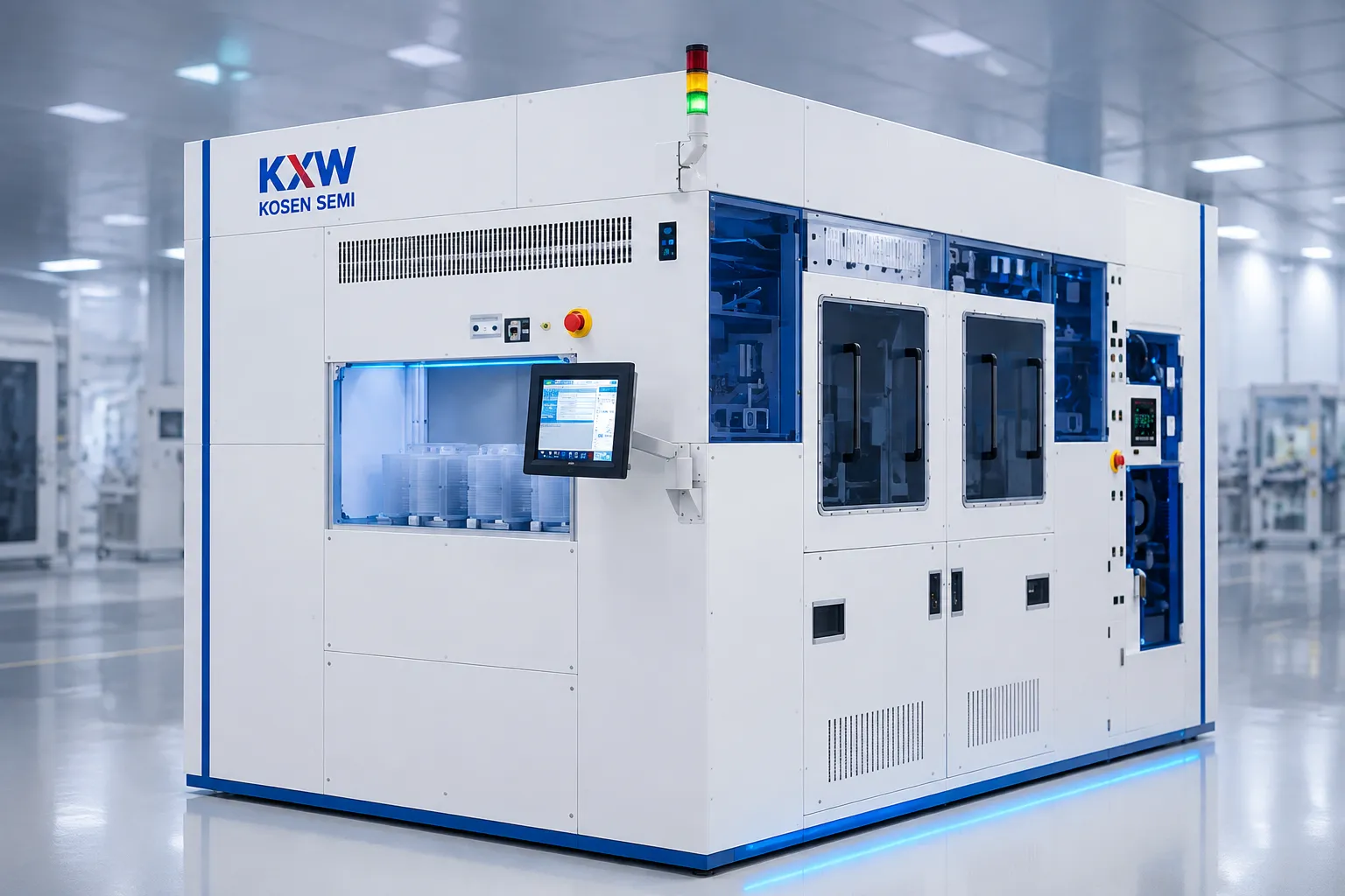
Single Wafer Cleaner for Microbump & 3D Chiplet
Delivers isolated single-wafer processing with controlled megasonic and high-pressure spray for zero-cross-contamination cleaning of microbumps under 10µm. Explore our advanced wafer cleaning systems to optimize your yields.
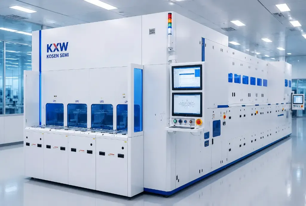
Automated High-Throughput Advanced Packaging Wet Bench
Multi-tank batch immersion system engineered for high-volume FOWLP and Flip Chip lines, offering high wafer throughput and ultra-low Cost of Ownership (CoO).
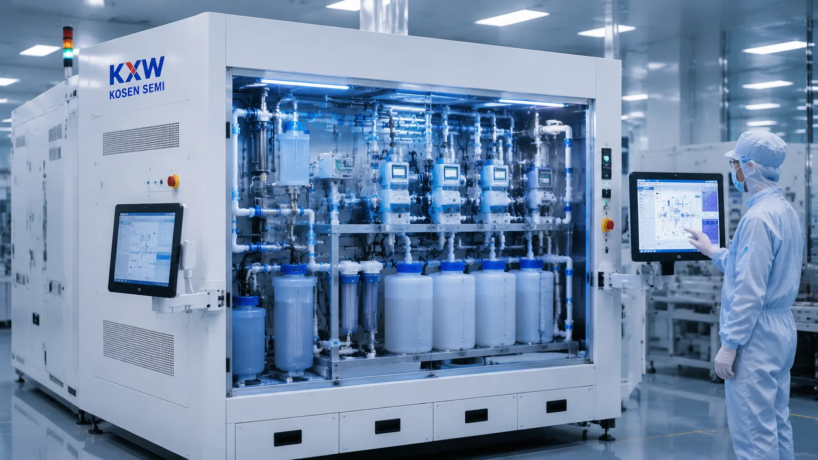
Automated Chemical Dosing & Recirculation System
Precision real-time blending, continuous closed-loop filtration, and chemical recirculation designed to minimize chemical consumption and ensure process stability.
SECS/GEM Compliant for Smart Semiconductor MES Integration
Every KOSEN SEMI advanced packaging wet bench, single wafer cleaner, and automated chemical dosing system features native SECS/GEM interface capabilities, supported by our core Engineering Capability to ensure fully automated, traceable, and modular deployment for next-generation semiconductor packaging fabs.
Quality Assurance, Test Data and ISO 14644 Cleanroom Standards
At KOSEN SEMI, high-reliability packaging and rigorous contamination control define our engineering philosophy. We have established a comprehensive semiconductor application test laboratory, utilizing strict SEMI standards to provide reliable process verification and data support. Every wet processing system engineered for advanced semiconductor packaging cleaning undergoes exhaustive laboratory validation to achieve semiconductor yield optimization while safeguarding delicate microbumps, Redistribution Layers (RDL), and high-aspect-ratio features against damage.
Application Laboratory Testing Services
Eliminating process uncertainty requires empirical proof before production scaling. KOSEN SEMI provides complimentary pre-production Sample Testing and Residue Analysis reports for advanced 2.5D, 3D SiP, Chiplet, and FOWLP architectures. Our application lab evaluates your specific substrate materials, fine-pitch microbumps (<10 µm), and specialized flux formulations to engineer optimized chemical dosing and megasonic wet process recipes. Learn more about us and our commitment to advanced process control.
- ✓ Pre-Production Sample Cleaning: Comprehensive bench testing on customer-supplied wafers, panels, and interposers under simulated cleanroom production conditions.
- ✓ Quantitative Residue Analysis: High-precision chemical and particle analytical reports evaluating particle removal performance down to 100 nm under optimized conditions.
- ✓ Zero Substrate Damage Guarantee: Multi-frequency megasonic energy field mapping to prevent physical pitting or erosion on sensitive Cu, Al, and Ni/Au metallization.
Cleanroom Cleanliness and Compliance Standards
Contamination control begins long before equipment reaches customer facilities. KOSEN SEMI executes equipment manufacturing, precision assembly, and final testing within controlled ISO Class 5–7 cleanroom environments. Our procedures adhere strictly to ISO 14644 cleanroom standards and international semiconductor safety directives, eliminating cross-contamination risk for ultra-clean manufacturing environments.
Controlled assembly and validation
Ergonomics and hazard control
Semiconductor yield optimization
Certified Standards and Verification Framework
| Standard / Certificate | Verification Scope | Customer Impact |
|---|---|---|
| ISO 14644-1 | Airborne particulate cleanliness control | Supports controlled cleanroom performance during installation |
| SEMI S2 & S8 | Environmental, health, safety, and ergonomics | Ensures smooth Fab utility integration and operator safety |
| CE Compliance | European electrical and mechanical safety rules | Standardized global operational readiness and safety |
| ISO 9001:2015 | Quality management system across production | Consistent tool-to-tool reproducibility and reliability |
Microscopic SEM Visual Inspection Comparison
Drag the interactive slider below to inspect Scanning Electron Microscope (SEM) imaging around fine-pitch microbumps before and after KOSEN SEMI precision wet cleaning.
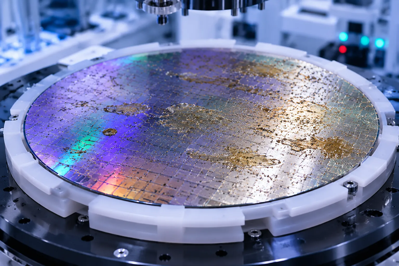
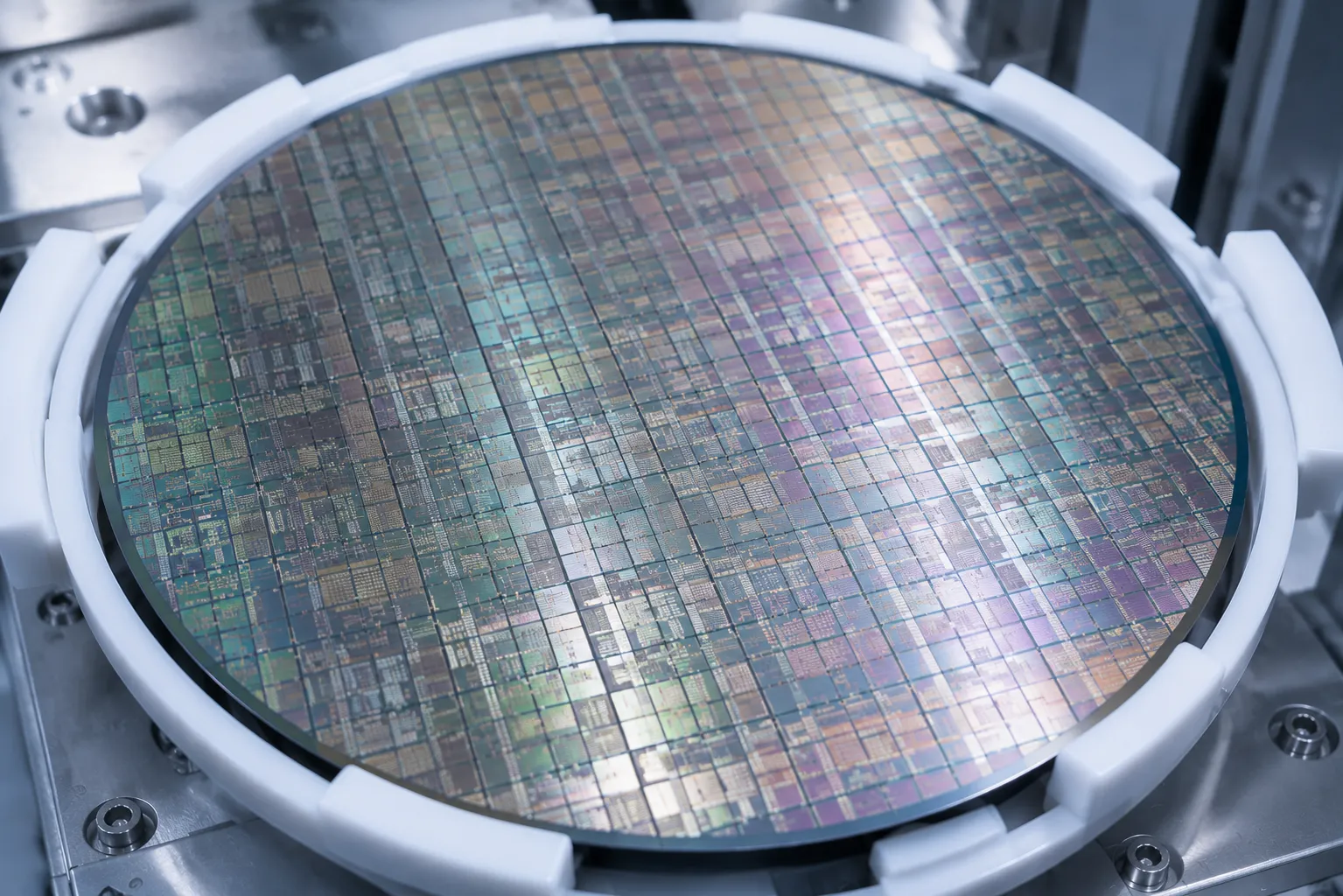
Targeting fine microbump pitch (<10 µm) and narrow underfill gaps. Pre-clean surface reveals heavily polymerized flux residues and 200 nm-class particulates causing electrical bridge risks. Post-clean evaluation demonstrates verified surface cleanliness for high-reliability packaging without substrate pitting or bump undercut.
Certifications and Quality Credentials
Schedule Your Application Test
Send your sample substrates to our application laboratory for a complete cleaning feasibility study, surface analysis, and process optimization proposal tailored to your packaging line.
Request Sample Testing Service→Advanced Packaging Cleaning FAQ
Our technical expert team at KOSEN SEMI has compiled detailed operational answers based on years of packaging line deployment experience to ensure your process transition is seamless, safe, and optimized for maximum yield. Learn more about-us and our commitment to advanced semiconductor processing.
Preventing surface oxidation, galvanic corrosion, and pad undercutting on sensitive microbumps composed of Copper, Aluminum, or Tin-Silver alloys requires a multi-layered chemical and physical process control approach. KOSEN SEMI advanced packaging cleaning systems integrate automated pH-buffered chemistry dosing, proprietary oxidation inhibitors, and continuous inert nitrogen gas shrouding throughout rinse sequences.
Our closed-loop chemical recirculation architecture monitors oxidation-reduction potential in real time to prevent metallic degradation while removing cured organic residues. Coupled with non-destructive Megasonic field management, our microbump flux removal equipment ensures complete contaminant dissolution under fine-pitch constraints without inducing mechanical micro-fractures or physical pitting. Discover our full range of high-performance wafer-cleaning-systems designed for high-density architectures.
Maintains tight pH ranges to halt acid or alkaline etching on active substrate metallization.
Eliminates dissolved oxygen during heated DI water rinse stages to stop re-oxidation.
Controlled acoustic pressure fields prevent physical pitting on delicate bump metallurgy.
In 2.5D and 3D heterogeneous integration architectures, Through-Silicon Vias feature high aspect ratios and deep blind-hole geometries that create significant fluid surface tension barriers. Traditional spray systems often fail to overcome air entrapment, resulting in incomplete residue removal and sub-surface reliability defects.
To address this challenge, our TSV residue cleaning system utilizes ultra-low surface tension wet chemical formulations combined with synchronized Megasonic acoustic streaming and vacuum-assisted fluid evacuation. The acoustic pressure waves drive chemical penetration deep into micro-vias, dissolving photoresist residues and metallic particles. Subsequent high-efficiency IPA Marangoni drying leverages surface tension gradients to evacuate trapped liquids completely, leaving zero watermarks or secondary particle redeposition.
- Particle removal down to 100 nm under optimized, application-qualified conditions
- Integrated Marangoni surface tension gradient drying for watermark-free output
- Optimized for aspect ratios exceeding 10:1 in advanced interposer designs
Yes. KOSEN SEMI provides comprehensive process recipe evaluation services through our state-of-the-art semiconductor application test laboratories. Because flux compositions, polymers, and photoresist chemistries vary significantly between advanced packaging lines, custom recipe development is essential to achieve optimum cleanroom yield optimization.
Our process engineers perform complimentary pre-production sample testing using customer-supplied wafers or substrates. We utilize advanced Scanning Electron Microscopy and Atomic Force Microscopy surface inspections to verify complete particle removal, surface energy levels, and electrical contact integrity before equipment configuration.
Application Lab Evaluation Protocol
All KOSEN SEMI semiconductor wet process bench systems and Single Wafer Cleaning Systems are engineered with compact modular footprints to maximize cleanroom floor efficiency. Built specifically for high-density fab layouts, our equipment minimizes utility hookup requirements while providing high throughput capability.
Our tools strictly adhere to international semiconductor manufacturing safety and environmental standards. Systems are manufactured in ISO Class 5–7 cleanroom environments and carry full compliance certification for SEMI S2 environmental health and safety guidelines, SEMI S8 ergonomics, and FM4910 fire-retardant plastic material construction standards.
Consult with KOSEN SEMI packaging wet process specialists to analyze your yield parameters and request sample testing.