
Semiconductor Case Studies: Proven Wet Process Results
Discover how KOSEN SEMI empowers global semiconductor fabs with high-precision wet benches and automated wafer cleaning systems. Explore real-world validation data, yield enhancements, and field-proven wet process results across advanced manufacturing environments.
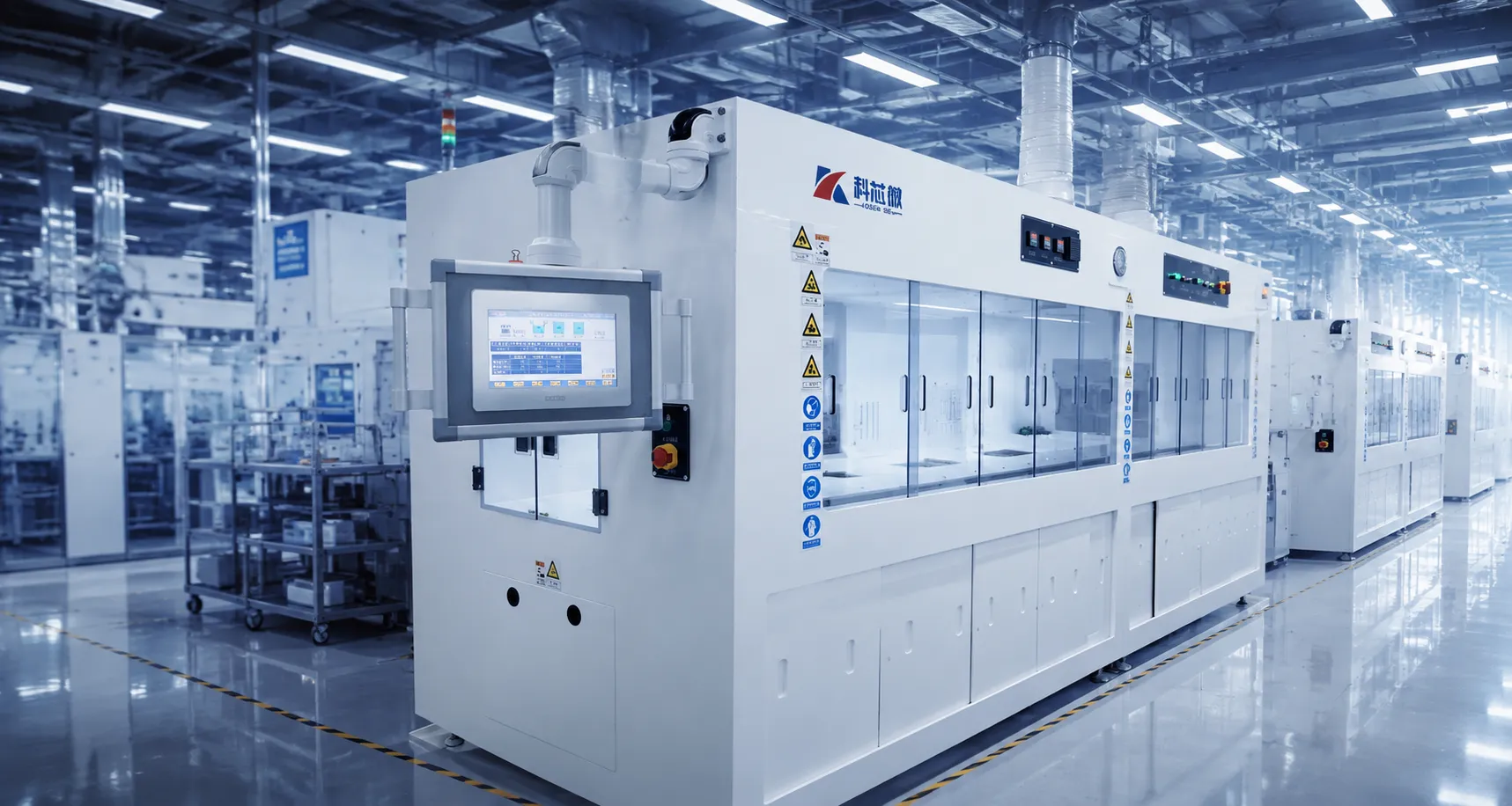
Field-tested and qualified on active high-volume production lines worldwide.
Strict quality control protocols ensuring consistent manufacturing and operation.
Precision fluid delivery systems built for ultra-clean, defect-free chemical processing.
Field Performance Metrics & Yield Improvement Proof
KOSEN SEMI wet process systems deliver high throughput and maximum yield for global wafer fabs through stringent contamination control and unmatched Engineering Capability.
Quantified yield enhancement verified across advanced node wafer manufacturing lines.
Ultra-high chemical purity standards safeguarding wafers from micro-scale metallic impurities.
Proven operational stability for continuous, 24/7 high-volume fab manufacturing cycles.
Successful wet bench and wafer cleaning systems installations in Tier-1 fabs worldwide.
Production Line Performance Validation
Empirical telemetry and process log data across multi-site fab deployments demonstrate repeatable defect reduction, superior uptime, and minimized total cost of ownership, especially with our Single Wafer Cleaning Systems.
- Automated chemical recirculation with precise temperature and micro-bubble control
- Fully compliant with international SEMI S2, S8, and CE cleanroom standards
- Inline real-time particle tracking paired with predictive maintenance telemetry
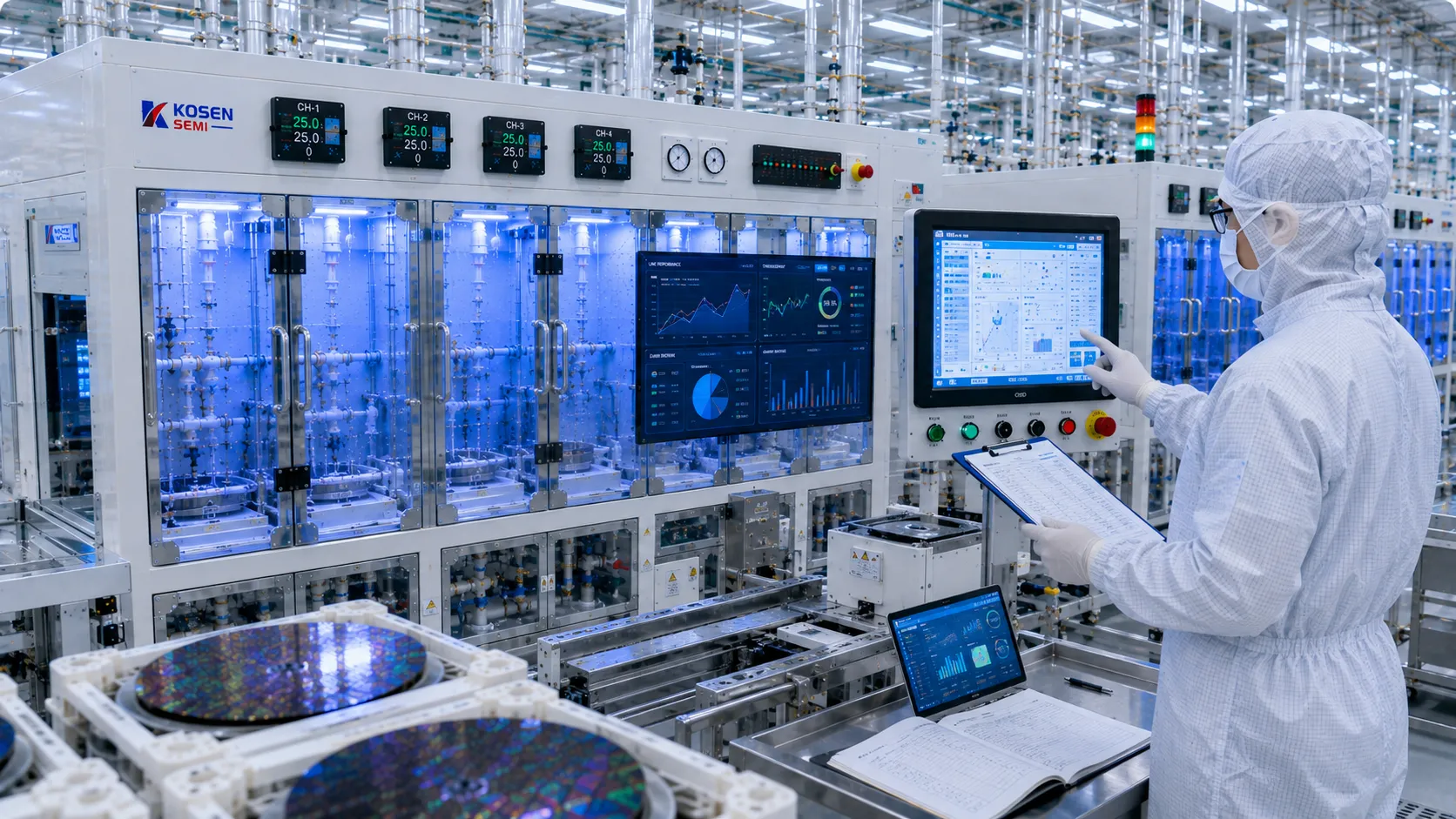
Featured Case Studies: Proven Wet Bench & Wafer Cleaning Success
KOSEN SEMI delivers field-proven wet bench installation and wafer cleaning systems upgrade solutions across leading semiconductor manufacturing facilities worldwide. Each featured case study below documents real-world fab challenges, custom wet process engineering, and rigorously verified yield outcomes—providing procurement directors and process engineering teams with the empirical evidence needed to evaluate tool performance for their own production lines.
From 300mm advanced logic foundries scaling wafer throughput to power device manufacturers controlling 200 nm-class particle defects, with optimized capability down to 100 nm, these semiconductor case studies reflect the operational reliability of KOSEN SEMI's custom wet bench solutions. Use the category filters below to explore case studies by equipment installation type or process application.
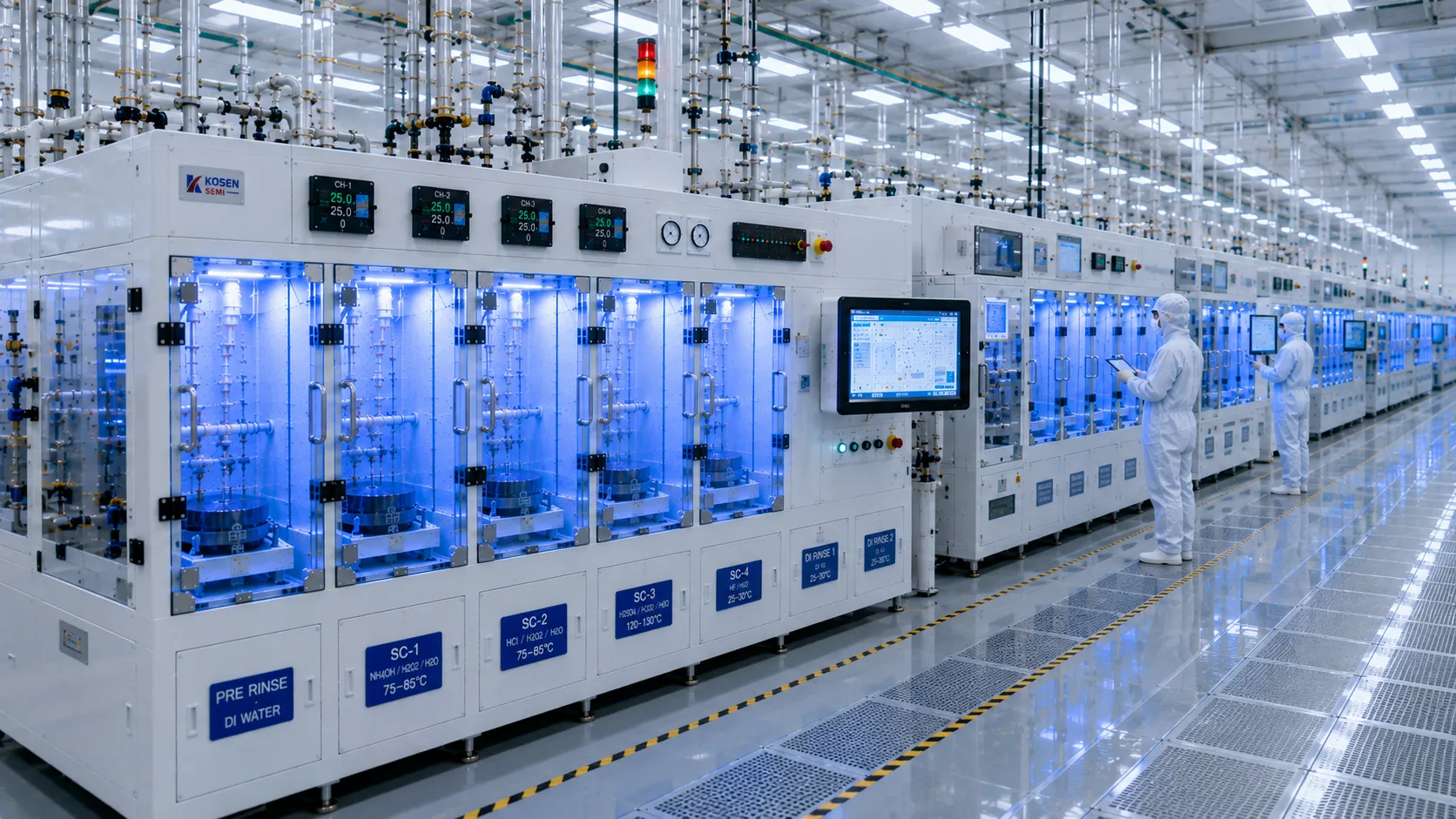 Wet Bench Installation
 Fully Automated Wet Bench Installation — 300mm Logic Fab
- Customer Background: High-volume 300mm logic semiconductor fab seeking to eliminate capacity bottlenecks in FEOL/BEOL wet etch and cleaning modules. Learn more about our customer success initiatives.
- Deployed Product: KOSEN SEMI Fully Automated Wet Bench with integrated chemical recirculation, megasonic agitation, and real-time process monitoring.
- Core Challenge: Legacy semi-automated wet stations generated high wafer handling variability, micro-particle defects, and unacceptable chemical consumption.
- Verified Result: +25% Throughput Increase with a 35% reduction in chemical bath turnover within 90 days of qualification.
KOSEN SEMI field engineers managed turn-key cleanroom installation, software integration with the fab's MES, and Site Acceptance Testing (SAT) inside ISO Class 5–7 cleanroom environments, delivering rapid ramp velocity without causing unplanned production downtime.
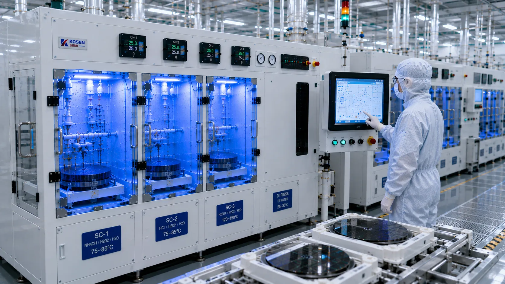 Wafer Cleaning Upgrade
 Single-Wafer Cleaning Upgrade — Power Semiconductor Fab
- Customer Background: Discrete power device manufacturer experiencing 200 nm-class particle contamination, with optimized evaluation down to 100 nm impacting final die yield on SiC/Si lines.
- Deployed Product: KOSEN SEMI Single-Wafer Cleaning Upgrade featuring multi-frequency megasonic nozzles and closed-loop chemical dispensing. Explore our complete line of semiconductor products.
- Core Challenge: Conventional batch cleaning methods failed to clear 200 nm-class particulate residues, with optimized removal down to 100 nm from high-aspect-ratio trench structures prior to gate oxidation.
- Verified Result: 40% Reduction in Particle Defect Rate verified via inline optical defect inspection post-deployment.
Delivered as a drop-in equipment retrofitting solution with minimal line interruption, KOSEN SEMI process engineers optimized recipe dynamics to satisfy stringent automotive-grade quality standards.
RCA Cleaning Chemistry Optimization — CMOS Foundry
- Customer Background: Leading CMOS foundry requiring advanced surface contamination control while lowering chemical consumption in pre-gate oxide cleans.
- Solution: KOSEN SEMI RCA sequence optimization utilizing ultra-dilute SC-1/SC-2 chemistry modules and real-time inline metal ion tracking.
- Verified Result: <0.005 ppb Metal Contamination achieved across continuous volume runs; chemical consumption decreased by 32%.
By refining fluid dynamics and chemical dosing precision, KOSEN SEMI helped this fab achieve ITRS-compliant substrate purity while significantly lowering hazardous chemical disposal overhead.
Scrubber System Retrofit & Bench Modernization — Advanced Packaging
- Customer Background: Advanced packaging facility requiring scrubber hardware modernization to handle post-grind and redistribution layer (RDL) cleans.
- Solution: KOSEN SEMI modular scrubber integration retrofitted into existing wet bench architecture with dual-brush modules and high-pressure DIW rinsing.
- Verified Result: 99.8% Tool Uptime sustained post-retrofit with reduced slurry particle redeposition over 12 months.
Executed during a scheduled facility turnaround window, this wet bench installation upgrade preserved production continuity while elevating post-dicing clean capabilities for advanced 2.5D/3D packaging lines.
Why Procurement & Fab Engineering Teams Reference KOSEN SEMI Case Studies
Every featured case study in this hub is anchored in direct fab-site data—not idealized laboratory projections. Yield improvement metrics, defect reduction percentages, and tool availability figures are compiled from customer-accepted Site Acceptance Testing (SAT) sign-offs and post-installation production logs. KOSEN SEMI provides customized wet bench installation and wafer cleaning upgrade solutions engineered to align with the specific process windows and chemical constraints of receiving semiconductor fabs.
- All operational outcomes are verified through customer SAT sign-off and inline metrology inspection.
- Projects span 200mm and 300mm logic fabs, compound semiconductor foundries (SiC/GaN), and advanced packaging lines.
- KOSEN SEMI field engineers remain on-site through production ramp to guarantee sustained tool stability.
- Detailed technical dossiers—including process recipes, equipment specs, and defect reduction curves—are available under NDA for qualified evaluation.
Semiconductor Wet Process Applications & Equipment Matrix
From advanced silicon integrated circuits to compound semiconductors, KOSEN SEMI delivers custom wet bench solutions engineered to meet demanding fab process windows. Backed by our dedicated focus, learn more about-us and our core competencies.
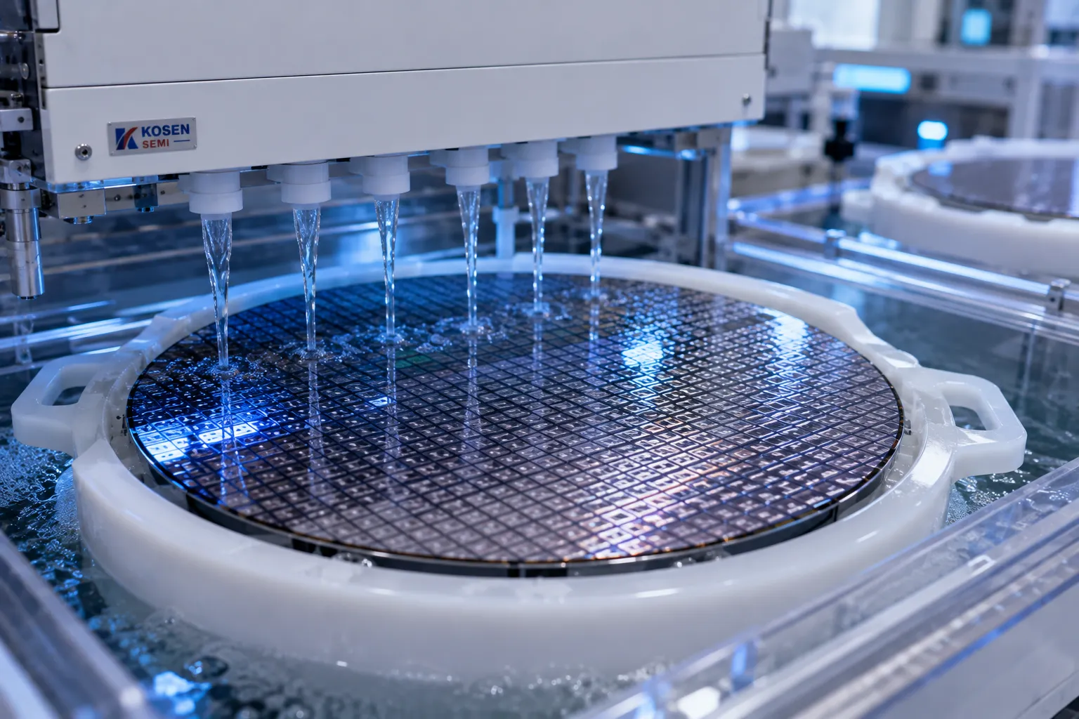
Front-End-of-Line (FEOL)
High-precision wet chemical processing for advanced silicon wafer fabrication, delivering rigorous defect reduction and uniform surface preparation.
Applicable Process Scenarios
- Anisotropic wet etching for fine circuit patterns
- High-selectivity chemical photoresist stripping
- Ultra-clean RCA surface contamination control using advanced wafer-cleaning-systems
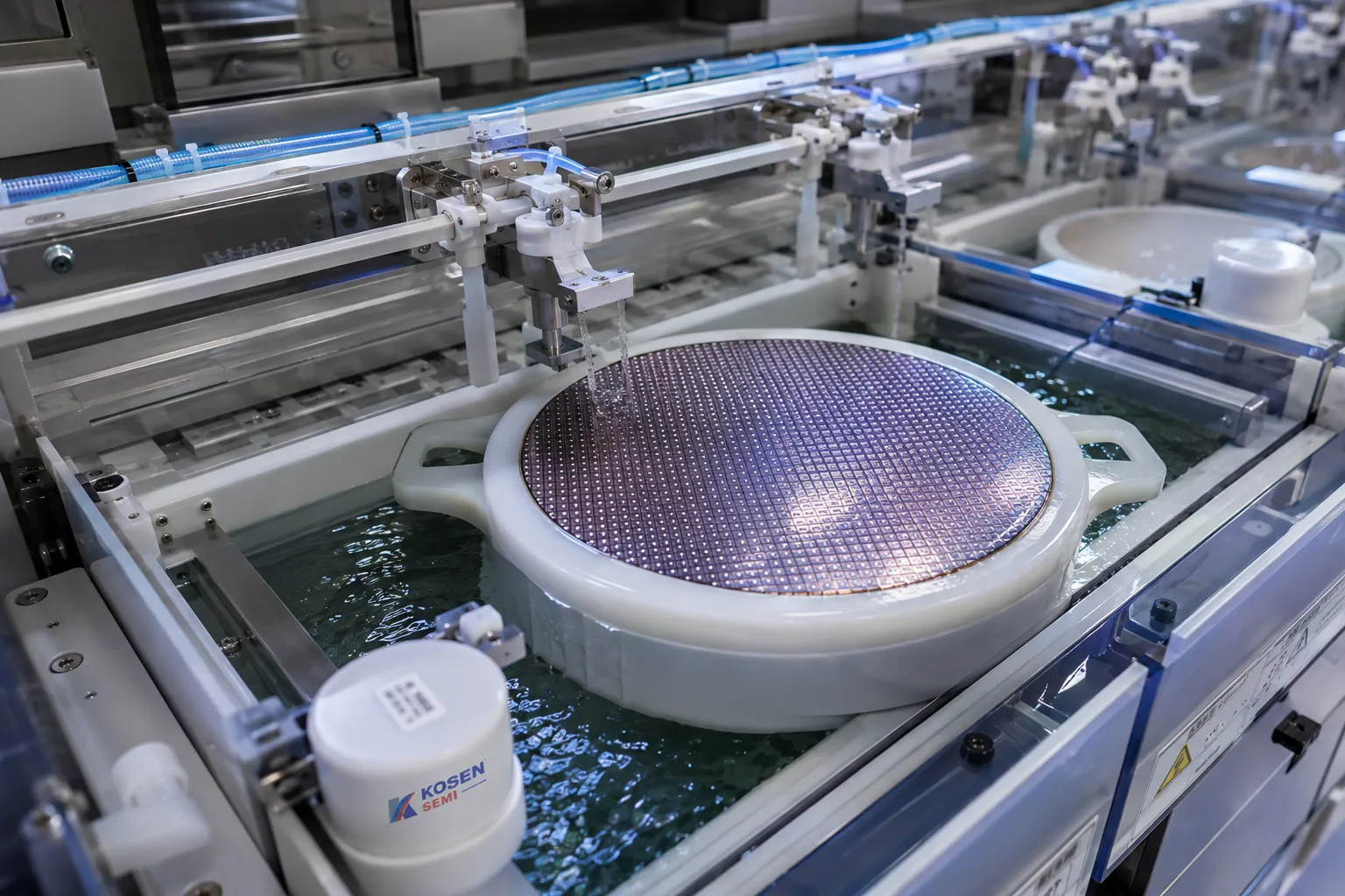
Back-End-of-Line (BEOL)
Automated wet processing tailored for advanced packaging lines, supporting defect-free wafer bumping and post-etch residue removal.
Applicable Process Scenarios
- Automated wafer bumping pre-treatment
- Post-etch copper cleaning with Single Wafer Cleaning Systems for residue removal
- Substrate surface preparation for 2.5D/3D IC packages
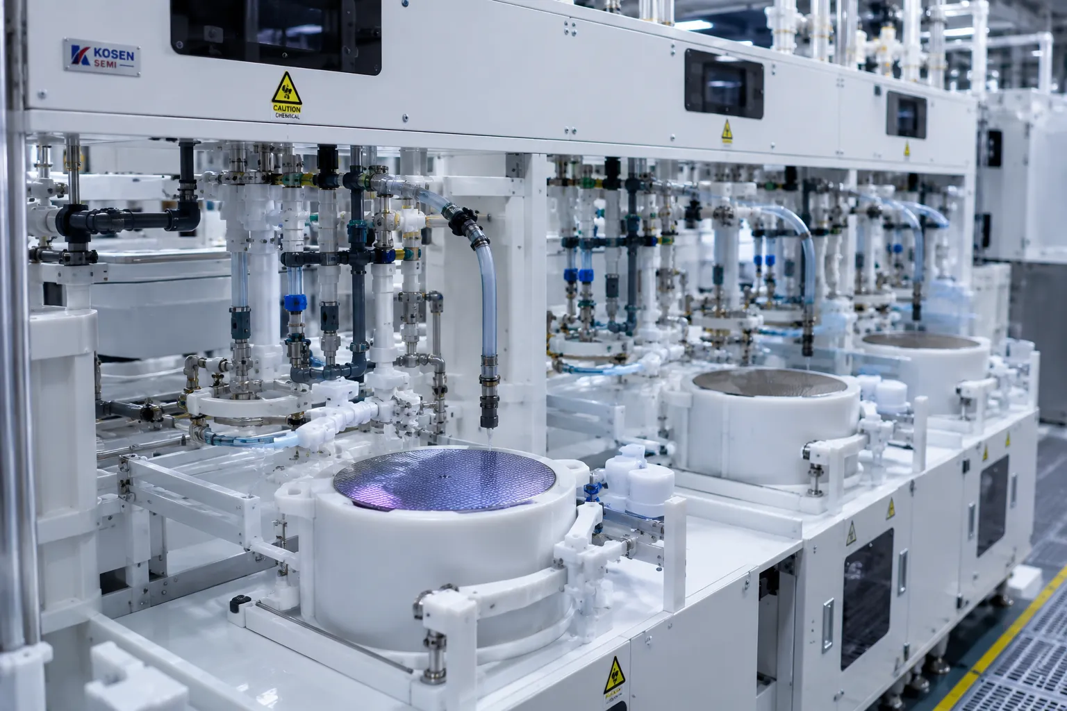
Compound Semiconductors
Custom wet bench solutions optimized for wide-bandgap materials, enabling stable chemical delivery for high-power device fabrication.
Applicable Process Scenarios
- Custom wet bench systems for SiC substrate cleaning
- Selective chemical etching for GaN power devices
- High-temperature acid processing for power chips
Semiconductor Client Success Stories & Rigorous Fab Validation Process
From initial process modeling to high-volume manufacturing ramp, KOSEN SEMI delivers fully transparent, risk-mitigated wet process solutions. Our semiconductor client success stories showcase how our engineering teams collaborate directly with fab leadership through every stage of our standardized fab validation process—ensuring rapid tool qualification, seamless SECS/GEM integration, and guaranteed yield performance.
Process Evaluation & Cleaning Chemistry Simulation
Every deployment begins with comprehensive chemical-surface interaction modeling and recipe feasibility testing. KOSEN SEMI engineers evaluate substrate topography, surface energy, and contaminant properties to establish precise fluid dynamics, megasonic energy distribution, and chemical ratios required for advanced wafer cleaning systems and 200 nm defect reduction, with optimized capability down to 100 nm.
- ✓ Computational Fluid Dynamics (CFD): Optimizes chemical flow velocity and boundary-layer stripping across 200mm and 300mm wafers.
- ✓ Chemistry & Substrate Compatibility: Verifies etch selectivities and zero surface degradation prior to full-scale build.
Custom Equipment Engineering & Cleanroom Manufacturing
Our specialized cleanroom manufacturing facility fabricates custom automated wet benches and single wafer cleaning systems engineered for exact fab floor plan constraints. We integrate high-purity fluoropolymer fluid lines, fire-suppression systems, and corrosion-resistant enclosures.
- ✓ ISO Class 5–7 Cleanroom Assembly: Prevents airborne particle contamination during mechanical construction and wiring.
- ✓ Modular Architecture: Streamlines cleanroom installation, minimizes footprint, and shortens utility hookup timelines.
On-Site Installation, SECS/GEM Integration & SAT Qualification
KOSEN SEMI field service engineers manage facility connections, exhaust balancing, chemical manifold tie-ins, and communication protocols. As a core component of our fab validation process, formal Site Acceptance Testing (SAT) verifies defectivity targets and operational uptime.
- ✓ SECS/GEM Automation Protocols: Ensures real-time recipe execution, tool telemetry, and MES integration.
- ✓ Particle & Contamination Audit: Validates 200 nm particle specifications, with optimized evaluation down to 100 nm and ultra-low metallic residue tolerances.
High-Volume Manufacturing Ramp & Yield Optimization
Our partnership extends long past initial sign-off. KOSEN SEMI provides dedicated field support through mass production ramp-up, continuously optimizing chemical consumption, monitoring filter life, and analyzing statistical process control data for yield stability.
- ✓ Dedicated Field Support: On-site engineering coverage and rapid response times for continuous uptime.
- ✓ Statistical Process Control (SPC): Ongoing data monitoring to ensure long-term process repeatability and yield growth.
"KOSEN SEMI demonstrated outstanding technical execution during our 300mm wafer fab expansion. Their field service engineers completed cleanroom hookup, SECS/GEM validation, and SAT qualification two weeks ahead of schedule, enabling us to hit volume targets without material yield disruption."
Director of Wet Process Engineering
Tier-1 300mm Advanced Semiconductor Fab
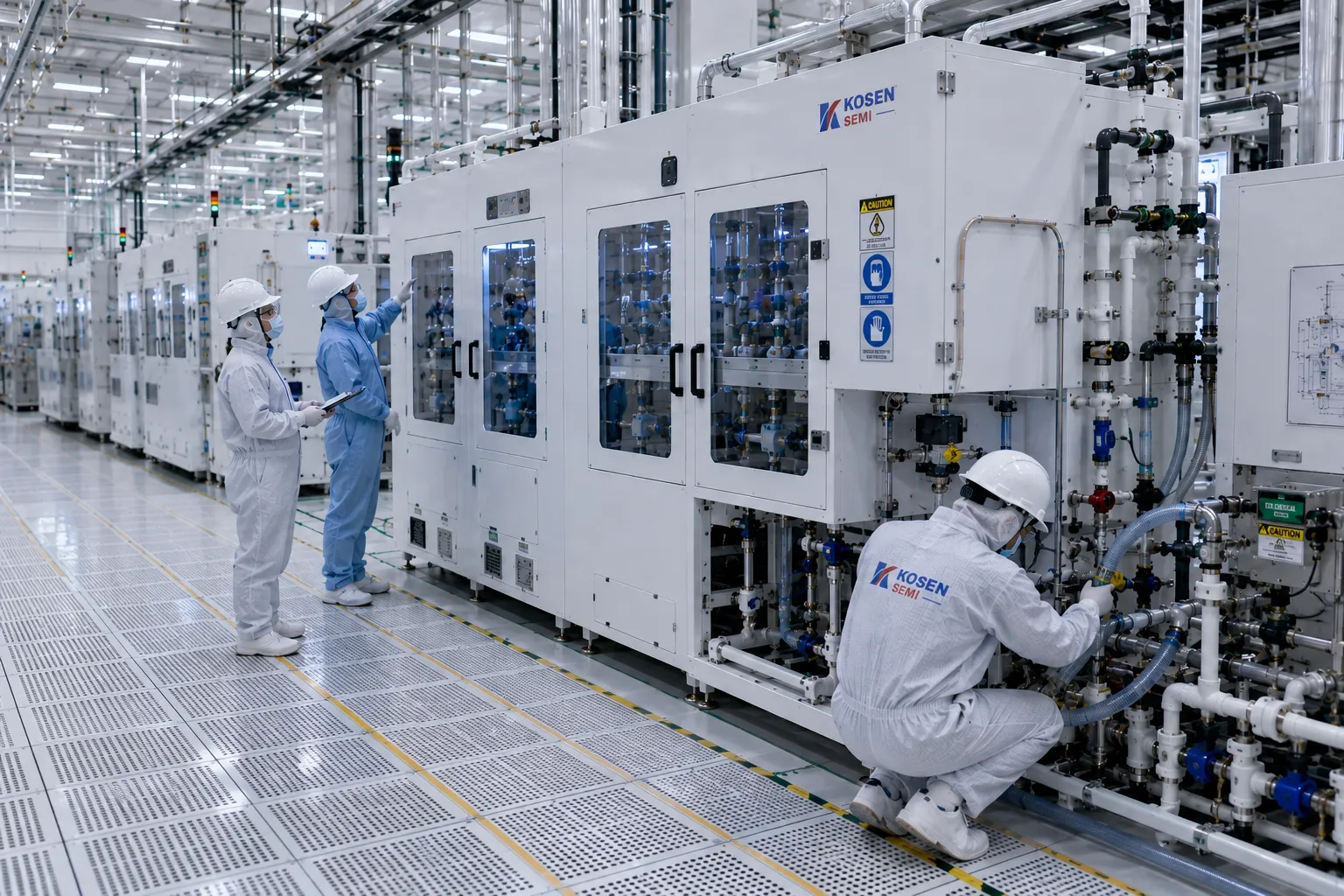
Proven On-Site Fab Integration
Our certified engineering teams manage end-to-end tool rigging, chemical hookups, and exhaust balancing in compliance with strict ISO cleanroom standards.
"Upgrading our compound semiconductor wet bench line was smooth and predictable. The KOSEN SEMI team tailored the chemical delivery system directly to our cleanroom geometry, generating an immediate 18% reduction in chemical consumption and minimized unplanned downtime."
VP of Fab Operations
Compound Semiconductor Manufacturer
Cleaning Equipment Installation & Deployment FAQ
Procuring high-precision wet process equipment and executing cleanroom upgrades requires technical validation, predictable delivery schedules, and verified performance guarantees. KOSEN SEMI addresses critical procurement and cleaning equipment installation questions by providing transparent empirical data, customized engineering workflows, and pre-installation laboratory testing to eliminate operational risks for semiconductor fabrication facilities worldwide.
Every yield enhancement metric published in KOSEN SEMI case studies originates from empirical wafer fab production data collected over extended operational windows. Prior to equipment integration, baseline yield loss, surface defect density, and particle levels are documented across a minimum of 1,000 consecutive production wafers.
Post-installation performance is verified using automated optical inspection (AOI) systems and total reflection X-ray fluorescence (TXRF) spectroscopy. Surface particle counts are verified at 200 nm thresholds, with optimized evaluation down to 100 nm, ensuring metallic contamination levels stay strictly below <0.005 ppb. die-level parametric yield improvements are independently calculated and signed off by client fab engineering supervisors.
- Inline particle defect counting before and after RCA cleaning cycles
- TXRF spectroscopy for trace surface metal contamination analysis
- Statistical process control (SPC) analysis across multiple wafer lots
Equipment Deployment Standards
| Deployment Parameter | Standard Benchmark |
|---|---|
| Metal Contamination Standard | <0.005 ppb Threshold |
| System Uptime Guarantee | 99.8% Availability |
| Upgrade Installation Window | 48 to 72 Hours |
| Custom Equipment Lead Time | 16 to 24 Weeks |
| Lab Demo Trial Capabilities | SiC, GaN, RCA & PR Strip |
Technical Risk Mitigation Support
KOSEN SEMI offers comprehensive technical Q&A, process validation reports, and preliminary laboratory demo testing to help semiconductor manufacturers eliminate procurement decision risks and accelerate fab-qualified deployment.