
Knowledge Center, Technical Articles, and Buyer Support FAQ
KOSEN SEMI organizes decades of semiconductor wet equipment R&D experience into a one-stop knowledge exploration hub for all users.
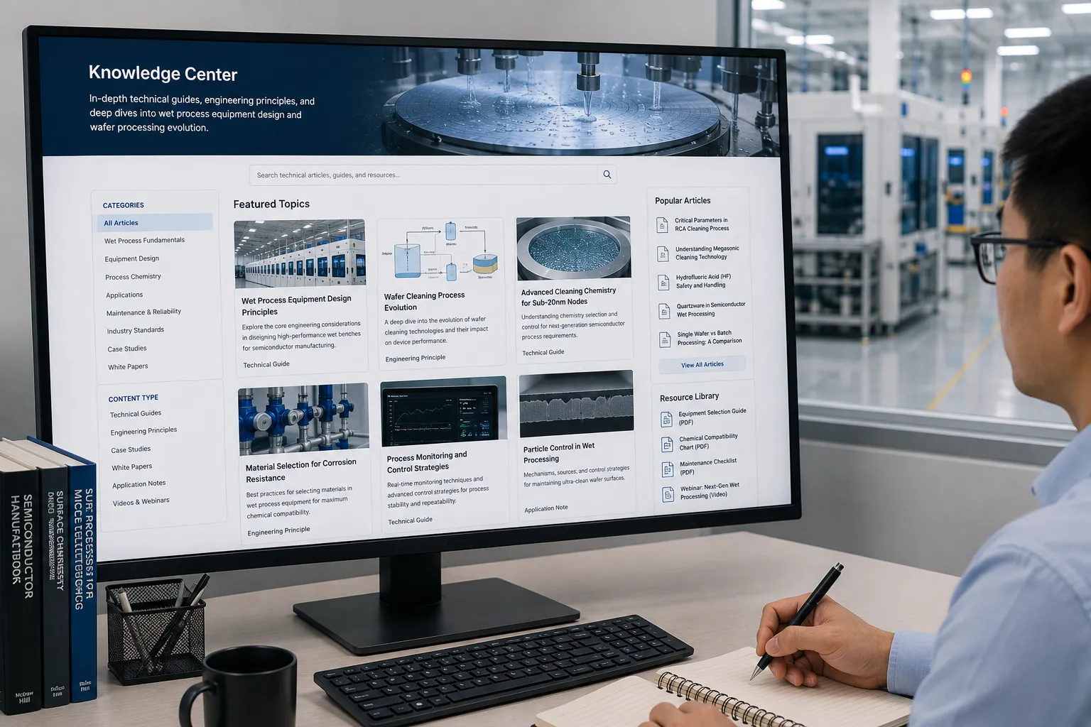
Knowledge Center
In-depth technical guides, engineering principles, and deep dives into wet process equipment design and wafer processing evolution.
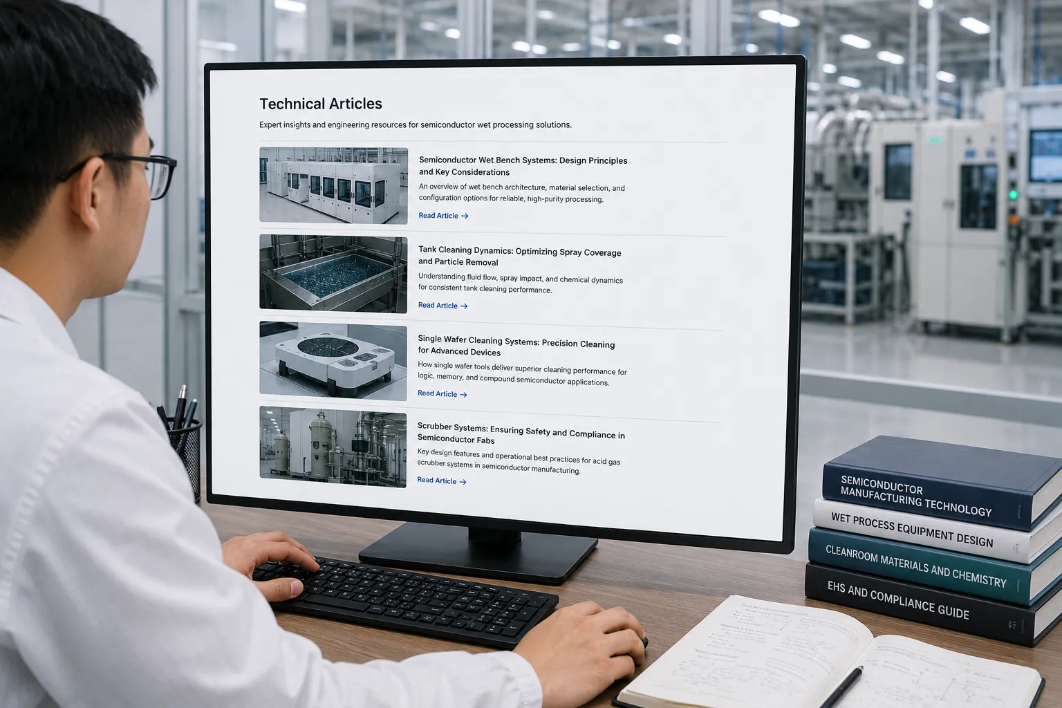
Technical Articles
Expert articles covering semiconductor wet benches, tank cleaning dynamics, Single Wafer Cleaning Systems, and scrubber systems.
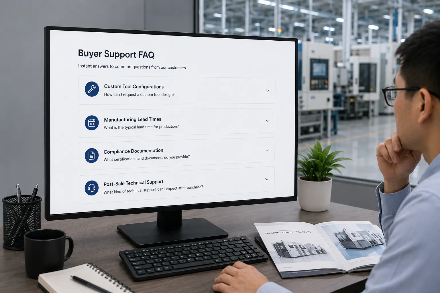
Buyer Support FAQ
Instant answers regarding custom tool configurations, manufacturing lead times, compliance documentation, and post-sale technical support.
Frontier Exploration of Semiconductor Wet Processes and Equipment Technology
Access peer-reviewed engineering analyses, semiconductor wet bench documentation, and wet process technology insights curated by KOSEN SEMI experts to eliminate contamination, optimize wafer yield, and streamline cleanroom integration.
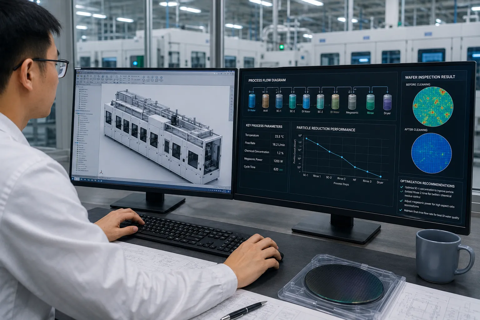
Advanced Wafer Cleaning System Engineering & Process Optimization
KOSEN SEMI supports wafer cleaning projects involving RCA cleaning sequences, chemical concentration management, megasonic cleaning, drying processes, contamination control, and customized equipment configuration according to specific wafer and production requirements.
Engineering Focus
- Wafer cleaning sequence and chemical process configuration.
- Megasonic cleaning, rinsing, drying, and contamination control.
- Equipment configuration based on wafer size, throughput, and fab requirements.
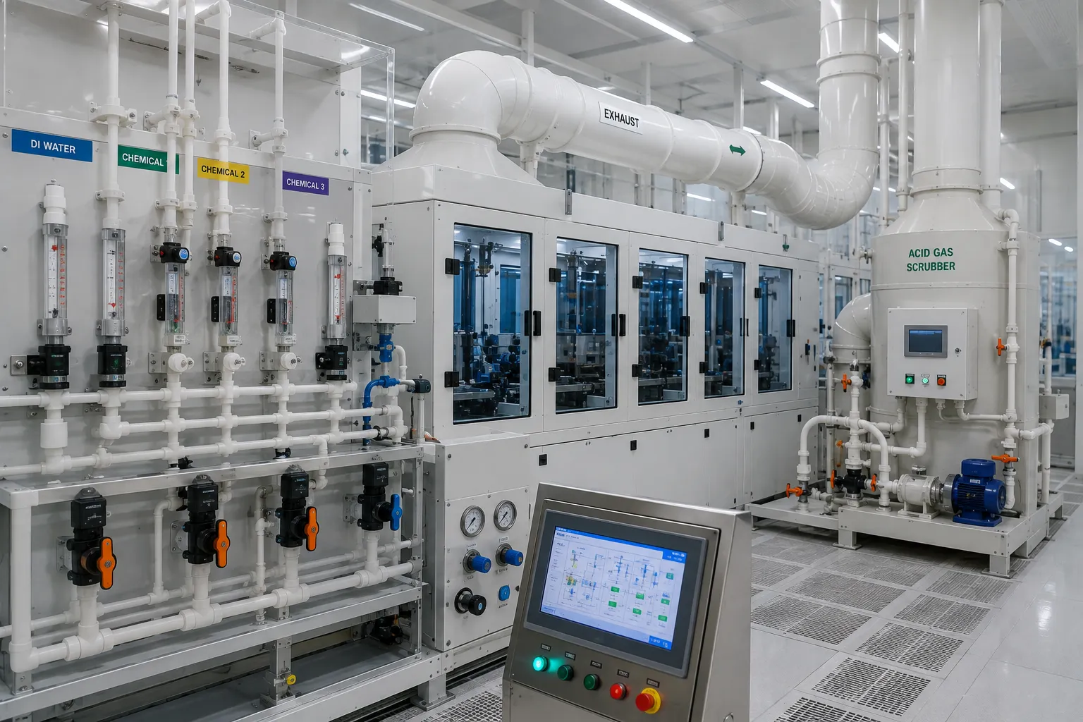
Semiconductor Wet Bench Fluidics & Exhaust Integration
Discuss bath circulation, high-purity chemical piping, exhaust configuration, material selection, process tanks, and automated chemical handling requirements.
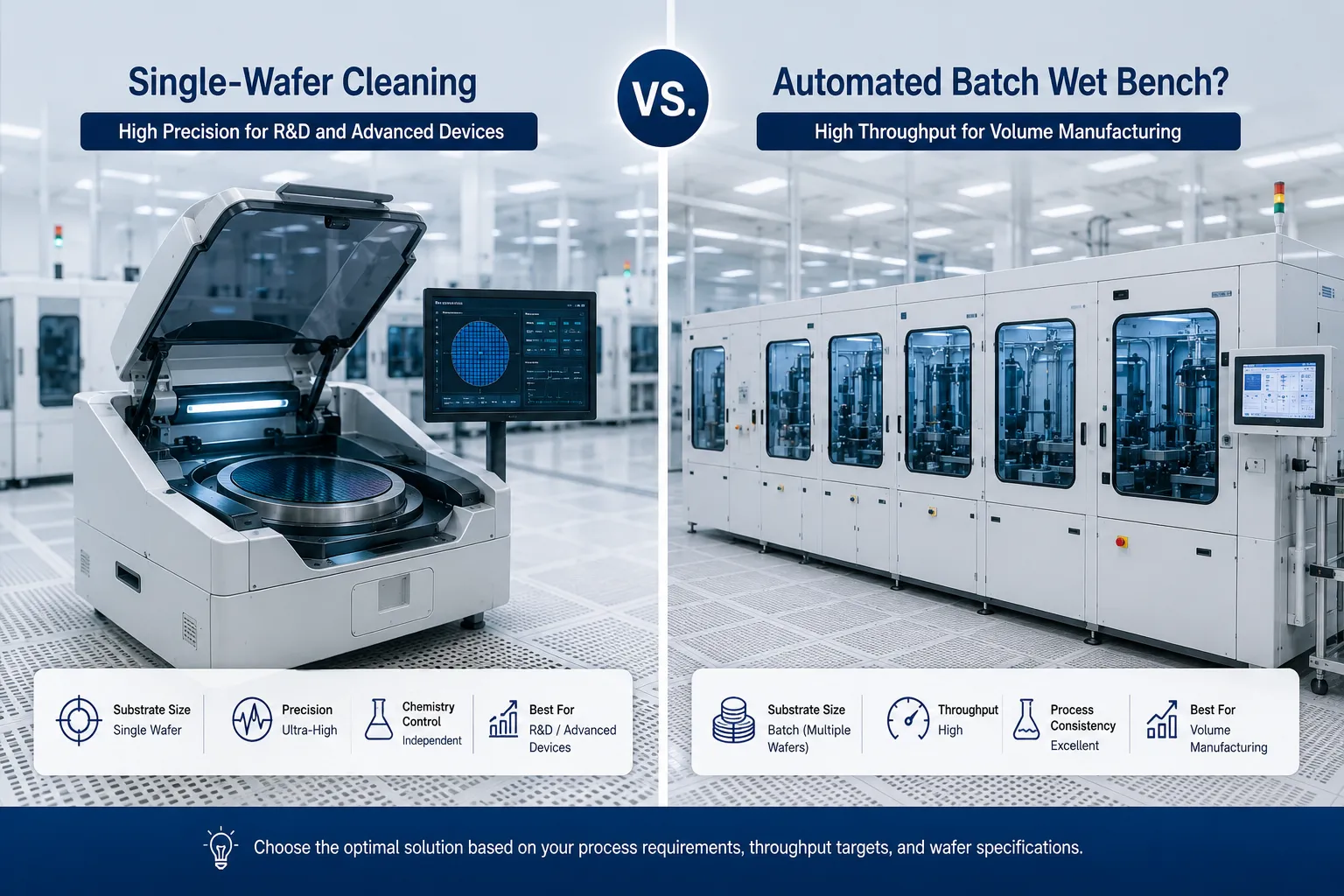
Single-Wafer Cleaning or Automated Batch Wet Bench?
Our team can review wafer size, process sequence, chemical usage, throughput, automation level, and contamination-control requirements to help define a suitable system architecture.
Wet Process Technology Insights for Modern Wafer Fabrication
Selecting the optimal wet processing architecture is fundamental to minimizing defect density and elevating overall wafer throughput. KOSEN SEMI designs custom chemical distribution manifolds, precise thermal control systems, and specialized agitation mechanisms tailored to demanding fab requirements. Below is a detailed technical comparison of the primary wet cleaning equipment paradigms used in advanced semiconductor facilities.
| Equipment Architecture | Primary Application | Particle Removal Efficiency | Throughput Capacity | Key Advantage |
|---|---|---|---|---|
| Automated Batch Wet Bench | High-volume wafer stripping, chemical etching, and pre-diffusion cleaning | Standard control at 200 nm; optimized to 100 nm | Very High (50–100 wafers/batch) | Lowest chemical and consumable cost per wafer |
| Single-Wafer Cleaning Systems (Spin Cleaners) | Critical gate clean, post-CMP, and 200 nm standard / 100 nm optimized processing | 200 nm standard; 100 nm optimized | Moderate (Multi-chamber parallel processing) | Minimized cross-contamination risk between individual wafers |
| Scrubber Systems | Post-grinding, wafer backside cleaning, and soft mechanical particle scrub | High for physical particulate matter | High continuous line throughput | Superior mechanical slurry & residue removal |
Frequently Asked Questions on Equipment Procurement and Technical Support
Navigating semiconductor wet bench specifications, cleanroom integration requirements, and manufacturing delivery timelines requires absolute engineering clarity. KOSEN SEMI provides transparent procurement workflows and comprehensive technical consultation—addressing your core semiconductor equipment FAQ needs and providing dedicated customization & lead times support from initial tool selection through high-volume wafer production.
01 What are the standard manufacturing lead times for KOSEN SEMI wet processing benches and automated cleaning tools?
Standard wet processing tools, manual wet benches, and modular cleanroom chemical delivery units typically feature lead times of 8 to 12 weeks following final engineering design sign-off. For fully customized Single Wafer Cleaning Systems or high-throughput batch wet processing equipment, manufacturing lead times range between 16 to 24 weeks, depending on chemical delivery complexity, inline metrology requirements, and recipe customization.
Our structured customization & lead times support framework encompasses rigorous 3D CAD modeling, component fabrication, cleanroom sub-assembly, Factory Acceptance Testing (FAT), and international logistics staging. KOSEN SEMI maintains an expedited inventory of critical pumps, valves, and PLC controllers to offer fast-track manufacturing slots for urgent fab expansions.
01 How does the custom wet bench engineering and workflow validation process operate?
Custom wet bench engineering follows a transparent four-stage milestone sequence tailored to specific wafer substrate dimensions (100mm to 300mm), throughput goals, and aggressive chemical process requirements:
- Requirement Audit & Specification: Comprehensive analysis of targeted etch rates, surface particle cleanliness limits, chemical delivery logistics, and cleanroom footprint boundaries.
- 3D CAD Design & Fluid Modeling: Advanced computational fluid dynamics (CFD) simulation utilizing our advanced Engineering Capability to optimize bath fluid dynamics, chemical recirculation, and exhaust extraction efficiency.
- Factory Acceptance Testing (FAT): Complete hardware qualification, dry cycle testing, and chemical sequence verification conducted inside our ISO-certified cleanroom facility.
- Site Acceptance Testing (SAT): On-site equipment positioning, utility hookup to facility Ultra-Pure Water (UPW) lines, chemical distribution integration, and final process handover.
03 What safety, environmental, and cleanroom standards do KOSEN SEMI systems meet?
Every piece of wet equipment built by KOSEN SEMI adheres strictly to international semiconductor manufacturing safety and quality standards. All systems carry full CE certification, ISO 9001 quality management compliance, and comply with SEMI S2 (Environmental, Health, and Safety) and SEMI S8 (Ergonomic Engineering) guidelines.
To eliminate fire hazards associated with volatile solvent cleaning, tool cabinets are constructed using FM4910-approved fire-retardant polymers (such as PVDF and polypropylene). Furthermore, all tools are engineered for seamless operation within ISO Class 5–7 cleanroom environments, reducing particulate contamination risk during critical wafer processing steps.
04 What post-sale technical support and global field service guarantees are provided?
KOSEN SEMI backs every tool installation with a standard 12-month comprehensive warranty, extendable up to 36 months via customized Service Level Agreements (SLAs). Our dedicated team addresses all wet bench support questions through 24/7 remote engineering assistance, rapid Field Service Engineer (FSE) dispatch, and OEM spare parts availability guaranteed within 48 hours across major global semiconductor fabrication hubs.
Preventative maintenance protocols, operator safety certification training, and continuous process optimization assessments are included with every commercial procurement contract to ensure maximum tool uptime, high yield stability, and process repeatability.
05 How do wetted materials support chemical compatibility and 200 nm standard / 100 nm optimized particle removal?
Wetted components, chemical plumbing paths, and fluid manifolds are constructed exclusively using ultra-high-purity fluoropolymers such as PFA, PVDF, PTFE, and high-purity quartz. Whether running concentrated HF, SPM (Piranha), SC-1, SC-2, or organic solvents in our semiconductor-wet-bench-systems, wetted materials undergo stringent leaching evaluations to protect against metallic and ionic contamination.
Integrated multi-frequency megasonic transducers, point-of-use (POU) chemical filtration, and surface-tension-driven N2 Marangoni drying options support particle removal at 200 nm standard capability, optimized down to 100 nm, supporting yield protection across silicon, SiC, and GaN wafer fabrication lines.
Question Not Found?
Every semiconductor wet processing line carries unique chemical recipes, throughput targets, and cleanroom constraints. Speak directly with our application engineers for tailored equipment consultation and wet bench support questions.
Semiconductor Wet Process Resources
Access our central technical guidance hub for in-depth wet bench documentation, product specifications, whitepapers, and cleanroom integration manuals.
Request Wet Process Equipment Technical Documentation
KOSEN SEMI provides technical documentation to support semiconductor equipment evaluation, project planning, facility integration, and supplier qualification. Available information may include equipment specifications, process configuration details, utility requirements, layout information, and other project-related technical materials.
Contact our engineering team with your process and equipment requirements. We will review your application and provide the relevant available documentation for your project.
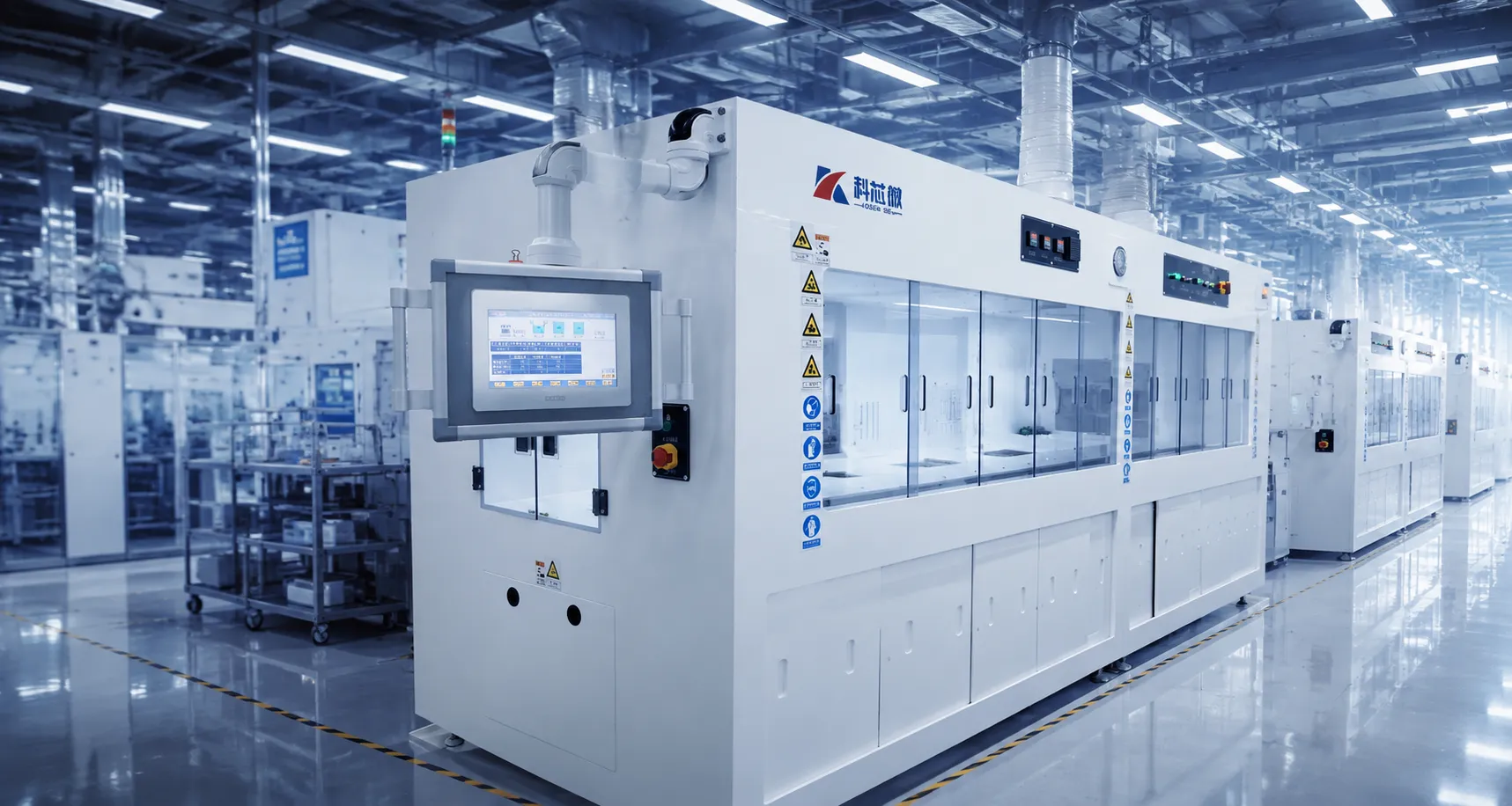
Wafer Cleaning Process & Equipment Documentation
Request available technical information for wafer cleaning systems, including process configuration, chemical handling, cleaning sequence considerations, utility requirements, equipment layout, and project-specific integration details.
Available Information May Include
- Wafer cleaning process configuration and equipment architecture
- Chemical delivery, rinsing, drying, and process-control information
- Equipment layout and utility requirements based on project configuration
Wet Bench & Scrubber Technical Specifications
Request technical information for KOSEN SEMI wet benches and semiconductor scrubber systems, including dimensional information, facility interfaces, utility connections, materials, exhaust configuration, and automation options relevant to your project.
Specification Topics
- Equipment dimensions and installation footprint information
- Chemical, exhaust, power, water, and facility utility requirements
- Automation and system integration information according to equipment scope
Technical Documentation Available for Project Evaluation
Semiconductor wet processing equipment is typically configured around the customer’s process flow, facility conditions, wafer requirements, and automation scope. KOSEN SEMI therefore provides technical information based on the specific project rather than relying on generic downloadable documents.
| Technical Resource | Availability | Primary Audience | Key Focus |
|---|---|---|---|
| Wafer Cleaning Process Documentation | On Request | Process Engineers | Cleaning process & configuration |
| Wet Bench Technical Specifications | Project-Based | Facility & Procurement Teams | Utilities, dimensions & integration |
| Scrubber System Specifications | Project-Based | Facility & EHS Teams | Exhaust & system configuration |
Typical Documentation Topics
- Equipment configuration and installation footprint
- Utility, chemical, exhaust, and facility interface requirements
- Process-related and integration information relevant to the selected equipment
Need Custom Engineering Specifications?
If your project requires tailored tank configurations, chemical delivery modules, custom wet processing equipment, or exhaust scrubber integration, send us your requirements for technical review.
Contact KOSEN SEMI