
Semiconductor Wet Process Knowledge Center & Technical Guides
KOSEN SEMI empowers semiconductor fab engineers, process integration specialists, and packaging teams with authoritative technical resources. Learn more about us and explore engineering-grade guides covering wafer cleaning systems, automated wet bench configurations, fluoropolymer compatibility, and exhaust scrubber compliance.
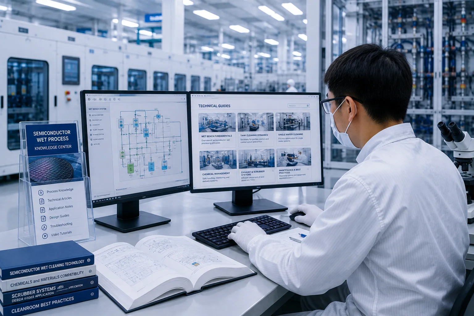
Explore Wet Process Categories & Equipment Selection Guides
Navigating semiconductor wet process architectures requires a rigorous understanding of chemical kinetics, surface contamination mechanics, and hardware scalability. Built upon KOSEN SEMI's extensive R&D in custom wet process systems and our advanced Engineering Capability, these structured technical guides simplify complex equipment sourcing logic. Explore our core category nodes below to evaluate wet process fundamentals, review in-depth semiconductor articles, and navigate precise equipment selection for your fabrication facility.
Wet Process Fundamentals & Surface Chemistry
A foundational technical resource detailing chemical etching mechanisms, liquid-phase surface cleaning kinetics, and substrate wetting dynamics. This guide establishes core wet process fundamentals to help process engineers model chemical bath life, optimize fluid dynamics, and establish initial equipment sourcing frameworks.
- Chemical Etching: Isotropic vs. anisotropic chemical reaction mechanics and selectivity
- Surface Cleaning: Substrate passivation, surface wetting, and particulate detachment
- Equipment Selection: Sourcing logic aligning chemical compatibility with target throughput
Wafer Cleaning Systems & Megasonic Mechanics
Comprehensive semiconductor articles analyzing particle removal mechanisms at 200 nm standard capability, optimized down to 100 nm, precise chemical dosing ratios, and acoustic energy distribution. These technical guides cover engineered protocols for high-precision wafer-cleaning-systems, RCA clean sequences, megasonic boundary layer thinning, and defect mitigation across advanced node substrates.
- Particle Removal: 200 nm standard particle detachment, optimized down to 100 nm, with electrostatic re-deposition control
- Chemical Dosing: Automated concentration monitoring for SC-1, SC-2, and SPM chemical loops
- Megasonic Mechanics: Acoustic frequency and power tuning to eliminate pattern collapse
Wet Bench Selection & Throughput Optimization
An authoritative wet bench guide providing comparative engineering evaluations across manual, semi-automated, and fully automated wet processing equipment, including specialized Single Wafer Cleaning Systems. Evaluate chemical heating loops, filtration recirculation rates, and robotic handling to match wet bench architectures directly to fab throughput targets.
- Bench Architecture: Manual, semi-automated, and fully automated footprint trade-offs
- Throughput Models: WPH yield optimization, chemical bath lifecycle, and filter sizing
- Material Compatibility: Tank selection guidelines for PFA, PVDF, PP, and High-Purity Quartz
Point-of-Use Scrubber Systems & Environmental Safety
Technical equipment selection guides covering acid mist neutralization, caustic exhaust scrubbing, and cleanroom air pressure balancing. Learn how point-of-use scrubber systems integrate into wet bench exhaust manifolds to maintain strict environmental compliance and cleanroom safety.
- Exhaust Neutralization: Scrubbing efficiency models for corrosive gases and acid mist recovery
- Cleanroom Safety: Static pressure management, emergency extraction, and airflow balance
- Compliance Standards: Full alignment with international SEMI S2/S8 guidelines and safety codes
Need Guidance on Custom Wet Equipment Selection?
KOSEN SEMI's engineering team provides specialized technical consultations to help fab managers specify wet bench architectures, chemical delivery systems, and exhaust scrubbers tailored to exact process requirements.
Engineering Selection Frameworks & Wafer Cleaning Methodologies
Evaluating advanced semiconductor wet processing equipment requires precise technical alignment between chemical compatibility, throughput targets, particle contamination limits, and fab footprint constraints. KOSEN SEMI provides engineering-grade decision frameworks built on strict SEMI S2/S8 safety standards to assist process engineers, fab operators, and facility managers in selecting optimal wet bench configurations, advanced wafer cleaning systems, and compliant scrubber selection strategies for high-yield device manufacturing. Learn more about-us and how our technical expertise focuses on delivering state-of-the-art wet processing solutions.
Wet Bench vs. Single Wafer Cleaning Architecture
Choosing between continuous batch immersion and single wafer spin processing represents a foundational engineering decision in semiconductor wet processing. Batch immersion wet benches deliver unmatched wafer-per-hour (WPH) throughput and low chemical cost for high-volume manufacturing, whereas Single Wafer Cleaning Systems offer isolated chemical dispensation, rapid megasonic energy distribution, and minimal cross-contamination risks for leading-edge device nodes.
- ✓ Automated Wet Bench: Best suited for high-throughput batch wafer cleaning methods, minimizing chemical consumption per wafer across SPM, SC-1, SC-2, and HF etch lines.
- ✓ Single Wafer Processing: Tailored for critical front-end-of-line (FEOL) wafer cleaning methods demanding precise single-use chemistry delivery, uniform megasonic coverage, and swift surface drying.
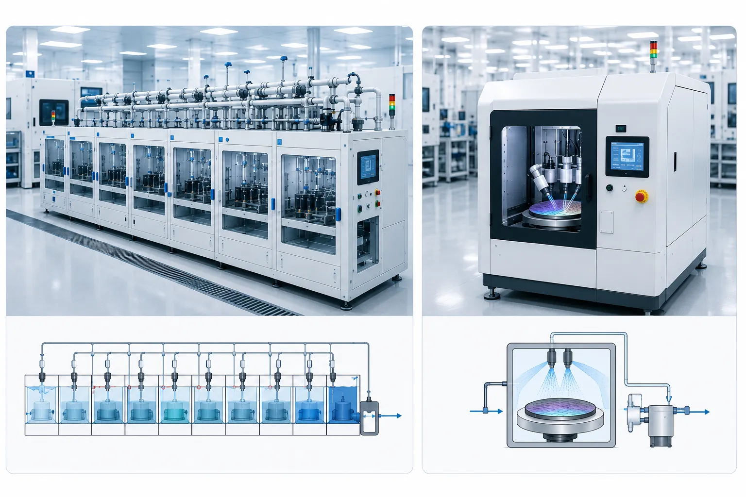
Equipment Performance & TCO Comparison Matrix
Comprehensive technical evaluation metrics for wet bench guide analysis, cleanroom utility sizing, and capital investment planning.
| Evaluation Parameter | Automated Immersion Wet Bench | Single Wafer Cleaning System | Engineering Recommendation |
|---|---|---|---|
| Throughput Capacity | High (200 – 400+ WPH depending on carrier/cassette batch size) | Moderate (30 – 80 WPH per multi-chamber process module) | Deploy automated wet benches for high-volume manufacturing (HVM) strip and clean steps. |
| Cross-Contamination Risk | Moderate (effectively controlled via quick-dump rinsing & continuous overflow design) | Low (minimized through single-use fresh chemical dispensing per wafer) | Single wafer systems are appropriate for 200 nm standard and optimized 100 nm gate preparation and sensitive contact cleans. |
| Cleanroom Footprint | Compact footprint per wafer processed (high volumetric efficiency) | Larger footprint needed for multi-chamber cluster tool configurations | Wet benches maximize WPH output per square meter of cleanroom floor space. |
| Chemical Consumption | High efficiency via inline bath recirculation, filtration & spike dosing | Higher chemical volume per wafer unless integrated with dedicated recovery loops | Recirculated wet bench chemical baths significantly lower ongoing consumable expenditures. |
| Total Cost of Ownership (TCO) | Lower capital investment and operational cost per processed wafer | Higher initial capital expenditure and elevated maintenance requirements | Wet bench architectures provide superior ROI for mature nodes, compound semis, and high-volume fabs. |
Chemical Compatibility & Tank Material Selection Guide
Selecting appropriate structural and tank materials prevents structural degradation, metallic leaching, and particle shedding during aggressive thermal acid, caustic alkali, and organic solvent process steps. KOSEN SEMI custom engineers wet bench systems using ultra-high purity fluoropolymers, specialized thermoplastics, and high-purity quartz matching specific process fluid thermodynamics.
| Material Type | Compatible Process Chemistries | Max Temp Limits | Key Physical Properties | Typical Process Application |
|---|---|---|---|---|
| PFA (Perfluoroalkoxy) | Hot SPM, Concentrated Acids, Organic Solvents, SC-1/SC-2 | Up to 180°C | Superior chemical inertness, zero trace metal leaching, exceptional flame resistance | High-temperature acid recirculating baths, chemical delivery manifold lines, and chemical injection valves |
| PVDF (Polyvinylidene Fluoride) | Ambient to Warm Acids, DI Water Lines, Ozone Systems | Up to 120°C | Outstanding mechanical strength, high abrasion resistance, broad chemical tolerance | Outer containment tanks, DI water overflow quick-dump rinsers, ambient acid/alkali etch baths |
| PP (NPP / Natural Polypropylene) | Alkaline Solutions, Mild Solvents, Low-Temp Acid Dilutions | Up to 80°C | High stress crack resistance, excellent structural rigidity, cost-effective formulation | Wet bench structural frame cabinets, secondary splash shields, alkali tanks, and exhaust manifolds |
| Quartz (High-Purity Fused Silica) | High-Temp Piranha (SPM), Nitric Acid (HNO3), Solvent Cleans | Up to 220°C | Extreme thermal shock tolerance, high optical purity, zero organic particle contamination | Quartz immersion baths, megasonic-assisted active tanks, thermal strip baths, and fast ramp heating units |
3-Step Interactive Equipment Selection Tree
Select your target wafer substrate dimensions, process chemistry requirements, and production volume to generate an immediate engineering recommendation tailored to your wet bench setup, process enclosure, and exhaust scrubber selection requirements.
Wafer Diameter
Process Chemistry
Production Scale
Fully Automated 200mm Wet Bench with PFA Baths & Integrated Acid Mist Scrubber
Fab Application Scenarios & Wet Process Solutions FAQ
KOSEN SEMI delivers high-precision wet process solutions engineered for complex, high-yield fab manufacturing environments. Explore key operational scenarios and technical engineering insights to overcome production bottlenecks and optimize your semiconductor lines across the industry.
R&D & Pilot Lines
High-flexibility, low-volume wet processing setups designed for university cleanrooms, device prototyping, and advanced R&D facilities.
- Manual and semi-automated bench configurations
- Multi-chemistry tank compatibility and process versatility
- Compact footprint optimized for cleanroom space constraints
High Volume Manufacturing (HVM)
Fully automated wet bench platforms built for continuous high-throughput operations, defect reduction, and tight process window repeatability.
- Integrated robotic wafer transfer and handling automation
- Ultra-low cross-contamination bath isolation designs
- High WPH (wafers per hour) throughput optimization
Compound Semiconductors
Specialized wet process tools engineered for fragile, high-value compound semiconductor wafers requiring exact chemical delivery and thermal control.
- Custom substrate carrier and cassette tooling
- High-temperature acid recirculating and bath controls
- Precision Megasonic energy dosing for delicate structures
Tailored Custom Semiconductor Equipment for Advanced Fab Requirements
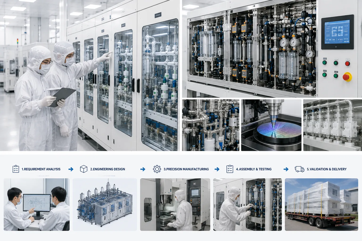
KOSEN SEMI delivers custom semiconductor equipment tailored to meet demanding fab specifications and overcome complex yield loss mechanisms. Backed by our advanced Engineering Capability and dedicated equipment support team, we work alongside your process engineering group to customize chemical dosing, safety enclosures, and single-wafer or batch wet process solutions.
Frequently Asked Technical Questions
Expert guidance on addressing critical wet process challenges, surface contamination issues, and international fab safety compliance.
How do you eliminate drying artifacts and water marks during wafer cleaning?
Water mark formation occurs when residual DI water droplets evaporate on hydrophobic silicon surfaces, leaving concentrated silica deposits or metallic contaminants. KOSEN SEMI wet process solutions and specialized wafer cleaning systems prevent drying defects by integrating Isopropyl Alcohol (IPA) vapor drying technology operating on the Marangoni principle. As the wafer is slowly lifted from the bath, surface tension gradients efficiently draw liquid away from the surface without leaving micro-droplets behind.
To protect fine pattern features, systems are reinforced with ultra-high purity heated Nitrogen (N2) knife purge mechanisms and variable speed lift controls. This ensures complete liquid displacement across high-aspect-ratio trench structures without causing pattern collapse.
What chemical filtration standards support particle control in 200 nm standard and optimized 100 nm processes?
Particle control is critical for preserving target yield in advanced node fabrication. KOSEN SEMI designs custom semiconductor equipment with continuous, high-flow chemical recirculation loops equipped with point-of-use PTFE and PFA membrane filters rated down to 20 nanometers or finer.
Our equipment support design minimizes dead legs and stagnant zones where particles typically aggregate. Paired with inline chemical concentration monitoring and auto-dosing capabilities, our wet processing systems maintain strict bath chemical purity and prolong bath lifecycle stability.
How do KOSEN SEMI wet benches comply with cleanroom safety and SEMI standards?
Operational safety and comprehensive equipment support are fundamental requirements in modern cleanroom chemical processing. All KOSEN SEMI wet benches are engineered in strict accordance with SEMI S2 (environmental, health, and safety) and SEMI S8 (ergonomics) global industry guidelines.
Enclosures utilize FM4910-certified fire-retardant materials such as PVC-C, PFA, and PVDF. Safety systems feature integrated CO2 or water-mist fire suppression, secondary containment piping for hazardous chemistries, optical leak detection sensors, and dedicated acid/alkali exhaust extraction hoods to safeguard both cleanroom operators and facility infrastructure.