Are you struggling to balance defect control, chemical compatibility, and high wafer throughput in your fab? Selecting the right semiconductor wet processing configuration is one of the most critical decisions you will make for overall yield performance and tool ROI.
Whether you are evaluating high-capacity batch immersion against ultra-clean single-wafer tools, or verifying fluoropolymer compatibility for aggressive etch chemistries, making the right choice requires deep technical insight. In this actionable guide to wet processing semiconductor equipment, you will learn how to evaluate tool architectures, prevent pattern collapse, and select the ideal solution for your production requirements.
Let's dive right in.
Core Chemistries and Reaction Dynamics in Semiconductor Wet Processing
RCA Cleaning Chemistry (SC1 / SC2) for Defect Removal
How do you remove stubborn particulate and ionic impurities simultaneously? The industry-standard RCA cleaning sequence relies on a targeted, two-step chemical dynamic:
-
- Standard Clean 1 (SC1: NH4OH / H2O2 / H2O): Operates at 70°C–80°C to strip organic residues and oxidize particles. SC1 continuously forms and dissolves a thin surface oxide layer, physically lifting sub-micron particles from the surface.
- Standard Clean 2 (SC2: HCl / H2O2 / H2O): Operates at 75°C–80°C to target trace alkali ions and metallic contaminants. SC2 converts insoluble metals into soluble complex chlorides, preventing chemical re-adsorption.
Acid Etching and Stripping: Piranha Etch (SPM) and Dilute HF
What is the safest protocol for heavy organic removal and target layer etching? We utilize specialized acid baths tailored to specific surface dynamics:
| Chemistry | Composition & Temp | Primary Function | Reaction Dynamic |
|---|---|---|---|
| Piranha Etch (SPM) | H2SO4 / H2O2 (120°C–150°C) | Photoresist stripping & organic removal | Dehydrates and oxidizes organic residues into soluble carbon dioxide and water. |
| Dilute HF (DHF) | HF / H2O (1:50 to 1:500, Ambient) | Native oxide stripping & substrate surface passivation | Selectively etches SiO2 while terminating silicon surfaces with hydrogen to prevent immediate re-oxidation. |
Alkaline and Solvent Processing for Anisotropic Etching and Lift-Off
How do you maintain structural crispness on non-silicon or compound substrates?
-
- Alkaline Solutions (TMAH / KOH): Deliver anisotropic etching along specific silicon crystallographic planes, ideal for 3D structures and MEMS release.
- High-Purity Solvents (NMP / DMSO): Dissolve cross-linked photoresists during metal lift-off without damaging sensitive metal lines or underlying films.
Chemical Kinetics, Inline Dosing, and Bath Temperature Control
How do you prevent bath degradation and maintain consistent etch rates across high-volume production in wet processing semiconductor lines?
-
- Tight Temperature Precision: Closed-loop heat exchangers hold bath temperatures within ±0.1°C, ensuring repeatable chemical reaction rates.
- Automated Inline Dosing: Real-time spiking systems monitor chemical concentration and inject fresh reagents, counteracting peroxide decomposition in SPM and SC1 baths.
- Boundary Layer Management: Fluid agitation dynamics minimize the stagnant boundary layer on the wafer surface, guaranteeing uniform mass transport across every square millimeter.
Tool Architectures: Single-Wafer Spin Processing vs. Automated Batch Wet Benches
Automated Batch Immersion Wet Bench Mechanisms and Limits
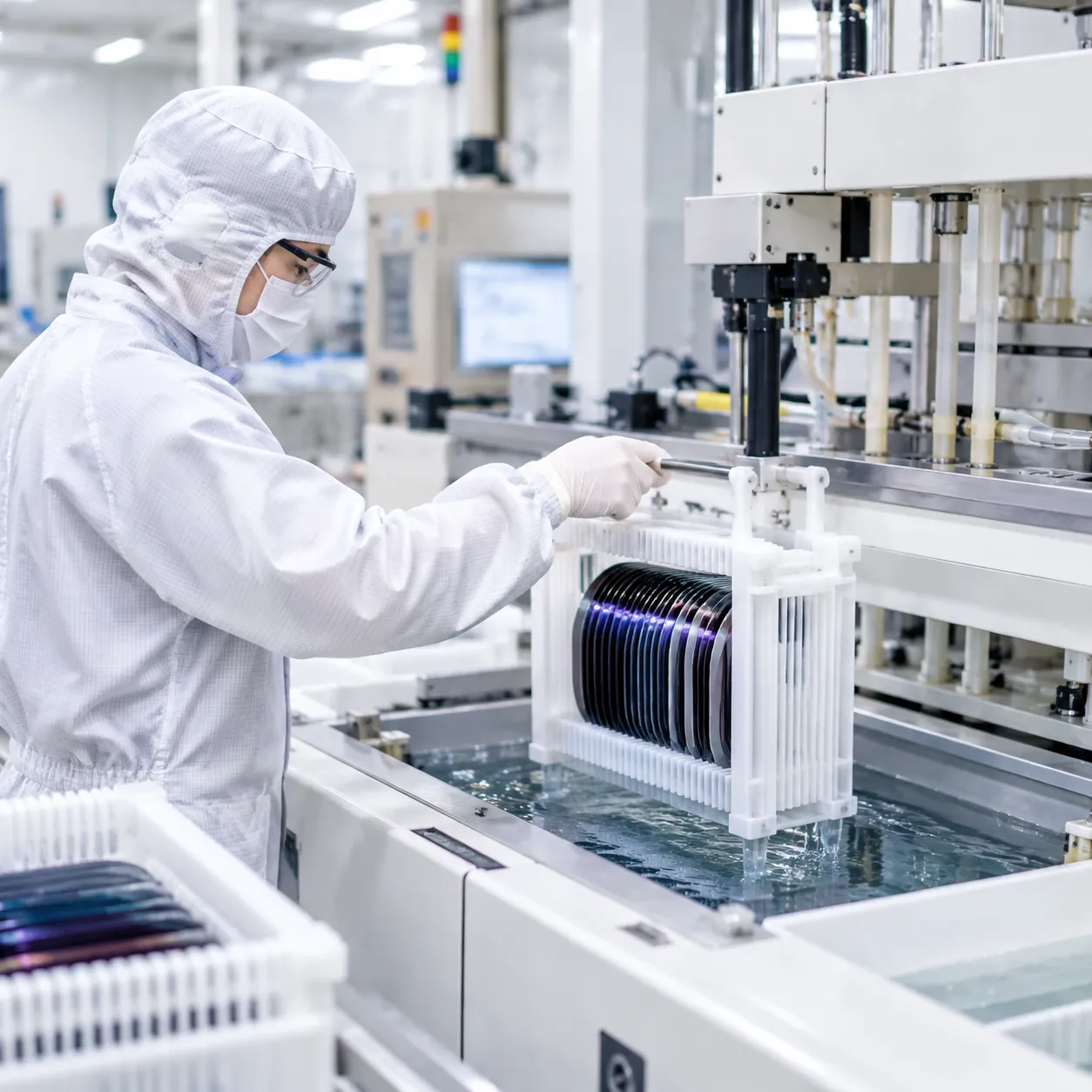
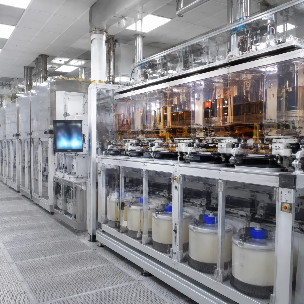
Batch immersion systems remain the backbone of high-volume manufacturing. By processing 25 to 50 wafers simultaneously in recirculated chemical baths, our automated semiconductor wet bench systems lower operational costs and maximize tool productivity.
-
- High-volume throughput: Processes hundreds of wafers per hour in a compact footprint.
- Bath recirculation: Integrated fluid dynamics maintain uniform bath temperatures and chemical concentrations.
- High-volume limits: Chemical drag-out between baths, fluid boundary layer limits, and particle re-deposition present distinct challenges for sub-10nm geometries.
Single-Wafer Spin Processing for Advanced Nodes and Compound Substrates
When manufacturing sub-10 nm features or high-value compound semiconductors like SiC and GaN, cross-contamination is unacceptable. Single-wafer spin processing dispenses fresh chemistry directly onto a rapidly spinning wafer surface, ensuring superior defect control and boundary layer renewal.
-
- Zero cross-contamination: Every wafer receives point-of-use, fresh chemical dispense.
- Enhanced boundary layer control: High rotational speeds and dynamic spray nozzles remove boundary layer resistance faster.
- Substrate flexibility: Ideal for warped, thin, or sensitive compound semiconductor wafers where bath immersion poses handling risks.
Comparative Selection Matrix for Semiconductor Wet Processing Tools
Review our detailed wet bench selection guide to evaluate tool configurations against your fab's yield goals.
| Feature | Automated Batch Wet Bench | Single-Wafer Spin Processor |
|---|---|---|
| Primary Focus | Maximum throughput & lowest cost of ownership | Extreme defect control & surface uniformity |
| Processing Capacity | 25–50 wafers per run | 1 wafer per chamber |
| Contamination Control | Moderate risk (recirculated chemical baths) | Zero risk (fresh chemical delivery) |
| Chemical Consumption | Low (extended bath re-use) | Higher (single-use dispense) |
| Ideal Substrates | Standard Si, legacy nodes, FEOL bulk cleans | Advanced Si nodes, SiC, GaN, thin wafers |
| Pattern Collapse Prevention | Standard drying methods | Direct integrated IPA Marangoni spin control |
Advanced Defect Control and Particle Removal in Semiconductor Wet Processing
How do you eliminate sub-100 nm nano-particles without damaging delicate structures or suffering pattern collapse? In high-density wet processing semiconductor lines, micro-contamination is a constant threat to yield. We combat this by pairing acoustic force and fine-pore chemical filtration with surface-tension-driven drying.
Megasonic Particle Agitation for Sub-100 nm Defect Control
Removing nano-sized particles from dense wafer features requires controlled physical energy. Standard acoustic cleaning can easily snap fragile gate lines if cavitation energy spikes.
-
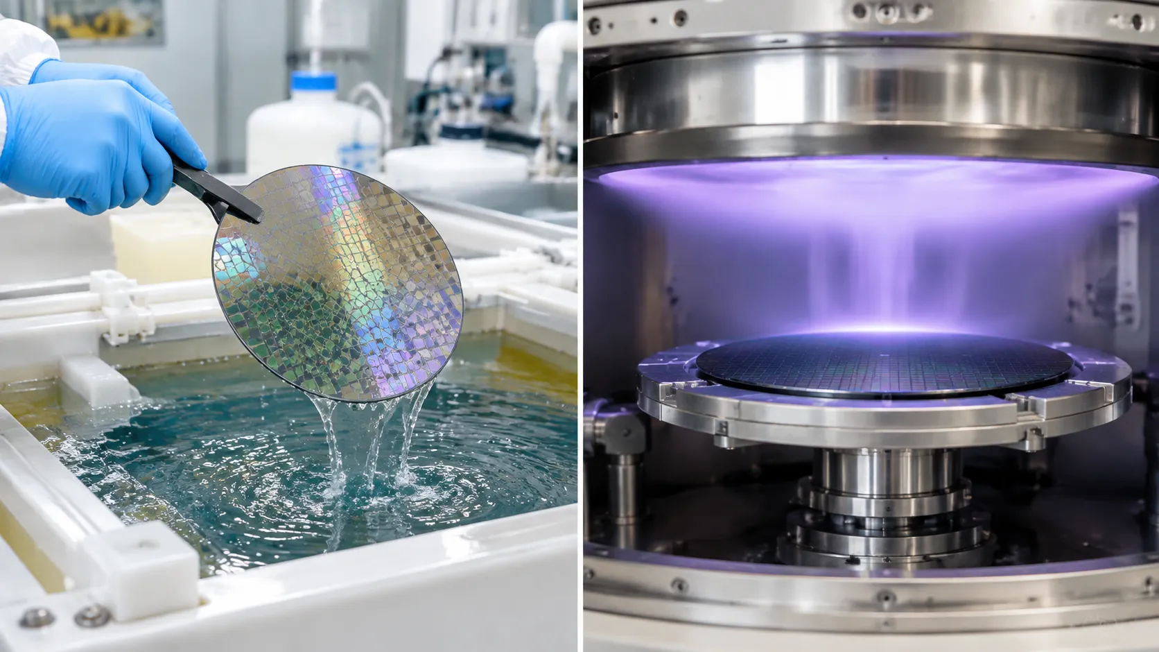
- Controlled Acoustic Micro-Streaming: We utilize multi-frequency megasonic transducers operating between 1 MHz and 3 MHz. This setup generates localized acoustic micro-streaming that overcomes the van der Waals forces binding sub-100 nm contaminants to the surface.
- Substrate Surface Safety: By tuning power density and sweeping frequencies, we strip physical defects without causing structural damage to sensitive 3D features.
Point-of-Use Chemical Filtration Down to 0.005 μm
Chemical bath purity directly impacts surface defect counts. Recirculated chemicals continuously accumulate micro-particles unless intercepted right before liquid delivery.
-
- Ultra-Fine POU Filtering: We integrate point-of-use chemical filtration units down to 0.005 μm (5 nm) directly into chemical supply lines.
- Active Contamination Control: Continuous inline recirculation through fluoropolymer membrane filters traps micro-particulates and trace gel defects before they ever reach the wafer surface.
- Integrated Delivery: This filtration setup comes fully integrated across our automatic wet bench systems, maintaining pristine bath chemistry throughout high-volume production runs.
IPA Marangoni Drying and Vapor Control to Prevent Pattern Collapse
As feature aspect ratios exceed 10:1, surface tension from conventional spin-drying pulls high-aspect structures together, leading to pattern collapse.
-
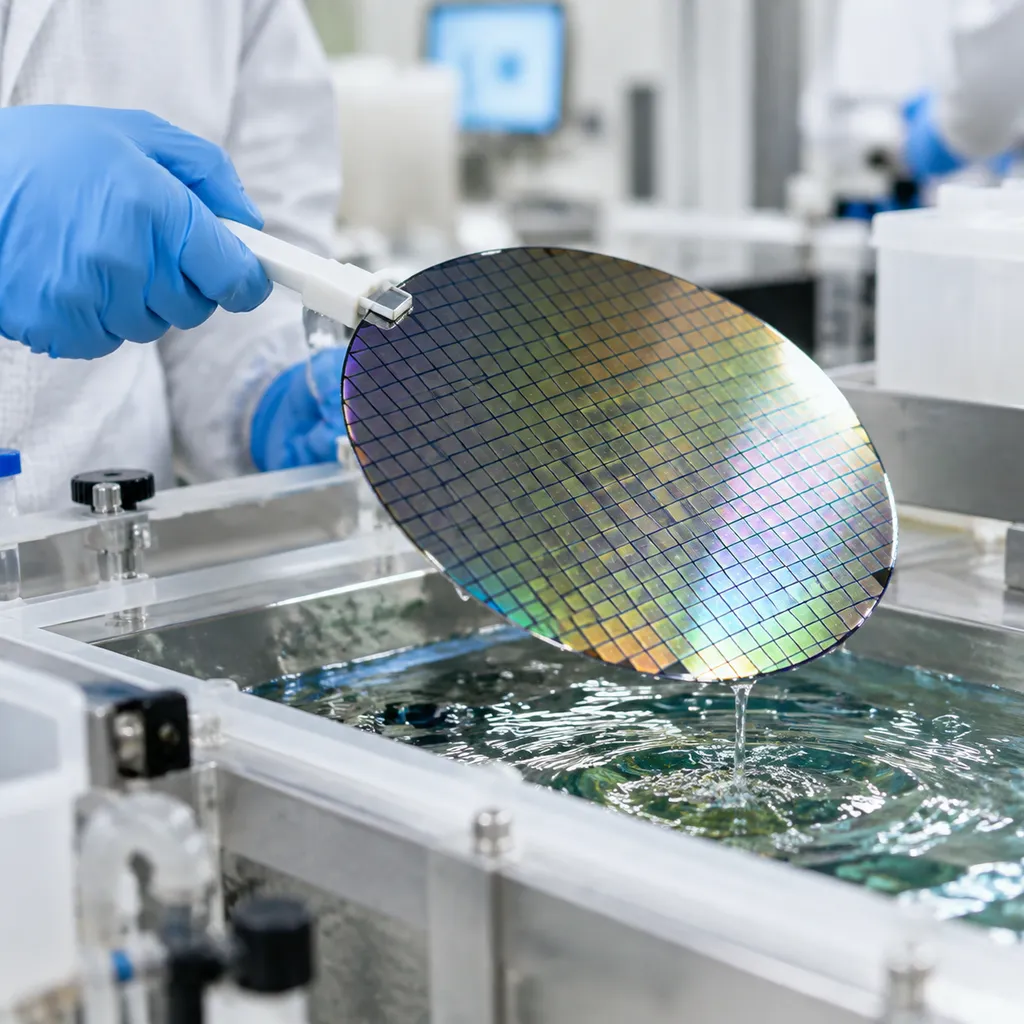
- Surface Tension Gradient: We employ isopropyl alcohol (IPA) Marangoni drying. By introducing a controlled IPA-N2 vapor gradient at the meniscus between deionized water and the lifting wafer, fluid surface tension drops close to zero.
- Zero Water-Mark Defect: Fluids roll off smoothly without pulling on delicate lines, delivering clean drying with zero water-mark defects.
- Vapor Concentration Control: Closed-loop N2/IPA vapor dosing ensures tight process control, preventing micro-condensation and keeping volatile organic emissions minimal.
| Defect Control Technique | Core Mechanism | Target Defect Size | Key Benefit |
|---|---|---|---|
| Megasonic Agitation | Acoustic micro-streaming (1–3 MHz) | Sub-100 nm particles | High particle removal efficiency without line damage |
| POU Chemical Filtration | 0.005 μm fluoropolymer filtration | 5 nm+ micro-contaminants | Prevents chemical bath particle buildup |
| IPA Marangoni Drying | Surface tension differential | Water-marks & line bridging | Achieves pattern collapse prevention on high-aspect features |
Equipment Construction, Material Compatibility, and Fluidics Safety
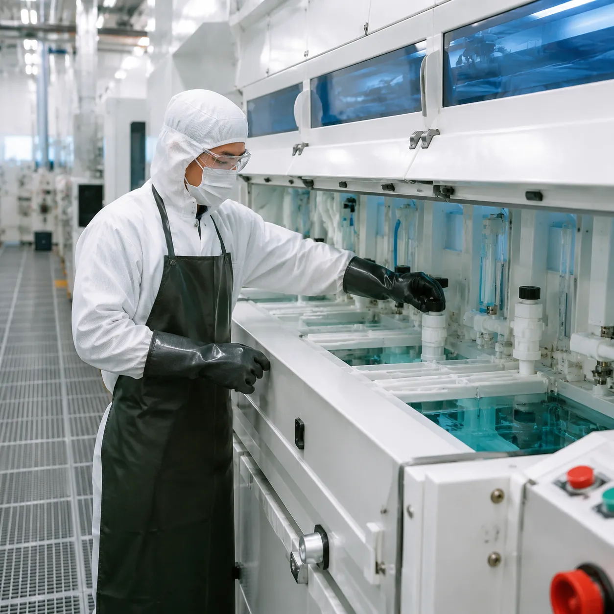
How do you guarantee sub-nanometer cleanroom purity while handling violent exothermic acid reactions? In semiconductor wet processing, tool durability and wafer yield depend entirely on structural material choices and fluid containment safety. We engineer every wet processing semiconductor platform with chemical-inert materials and redundant safety systems to protect both your wafers and your fab operators.
Wetted Material Selection: PFA, PTFE, PVDF, and Quartz
Will chemical leaching or thermal stress degrade your bath integrity during critical cleans? Fluoropolymer chemical bath containment and high-purity quartz are essential to prevent metal contamination and structural breakdown.
-
- High-Purity PFA: Used extensively in tubing, fittings, and valve bodies. High-purity PFA fluidics prevent trace metal leaching and withstand continuous exposure to hot, aggressive acids.
- PTFE (Teflon): Ideal for fully machined chemical baths, pump diaphragms, and seal surfaces requiring high thermal stability and universal chemical inertness up to 260°C.
- PVDF (Kynar): Applied in ambient chemical distribution lines, drainage networks, and structural support components where mechanical strength and cost-efficiency intersect.
- High-Purity Quartz: The primary material for high-temperature Piranha (SPM) baths and megasonic chemical processing due to its thermal shock resistance and ultra-low particle generation.
| Material | Max Working Temp | Primary Application | Key Benefit |
|---|---|---|---|
| PFA | 260°C | Chemical lines, manifolds, fittings | Zero ionic leaching, high flex life |
| PTFE | 260°C | Machined baths, valve seats | Universal chemical resistance |
| PVDF | 140°C | Ambient supply lines, outer sumps | High mechanical & tensile strength |
| Quartz | > 1000°C | Hot SPM baths, megasonic tanks | Superior purity under thermal stress |
SEMI S2/S8 Compliance and Enclosure Safety
How do you eliminate operator risk when handling gallons of concentrated hydrofluoric or sulfuric acid? We build all tool enclosures in strict accordance with SEMI S2 (environmental, health, and safety) and SEMI S8 (ergonomics) standards.
-
- FM4910-Certified Cabinetry: Constructed using fire-retardant polypropylene (FR-PP) shells to prevent ignition and stop flame propagation in cleanroom environments.
- Multi-Point Leak Detection: Optical and conductivity sensors placed throughout secondary containment sumps instantly trigger Emergency Off (EMO) fluid isolation.
- Exhaust Airflow Monitoring: Continuous differential pressure sensors ensure toxic acid vapors never escape the cabinet perimeter during operational cycles.
Advanced Fluid Distribution and Zero-Dead-Leg Architecture
Stagnant fluid pockets are silent killers of process repeatability, causing chemical decay, particle entrapment, and bacterial growth. We implement dual-containment piping and continuous-recirculation loops to guarantee point-of-dispense purity. Seamless equipment integration pairs these fluid systems directly with central chemical delivery units for automated, leak-free supply control.
-
- Dual-Containment Piping: Outer protective sleeve containment prevents pressurized chemical spray-outs in the event of a primary line rupture.
- Zero-Dead-Leg Valves: Compact diaphragm valve blocks eliminate static fluid traps, ensuring rapid chemical displacement and precise dose repeatability.
Fab Automation, Environmental Control, and Exhaust Abatement
Are chemical vapors, manual wafer handling risks, and soaring raw material costs bottlenecking your fab efficiency? Modern semiconductor wet processing requires total equipment autonomy, ultra-clean chemical delivery, and robust site safety. We build our wet processing equipment to seamlessly integrate with automated fab lines while neutralizing hazardous outputs directly at the tool level.
Robotic Wafer Handling and SECS/GEM Fab Automation Interface
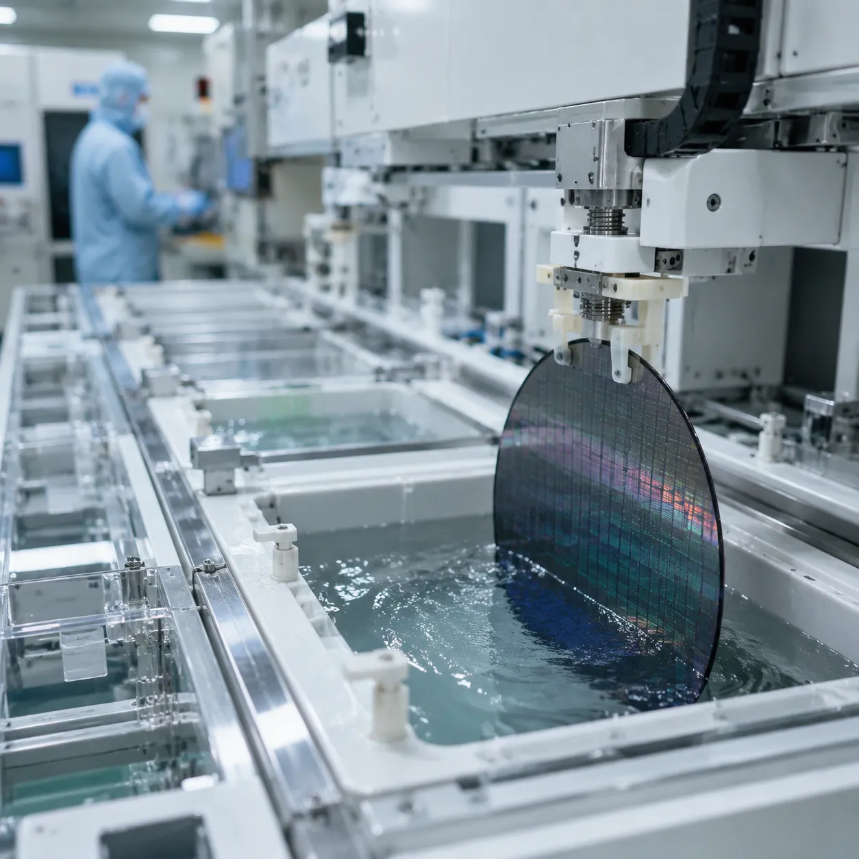
Eliminating human intervention inside the cleanroom drastically drops defect rates. Our automated wet bench platforms utilize high-precision robotic grippers and multi-axis transfer arms designed specifically for aggressive chemical environments.
-
- Full SECS/GEM Integration: Standardized E30/E37 protocols communicate directly with your MES for remote recipe selection, tracking, and process logging.
- Predictive Diagnostics: Real-time feedback continuously reports bath temperatures, fluid flow rates, and filter pressure drops.
- Gentle Transport Dynamics: Smooth acceleration profiles prevent fluid splash, micro-bubbles, and physical substrate shock during high-throughput runs.
By linking advanced chemical process management technology into factory automation networks, we give your team complete control over yields without stepping foot inside the process chamber.
Point-of-Use Exhaust Abatement Scrubbers for Toxic Acid Gas
Vaporized HF, HCl, and thermal nitric acid fumes pose severe risks to operator safety and facility ductwork. Treating toxic gas at the source prevents duct corrosion and optimizes fab emissions compliance.
An integrated chemical exhaust scrubber neutralizes volatile acid vapors right at the exhaust plenum of the wet tool.
| Parameter | Performance Spec |
|---|---|
| Abatement Efficiency | > 99.9% acid gas neutralization |
| Scrubber Mechanism | Multi-stage counter-current wet packed bed |
| Dosing Control | Closed-loop automated pH and liquid level monitoring |
| Construction | Flame-retardant PP / PVDF for total acid resistance |
Closed-Loop Chemical Recycling and Hazardous Effluent Reduction
Constantly dumping spent bath chemistries drives up procurement costs and stresses waste treatment facilities. Our wet processing semiconductor platforms incorporate closed-loop recycling loops to reclaim and reuse expensive process chemistries.
-
- Continuous Point-of-Use Filtration: Recirculation pumps push reagents through sub-micron filters to capture suspended particles during active bath cycles.
- Chemical Re-dosing: Automated inline chemical analyzers test bath concentration and inject fresh spikes, extending chemical lifetime by up to 300%.
- Effluent Segregation: Dedicated drain manifolds keep hazardous acid streams separate from solvent waste, simplifying downstream neutralization and lowering disposal fees.
Industrial Applications Across Mainstream and Compound Semiconductor Sectors
How do you maintain high yield when transitioning from planar silicon to complex 3D chiplets and hard wide-bandgap substrates? Every device architecture demands exact chemical parameters and precise physical delivery during semiconductor wet processing to eliminate defect sources without damaging sensitive features.
FEOL Gate Prep and BEOL Metal Cleaning
Integrated circuit manufacturing relies on precise contamination control at both early substrate prep and final metallization steps:
-
- Front-End-of-Line (FEOL): Ultra-clean gate oxide prep requires complete removal of trace organic impurities, metallic defects, and native oxides using targeted RCA clean chemistries.
- Back-End-of-Line (BEOL): Post-CMP cleaning and photoresist residue stripping require high chemical selectivity to clean trace polymers without etching exposed copper or aluminum interconnects.
Compound Semiconductor Wet Etching for SiC and GaN
Silicon carbide and gallium nitride substrates introduce tough chemical resistance challenges for power electronics fabrication:
| Substrate Material | Primary Wet Process | Key Processing Objective |
|---|---|---|
| Silicon Carbide (SiC) | Surface damage removal & defect etching | Removes mechanical lapping damage and exposes dislocations prior to epi-growth |
| Gallium Nitride (GaN) | Anisotropic wet etching & substrate prep | Controls mesa side-wall profiles while ensuring surface passivation |
Using specialized wet processing semiconductor equipment guarantees consistent bath temperatures and etch uniformity across these robust compound materials.
Advanced Packaging Wet Processing: TSV Cleaning and Micro-Bumping
Modern 2.5D/3D packaging structures rely on thorough fluid penetration into high-aspect-ratio features. In high-density advanced semiconductor packaging applications, wet processing cleans deep Through-Silicon Vias (TSVs), strips thick photoresists, and removes flux residue after micro-bumping. Uniform fluid delivery prevents voiding and ensures clean surface contact for wafer bonding.
MEMS and Optoelectronics Sacrificial Layer Release Etching
Micro-sensors and photonic devices require precise wet etching to free moving structural elements:
-
- Sacrificial Layer Removal: Controlled HF-based wet chemical etching selectively dissolves silicon dioxide layers to release micro-machined beams and membranes.
- Anti-Stiction Rinsing: Chemical rinsing protocols minimize surface tension during drying, preventing delicate suspended micro-structures from collapsing or sticking together.
Custom Semiconductor Wet Processing Solutions and KOSEN SEMI Advantage
Standard tool designs often fall short when you need precise chemistry control within unique cleanroom footprints. We engineer tailored systems directly around your target process windows to deliver high-yield semiconductor wet processing setups without forcing standard off-the-shelf compromises.
CAD-Driven Engineering and Rapid Prototyping
We use advanced 3D modeling and fluidics simulations to design high-efficiency architectures built specifically for your process chemistries:
-
- 3D Spatial Optimization: Custom frame dimensions and bath layouts designed to maximize tool footprint efficiency in tight fab bays.
- Rapid Prototyping: Fast turnarounds on specialized bath geometries, fluid manifolds, and specialized single-wafer processing chucks.
- Tailored Application Support: Purpose-built custom semiconductor equipment optimized for specialized cleaning, etching, and surface passivation workflows.
ISO Class 5–7 Cleanroom Assembly Standards
Defect control begins long before the tool reaches your floor. We build every wet processing semiconductor system under strict environmental protocols to eliminate contamination risks before final delivery:
-
- Controlled Assembly: Tool fabrication, fluidic integration, and pre-commissioning conducted entirely inside ISO Class 5–7 cleanrooms.
- High-Purity Fluidics: Ultra-pure orbital welding and high-purity PFA fluidic piping prevent metallic leaching and micro-particle contamination during chemical chemical processing.
Global Track Record Across HVM Fabs and R&D Facilities
Whether you are scaling high-volume production or running flexible R&D experiments, our equipment adapts seamlessly to your operational scale:
-
- High-Volume Fabs: Built for 24/7 continuous duty cycles, automated chemical bath dosing, and full SECS/GEM fab automation interface integration.
- R&D Cleanrooms: Modular, customizable wet benches engineered for rapid chemistry changeouts and multi-substrate research.
- Proven Reliability: Backed by a strong global presence and a proven wet bench installation track record across leading semiconductor manufacturing hubs.
Frequently Asked Questions About Semiconductor Wet Processing
Single-Wafer Spin Processing vs. Automated Batch Wet Benches
We help fabs evaluate tool architectures based on node requirements, footprint, and wafer throughput. Both technologies serve critical roles in modern semiconductor wet processing:
| Feature | Single-Wafer Spin Processing | Automated Batch Wet Benches |
|---|---|---|
| Primary Application | Advanced nodes (<7 nm), compound semiconductors | High-volume manufacturing (HVM) legacy nodes |
| Wafer Throughput | Lower per chamber (expanded via multi-chamber tools) | 25 to 50 wafers per batch lot |
| Cross-Contamination Risk | Near-zero (fresh chemistry dispensed per wafer) | Low (managed via continuous filtration & overflow) |
| Chemical Consumption | Higher dispense rate per single wafer | Lower cost per wafer via recirculating baths |
For tight defect budgets on leading-edge processes, single-wafer cleaning systems deliver precise surface control. For maximum wafer output per hour on standard logic and memory, high-capacity batch wafer cleaning systems offer superior cost efficiency.
How RCA Clean Removes Organic and Metallic Contaminants
The standard RCA clean relies on a two-step chemistry sequence to achieve pristine silicon wafer surfaces:
-
- Standard Clean 1 (SC-1): Combines ammonium hydroxide, hydrogen peroxide, and water (NH4OH / H2O2 / H2O) at elevated temperatures (70°C–80°C). It oxidizes organic residues and strips sub-micron particles through controlled micro-etching of the silicon surface.
- Standard Clean 2 (SC-2): Follows with a mixture of hydrochloric acid, hydrogen peroxide, and water (HCl / H2O2 / H2O) at 70°C–80°C. It dissolves alkali cations and trace metallic impurities, forming soluble complexes that prevent metal ion re-adsorption.
Fluoropolymer Selection for High-Purity Wet Chemical Delivery
Building a reliable wet processing semiconductor delivery system requires matching specific fluoropolymers to chemical aggressiveness and temperature profiles:
-
- High-Purity PFA: Our standard choice for chemical tubing, fittings, and zero-dead-leg valve bodies due to its smooth surface finish, high flexibility, and exceptionally low metallic extractables.
- PTFE: Ideal for machined chemical bath liners, pump diaphragms, and hot acid immersion tanks exposed to extreme temperatures.
- PVDF: Used for rigid secondary containment piping, structural manifold supports, and ambient drain lines requiring high mechanical strength.
SECS/GEM Interface Integration for Automated Fabs
SECS/GEM protocols establish standard communication between wet processing equipment and the fab's central Manufacturing Execution System (MES). This integration automates critical operational controls:
-
- Recipe Management: Automatically downloads verified bath immersion times, chemical dispense sequences, and dry profiles based on incoming lot IDs.
- Inline Sensor Tracking: Transmits real-time feedback on bath temperatures, chemical dosing concentrations, flow rates, and filter pressure differentials.
- Interlock & Safety Monitoring: Provides instant automated alerts, isolating chemical delivery and triggering point-of-use exhaust scrubbers the moment a leak or hardware fault is detected.