Formula details
Product Details
Overview
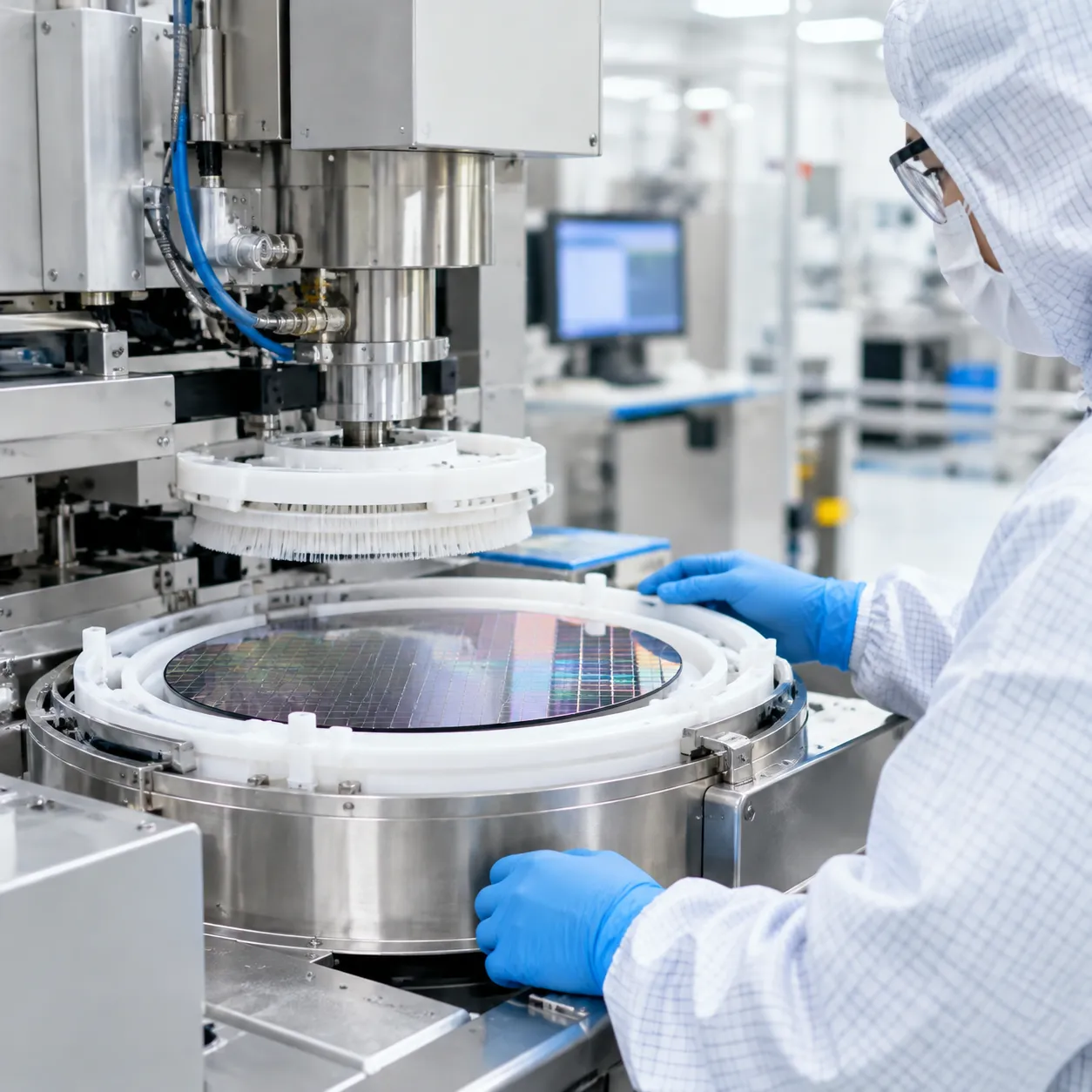
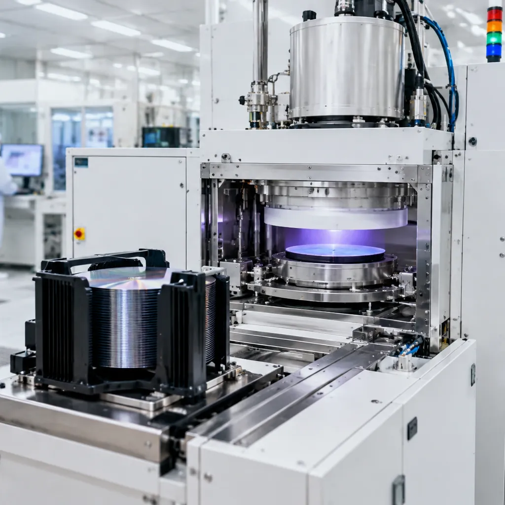
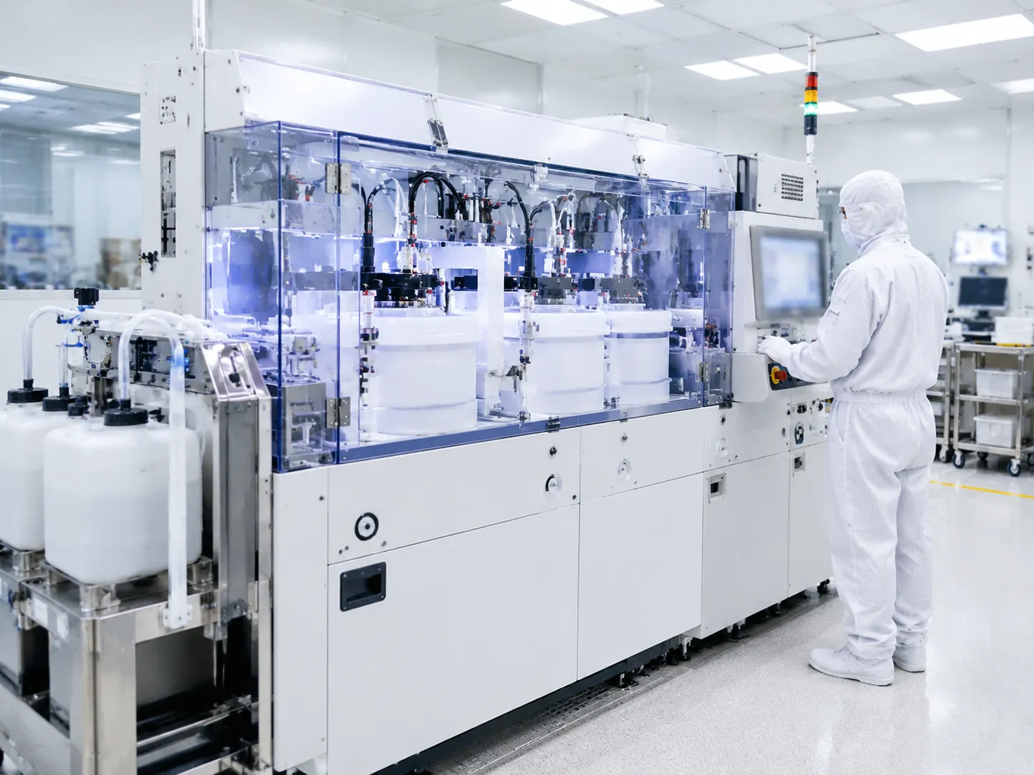
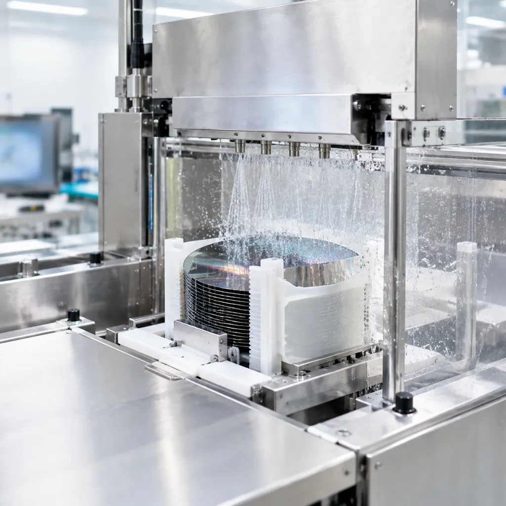
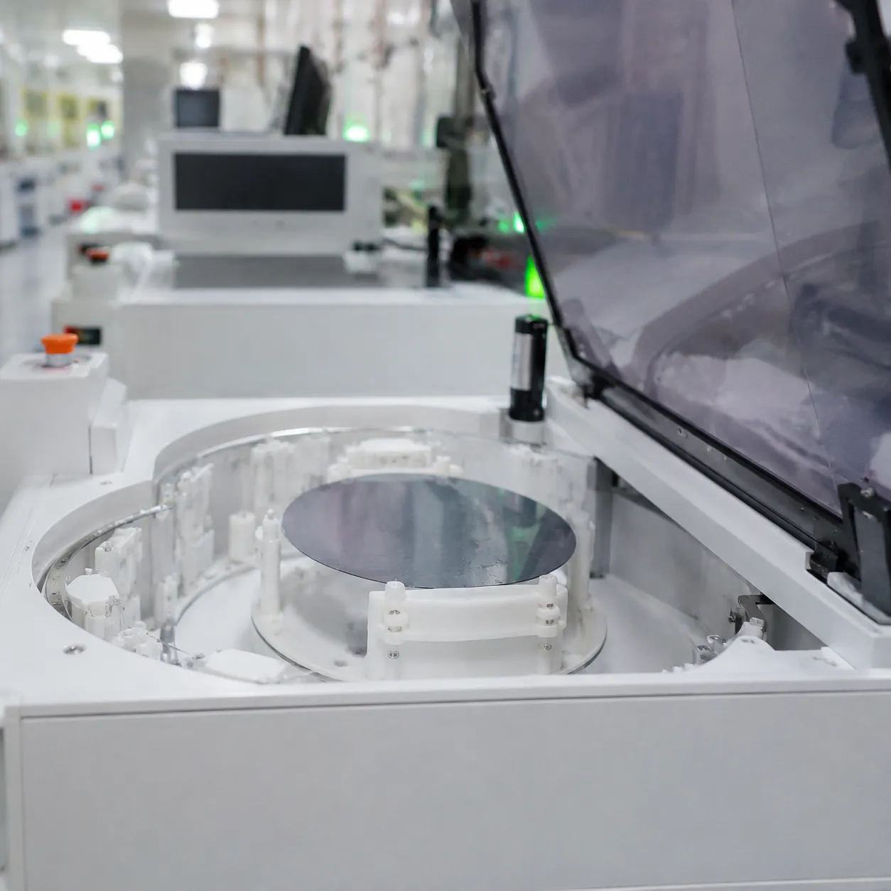
Single Wafer Wet Processing Equipment Overview
The Single-Wafer Advantage
Batch processing introduces chemical carryover and bath degradation over time. Our single wafer spin processor platform isolates each substrate to maintain strict defectivity control:
-
- Eliminates Particle Redeposition: Continuous dynamic fluid flow ensures dislodged particles wash directly to drain without reattaching to the wafer surface.
- Prevents Chemical Carryover: Independent chemical dispense arms isolate process steps, removing chemical drag-out between active chemical and rinse steps.
- Consistent Bath Integrity: Fresh, point-of-use chemical dosing eliminates bath aging, concentration drift, and bath degradation.
Core Processing Mechanics
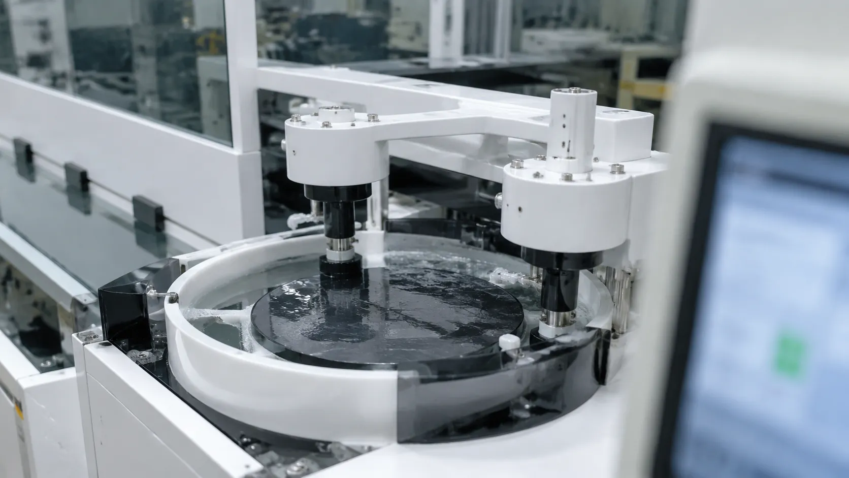
Our wafer surface treatment system integrates precise physical and fluidic mechanics into a compact process chamber:
| Processing Feature | Operational Mechanism | Yield Benefit |
|---|---|---|
| Controlled Spin-State | Dynamic rotation (1–6,000 RPM) with closed-loop acceleration control | Maintains uniform liquid boundary layer thickness across 150mm to 300mm wafers |
| Micro-Porous Chemical Spray Tool | High-dispersion, uniform mist nozzles | Maximizes surface wetting while reducing active chemical volume consumption |
| Megasonic Wafer Cleaning Tool | High-frequency megasonic transducer integration | Removes sub-micron particles without damaging delicate pattern structures |
Chemical Recirculation & Footprint Efficiency
We optimize cost-of-ownership (CoO) through intelligent fluidics and compact platform design:
-
- Point-of-Use Micro-Filtration: Continuous inline chemical recirculation utilizes high-efficiency filters targeting particles down to 0.005 μm, maintaining chemical purity across extended production runs.
- 30% Footprint Reduction: Streamlined chamber architecture and consolidated cabinet fluidics save valuable cleanroom floor space while boosting yield per square meter.
Core Process Applications and Compatible Substrates
Target Substrate Materials
Our single wafer cleaning equipment safely handles standard, hard, and ultra-thin substrates without physical stress or edge damage:
-
- Silicon (Si): Full support for 150mm, 200mm, and 300mm prime, reconditioned, and patterned wafers.
- Silicon Carbide (SiC): Robust fluidics designed for aggressive chemistries required in wide-bandgap substrate processing.
- Gallium Nitride (GaN): Precise chemical dosing for epitaxial layer surface preparation and cleaning.
- Thin & Bonded Wafers: Contactless non-contact edge-grip mechanisms for safe handling down to thin-wafer thresholds.
FEOL & BEOL Wet Processing Applications
Our single wafer wet etch equipment targets critical yield-limiting steps across Front-End-of-Line (FEOL) and Back-End-of-Line (BEOL) operations:
-
- FEOL Critical Surface Cleaning: Precise native oxide etching using diluted HF (DHF), pre-gate oxide cleaning, and particle removal via standard SC1/SC2 chemistries.
- BEOL Etching & Cleans: Controlled metal film etching, selective layer stripping, and post-CMP residue cleaning with zero cross-contamination.
| Process Category | Target Application | Key Process Advantage |
|---|---|---|
| FEOL | Native Oxide Etching & Surface Prep | Direct chemical injection prevents re-oxidation |
| BEOL | Selective Metal Etch & Post-CMP Clean | High selectivity with zero sub-surface damage |
| Packaging | Micro-Bump & TSV Cleaning | Deep-trench chemistry penetration with megasonics |
| MEMS | Sacrificial Layer Etch | Precise etch-stop control on delicate structures |
Advanced Packaging & Power Device Integration
High-density integration and compound semiconductors require specialized surface preparation and chemical delivery:
-
- Advanced Packaging & TSV: Deep Through-Silicon Via (TSV) wet processing, micro-bump cleaning, and heavy advanced packaging photoresist stripping equipment applications.
- Compound Semiconductor Prep: Surface treatment and defect-free preparation for SiC/GaN high-power electronics, leveraging our integrated semiconductor wet processing systems for 300mm wafers and smaller compound substrates.
- MEMS & Optoelectronics: Controlled surface modification, precise sacrificial layer release, and complete residue removal for sensitive micro-actuators and optical sensors using our flexible wafer surface treatment system.
Technical Specifications: Single Wafer Wet Processing Equipment
| Parameter | Specification |
|---|---|
| Supported Wafer Sizes | 150mm (6"), 200mm (8"), 300mm (12") |
| Tool Throughput | Up to 120 WPH (wafers per hour) |
| Particle Removal Efficiency (PRE) | >99% at ≥19nm particles |
| Chemical Compatibility | SPM, DHF, BOE, SC1, SC2, solvents |
| Fluid Pathway Materials | UHP PFA, PTFE, PVDF |
| Chemical Dosing Precision | ±0.05% |
| Rotation Speed Range | 1 – 6,000 RPM (programmable ramping) |
| Cleanroom Environment | ISO Class 5 to ISO Class 7 compatible |
| Safety Compliance | SEMI S2 / S8 certified, ISO 9001 compliant |
Precision Fluidics and Chemical Control
-
- Ultra-High Purity Fluidics: All fluid pathways utilize UHP PFA, PTFE, and PVDF components to eliminate ionic leachables and micro-contamination in advanced node processing.
- Dosing Precision: Closed-loop flow controllers maintain liquid dispensation accuracy within ±0.05%, drastically cutting raw chemical consumption across wet chemistry processing systems.
- Particle Removal Efficiency: Integrated megasonic agitation paired with micro-porous chemical spray arms delivers PRE rates exceeding 99% on challenging surface profiles without damaging delicate structures.
Operational Motion & Cleanroom Integration
-
- Dynamic Spin Control: High-torque brushless motors provide smooth speed transitions from 1 to 6,000 RPM, optimizing fluid boundary layers during chemical dispense and ensuring complete drying during high-speed spin steps.
- Fab & Safety Certification: Designed around strict SEMI S2 compliance and safety standards, our single wafer cleaning equipment incorporates localized exhaust enclosures, dual-containment piping, and automatic leak-detection interlocks.
System Architecture & High-Purity Engineering Features
We design our single wafer wet processing equipment to withstand aggressive chemical environments while maintaining ultra-clean fab standards. By combining anti-corrosive structural materials with ultra-high purity fluidics, our architecture maximizes yield and hardware uptime.
Anti-Corrosive Enclosure Architecture
Chemical durability starts at the structural frame. We build our tool cabinets using high-grade Polypropylene (PP), Polyvinyl Chloride (PVC), Polyvinylidene Fluoride (PVDF), and structural Perfluoroalkoxy (PFA) supports.
Corrosion Resistance: Eliminates chassis degradation from continuous exposure to hot concentrated acids, alkalis, and solvents.
Cleanroom Isolation: Isolates process chambers to maintain strict ISO Class 5 air quality inside the tool cabinet.
Advanced Chemical Delivery & Fluidics
Our chemical delivery circuits ensure exact dosing without chemical carryover or particle generation. Through advanced chemical process management, we maintain tight process control across every single-wafer cycle.
UHP Dual-Containment Piping: Protects against leaks using nested Ultra-High Purity (UHP) PFA and PTFE fluid pathways.
Precision Thermal Control: In-line heat exchangers maintain chemical bath temperatures within ±0.1°C for consistent etch rates.
Multi-Stage Exhaust Mitigation Integration
Safe chemical vapor extraction is critical for fab environmental standards. Our semiconductor wet processing equipment features direct-coupled exhaust mitigation designed for seamless integration with point-of-use acid gas scrubbers.
Targeted Fume Extraction: Multi-zone exhaust routing prevents vapor condensation inside the processing chamber.
Fab Safety Protocols: Differential pressure sensors automatically trigger safety interlocks if exhaust airflow drops below baseline limits.
| Architecture Feature | Material / Design Standard | Key Operational Advantage |
|---|---|---|
| Main Enclosure | Structural PP / PVDF / PFA | Complete immunity to acid and solvent corrosion |
| Fluid Pathways | UHP PFA / PTFE Dual-Containment | Zero metallic leaching and secondary leak protection |
| Thermal Modules | Closed-loop inline heating | Uniform chemical reaction kinetics and precise etch depth |
| Exhaust Integration | Direct scrubber coupling | Real-time fume containment and cleanroom air safety |
Smart Fab Automation & SECS/GEM Control Architecture
Robotic Substrate Handling
Fragile, ultra-thin, or warped substrates require specialized care to eliminate yield loss from mechanical stress during transfer.
Edge-Grip & Vacuum End-Effectors: High-precision non-contact vacuum chucks or non-edge-bead edge-grip robotic arms prevent physical contact with critical active surfaces.
Fragile Wafer Control: Custom acceleration and deceleration profiles prevent wafer micro-cracks during loading into high-spin chambers.
Substrate Alignment: Integrated optical sensors continuously verify wafer position, maintaining high positioning repeatability.
SECS/GEM Integration
As a fully SECS/GEM compliant wet processing system, our platform establishes continuous communication with your fab's master control systems.
Real-Time MES Tracking: Automated recipe downloading, lot tracking, and substrate pass/fail verification directly through your host MES.
Data Logging & Traceability: Real-time collection of rotation speeds, chemical flow rates, temperature profiles, and megasonic power outputs for every processed wafer.
Host Control: Full support for SECS-I, SECS-II, and GEM standard communications for automated factory dispatching and remote tool management.
Advanced PLC Control Architecture
We build our single wafer processing equipment with industrial PLC control systems that balance deep process flexibility with cleanroom operational security.
| Control Feature | Operational Capability |
|---|---|
| Recipe Storage | Stores >500 multi-step custom recipes with flexible dynamic fluid and timing controls |
| User Interface | High-resolution touchscreen GUI displaying real-time fluidic animations and sensor telemetry |
| Access Control | Multi-level passcode security (Operator, Process Engineer, Maintenance, Administrator) |
| Closed-Loop Feedback | Continuous sensor monitoring for high-yield performance in automated wafer cleaning systems |
Safety Interlocks, Environmental Protection & Quality Standards
We build our single wafer wet processing equipment with fully redundant safety interlocks and smart chemical recovery to ensure absolute operator safety and high-yield cleanroom performance.
| Safety & Quality Module | Technical Mechanism | Fab & Environmental Impact |
|---|---|---|
| Fluid Leak Protection | Multi-point optical leak sensors with auto-shutoff | Instant chemical isolation under 50ms to prevent room contamination |
| Thermal Interlocks | SEMI S2 certified over-temperature hardware cutoffs | Eliminates fire hazards and protects chemical distribution lines |
| Chemical Recirculation | Integrated closed recycle loops with inline filtration | Reduces chemical waste and lowers fab effluent processing costs |
| Quality Management | ISO 9001 compliant manufacturing workflows | Guarantees hardware reliability and long-term yield consistency |
Built-in Operator Safety & SEMI S2 Compliance
Hazardous chemical handling requires constant monitoring. Our single wafer cleaning equipment incorporates optical leak detection sensors placed across all low-point drainage pans, valve manifolds, and pump cabinets. If a line ruptures, the system automatically isolates chemical supply valves and halts fluid flow instantly. SEMI S2 thermal interlocks continually monitor chemical baths and inline heaters, cutting power automatically if operating temperatures exceed configured safety thresholds.
Chemical Recovery & Yield Assurance
To lower cost-of-ownership (CoO) and meet strict environmental mandates, our single wafer wet processing equipment uses active chemical recycle loops. These loops filter and re-route expensive process chemicals back into the delivery stream, extending chemical lifespan while maintaining low defect levels. Every tool we produce aligns with ISO 9001 quality standards to ensure long-term tool uptime and defect-free wafer processing across every shift.
Custom Engineering & Global Service Infrastructure
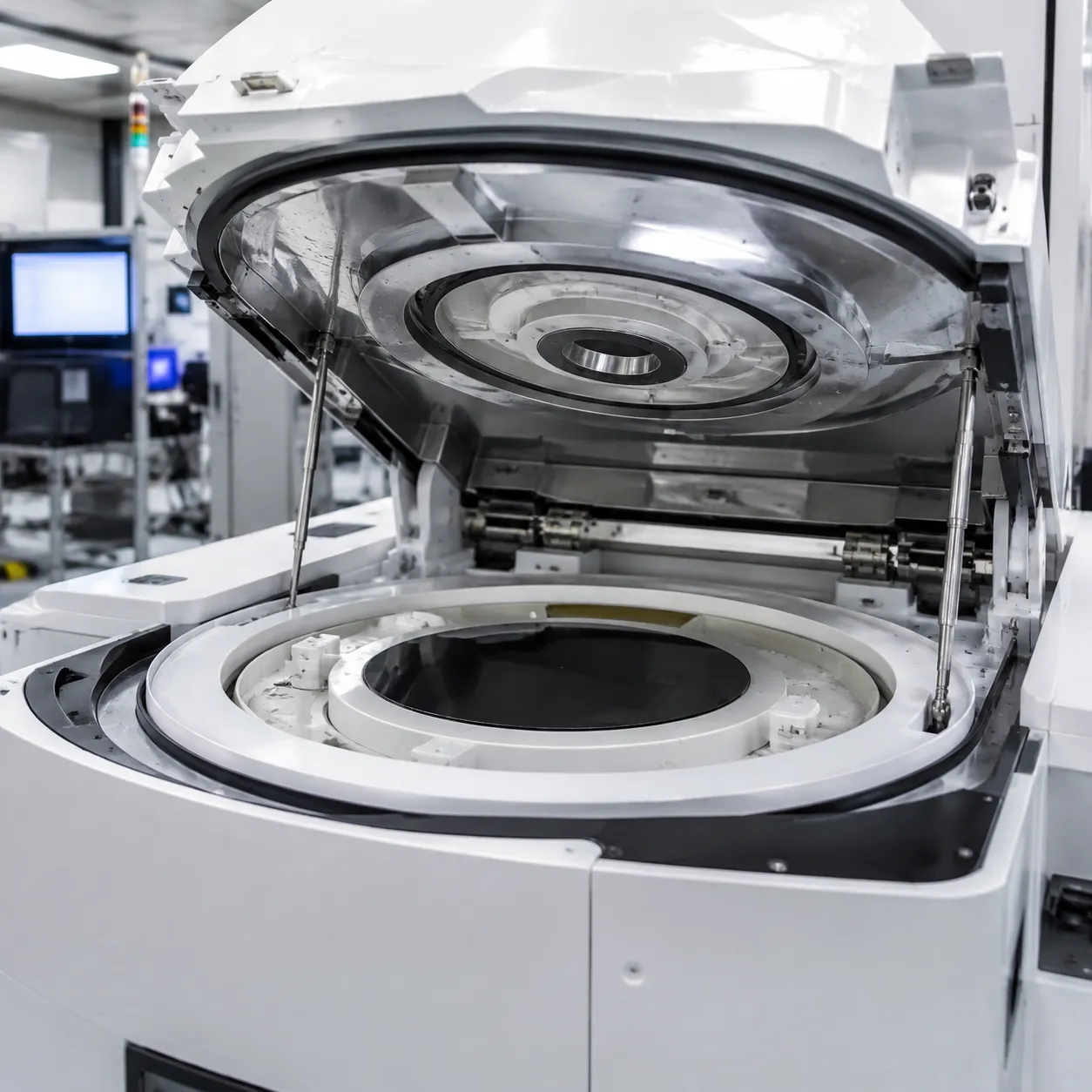
We build our single wafer wet processing equipment around modular hardware architectures, allowing us to adapt chamber layouts, dispense manifolds, and chemical delivery systems to your exact cleanroom footprint. Leveraged by our advanced engineering capabilities, we deliver fast-turnaround OEM and ODM design modifications in under 4 weeks to keep your expansion schedules on track.
Scalable Deployment Across Fab Environments
Our single wafer cleaning equipment scales seamlessly across every stage of device manufacturing:
-
- R&D & Pilot Lines: Compact, flexible single-chamber tools configured for quick recipe changes and process qualification.
- Commercial Fabs: High-throughput multi-chamber platforms designed for continuous 24/7 operation and maximum WPH efficiency.
- Specialized Tool Integrations: Tailored chassis configurations built for custom wet process stations handling non-standard wafer shapes, fragile compound semiconductors, or ultra-thin substrates.
24/7 Global Support & Spare Parts Logistics
Unplanned downtime directly impacts wafer yield. We maintain a worldwide support ecosystem to ensure maximum uptime for all our semiconductor wet processing equipment installations:
-
- 24/7 Field Engineering: Dedicated technical support teams available around the clock for emergency response, system diagnostics, and hardware tuning.
- Rapid Spare Parts Fulfillment: Regional hub inventories stocked with high-wear UHP PFA/PTFE valves, nozzles, and sensors for overnight delivery.
- Lifecycle Optimization: Ongoing process calibration, routine safety interlock checks, and modular upgrades to extend tool operational lifetime.
Frequently Asked Questions
Eliminating Cross-Contamination vs. Batch Benches
Unlike traditional batch wafer cleaning systems where multiple substrates submerge in shared chemical baths, single wafer wet processing equipment treats each wafer individually with fresh, point-of-use chemical delivery. We isolate every substrate on a high-speed spin chuck and direct spent chemicals straight to exhaust drains, preventing particle redeposition, chemical carryover, and bath degradation.
Particle Removal Efficiency (PRE) with Megasonic Agitation
Our integrated megasonic cleaning technology delivers a Particle Removal Efficiency (PRE) exceeding 98% for nanoparticles down to 19 nm. By generating precise acoustic cavitation in the fluid layer, the system breaks boundary layer resistance and dislodges stubborn micro-particles without causing structural damage or pattern collapse on delicate substrates.
SECS/GEM Integration with Fab MES Architecture
Our single wafer cleaning systems feature native SECS/GEM (SEMI E30/E37) software compliance to establish immediate two-way communication with your fab's Manufacturing Execution System (MES). Key capabilities include:
-
- Automated Recipe Management: Syncs process steps, fluid temperatures, and spin profiles based on wafer lot IDs.
- Real-Time Sensor Tracking: Logs chemical flow rates, megasonic power output, and chamber pressure for 100% traceability.
- Instant Safety Interlocks: Halts processing automatically if telemetry deviates from your strict yield window.
Related Sources
- https://www.rena.com/en/news
- https://www.researchgate.net/publication/3942522_Single_wafer_cleaning_and_drying_Particle_removal_via_a
- https://www.rena.com/en/products/semiconductor/semiconductor-wet-solutions-for-lab-or-
- https://semiconductorx.com/
- https://jstmfg.com/product/single-wafer-wet-process-system/