Formula details
Product Details
Overview
Proprietary Wet Chemical Processing Architecture
| Subsystem | Engineering Specification & Function |
|---|---|
| Chemical Delivery & Filtration | POU sub-0.05 µm PTFE; closed-loop spiked |
| Thermal & Fluid Dynamics | ±0.5°C precision up to 180°C |
| Acoustic Cleaning / Agitation | 0.8–2.0 MHz multi-frequency megasonics |
| Substrate Transfer Automation | Dual-end-effector robot; dry-to-dry path |
Precision Chemical Delivery and Inline Filtration
Yield loss from micro-particles and chemical concentration drift stalls production lines. We eliminate these failure modes at the source:
-
- Point-of-Use (POU) Filtration: High-flow, all-fluoropolymer filter housings capture particles down to sub-0.05 µm, stripping out trace contaminants right before bath entry.
- Closed-Loop Dosing: Flow-meter-driven spiked replenishment compensates for evaporation and bath depletion in real time, locking in steady-state chemical concentration.
- PTFE/PFA Fluid Paths: 100% pure virgin fluoropolymer lines prevent ionic leaching, even when running aggressive chemistries like concentrated HF, BOE, and nitric acid mixes.
Thermal and Fluid Dynamics in High-Temperature Baths
High-temperature chemical processing requires aggressive thermal stabilization without creating localized hot spots or bubble stagnation.
-
- Indirect Infrared & Immersion Heating: Baths reach operating temperatures up to 180°C with ±0.5°C within-bath uniformity, critical for hot phosphoric acid nitride strips.
- Optimized Recirculation Weir Design: Continuous edge-overflow weirs remove surface particulates and bubbles instantly, maintaining stable boundary-layer laminar flow across every substrate.
- Vapor-Sealed Covers: Automated bath lids prevent ambient evaporative cooling and contain toxic vapors during idle and active etch cycles.
Multi-Frequency Megasonic Agitation
To clean and etch sub-micron, high-aspect-ratio patterns without pattern collapse, physical shear forces must be tightly managed:
-
- Tunable Acoustic Windows: Multi-frequency megasonics operate between 800 kHz and 2.0 MHz, generating micro-acoustic streaming without destructive cavitation.
- Pattern Damage Prevention: Eliminates structural damage on fragile, high-aspect-ratio fin structures and MEMS beams while clearing sub-surface residues and entrapped air pockets.
- Uniform Energy Distribution: Transducer arrays ensure planar acoustic field density across full 200 mm and 300 mm wafer diameters.
Robotic Wafer Handling and Contamination Interlocks
Cross-contamination between acid etching stations, chemical clean baths, and final rinse tanks ruins process integrity. Our dry-to-dry handling platform enforces complete physical separation:
-
- Dual-End-Effector Transfer Robots: Dedicated, chemically inert end-effectors isolate wet acid-exposed wafers from dry incoming and outgoing FOUP cassettes.
- Anti-Cross-Contamination Drip Trays: Dynamic catch trays deploy under robot arms during transit to stop chemical carryover above adjacent processing tanks.
- Physical Hardware Interlocks: Real-time optical sensors detect carrier position, cassette engagement, and liquid level status to halt transfer sequences before any mechanical or chemical collision occurs.
Comprehensive Chemical Etch and Surface Preparation Recipes
Our wet etch tool semiconductor platforms support high-selectivity chemical etching and robust multi-step surface preparation across standard silicon and wide-bandgap substrates.
Selective Dielectric and Oxide Etching with BOE and Hot Phosphoric Acid
Dielectric layers require high etch selectivity without attacking underlying substrate materials:
- Silicon Nitride Stripping: Dedicated quartz vessels running hot phosphoric acid (H₃PO₄) at operating temperatures from 150°C to 180°C. Integrated closed-loop spiked chemical replenishment and boiling-point monitoring maintain constant water-to-acid ratios, guaranteeing repeatable nitride-to-oxide selectivity (>50:1).
- Controlled Oxide Removal: Precision buffered oxide etch (BOE / BHF) baths deliver stable, linear etch rates for thermal oxides, TEOS, and PSG films while preventing sub-surface pinhole formation.
Metal and Hardmask Removal for Critical Layer Clearing
Our chemical processing stations quickly clear post-etch residues, sacrificial metal films, and pattern hardmasks:
- Complete stripping of Ti, TiW, Al, Cu, Au, and Ni barrier layers.
- Controlled aqua regia, piranha (H₂SO₄ / H₂O₂), and solvent-based chemistries.
- Active bath agitation and point-of-use inline filtration to sweep dissolved metals away from critical wafer features without redeposition.
Compound Semiconductor Etching for SiC, GaN, and GaAs Substrates
Wide-bandgap materials demand chemically aggressive solutions and precise temperature control. We engineer specialized wet stations with tailored fluoropolymer and high-purity quartz immersion tanks compatible with:
- Gallium Nitride (GaN): Controlled wet etching and planarization using hot base solutions (KOH, TMAH) and acid combinations.
- Silicon Carbide (SiC): Molten salt and high-temperature acid surface cleaning and defect decoration.
- Gallium Arsenide (GaAs) & InP: Non-destructive, isotropic mesa isolation and gate recess chemical etching using citric acid/peroxide and phosphoric formulations.
For scalable production runs, check out our chemical wet bench for wafer cleaning and etching, built to handle high-throughput acid and solvent processing.
Integrated Surface Prep, RCA Clean, SPM, and Ozone Cleaning
Surface cleanliness dictates device yield. We combine primary clean cycles and chemical etches into continuous, automated sequences:
| Cleaning Sequence | Chemical Chemistry | Primary Function |
|---|---|---|
| SPM (Piranha) | H₂SO₄ + H₂O₂ (120°C–140°C) | Heavy organic removal and post-ash resist stripping |
| SC-1 (RCA Clean 1) | NH₄OH + H₂O₂ + H₂O | Particle removal and light organic film clearing |
| DHF Clean | HF + H₂O (0.5%–5%) | Native oxide removal and silicon surface passivation |
| SC-2 (RCA Clean 2) | HCl + H₂O₂ + H₂O | Trace metallic and alkali ion decontamination |
| DIO₃ (Ozonated Water) | O₃ + DIW (20–50 ppm) | Low-chemical oxide growth and green surface degreasing |
These recipes ensure critical active areas stay defect-free and chemically stable ahead of subsequent thermal, implant, or metallization steps.
Zero-Watermark Surface Conditioning and Drying Technology
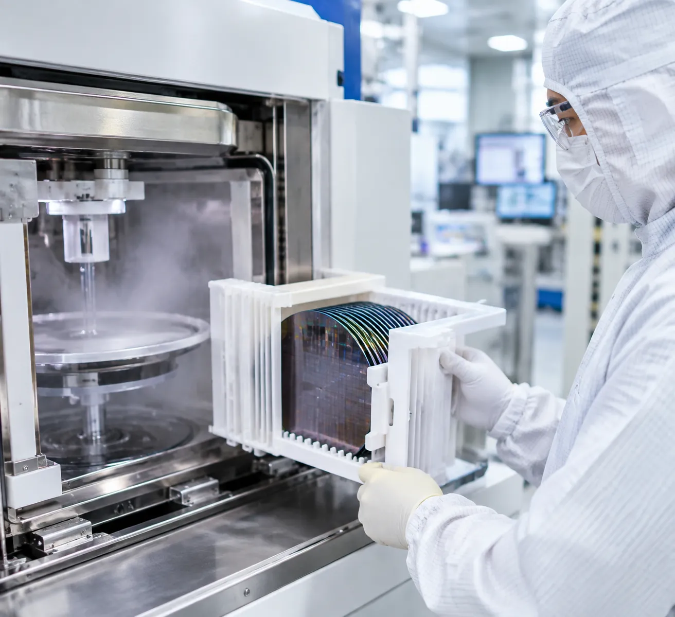
Marangoni and IPA Vapor Drying for High-Aspect-Ratio Features
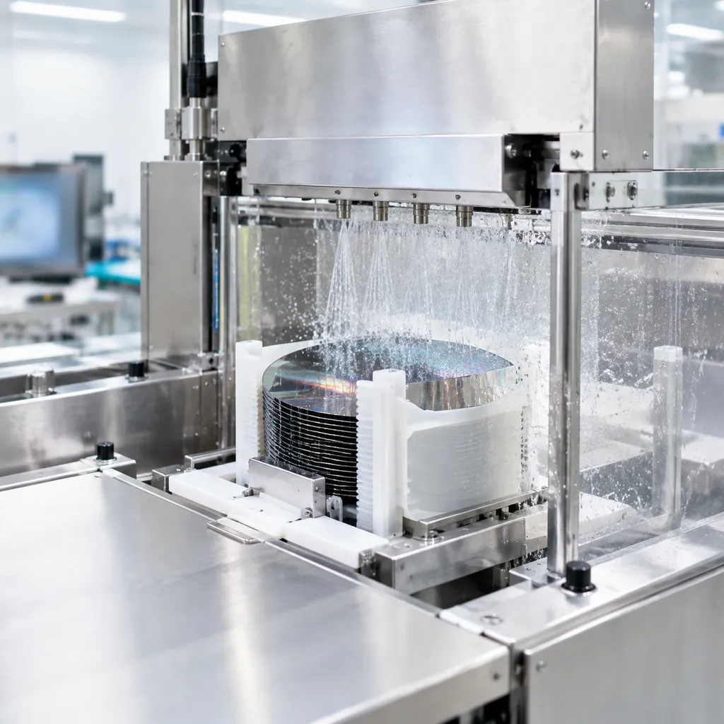
Our integrated Marangoni dryer semiconductor modules create a controlled surface tension gradient at the liquid-gas-substrate interface. By introducing an ultra-dilute isopropyl alcohol (IPA) vapor stream mixed with heated, high-purity N2 during slow wafer withdrawal, we strip deionized water uniformly without mechanical stress.
-
- Capillary Force Elimination: Drastically lowers fluid surface tension to prevent structural stiction in HAR logic and 3D NAND pillars.
- Controlled Chemical Delivery: Ultra-precise vapor metering supported by high-purity pneumatic diaphragm valves prevents chemical pooling and trace residues.
- Optimized Recipe Control: Configurable lift speeds ranging from 0.1 to 5.0 mm/s to match specific hydrophobic/hydrophilic surface transitions.
Sub-Surface Boundary Layer Extraction to Prevent Pattern Collapse
Drying high-density microstructures requires removing trapped boundary layer fluids before vapor exposure. Our drying chambers use active fluid displacement and sub-surface extraction to draw chemistry directly away from trenches, eliminating the micro-droplets that form drying spots.
| Drying Feature | Standard Spin-Rinse Dryer | Our Advanced Marangoni / IPA Vapor Dryer |
|---|---|---|
| Watermark Risk | Moderate to High (due to droplet formation) | Zero Watermarks (100% surface extraction) |
| Pattern Collapse Threshold | Aspect Ratios < 5:1 | Aspect Ratios > 20:1 (Safe) |
| Particle Adders (@ ≥26nm) | > 30 particles per pass | < 5 particles per pass (Ultra-low) |
| IPA Consumption per Run | High volume liquid dispense | Ultra-low closed-loop vapor dosing |
Surface Defect Mitigation and Ultra-Low Particle Adder Control
Our wafer surface preparation equipment isolates the drying chamber from ambient cleanroom turbulence to prevent particulate readsorption. By combining static charge neutralization, dynamic laminar N2 sweeps, and non-contact substrate grippers, our wet etch systems maintain baseline particle counts across raw silicon, polished wafers, and patterned substrates.
Semiconductor Wet Etch Tool Technical Specifications
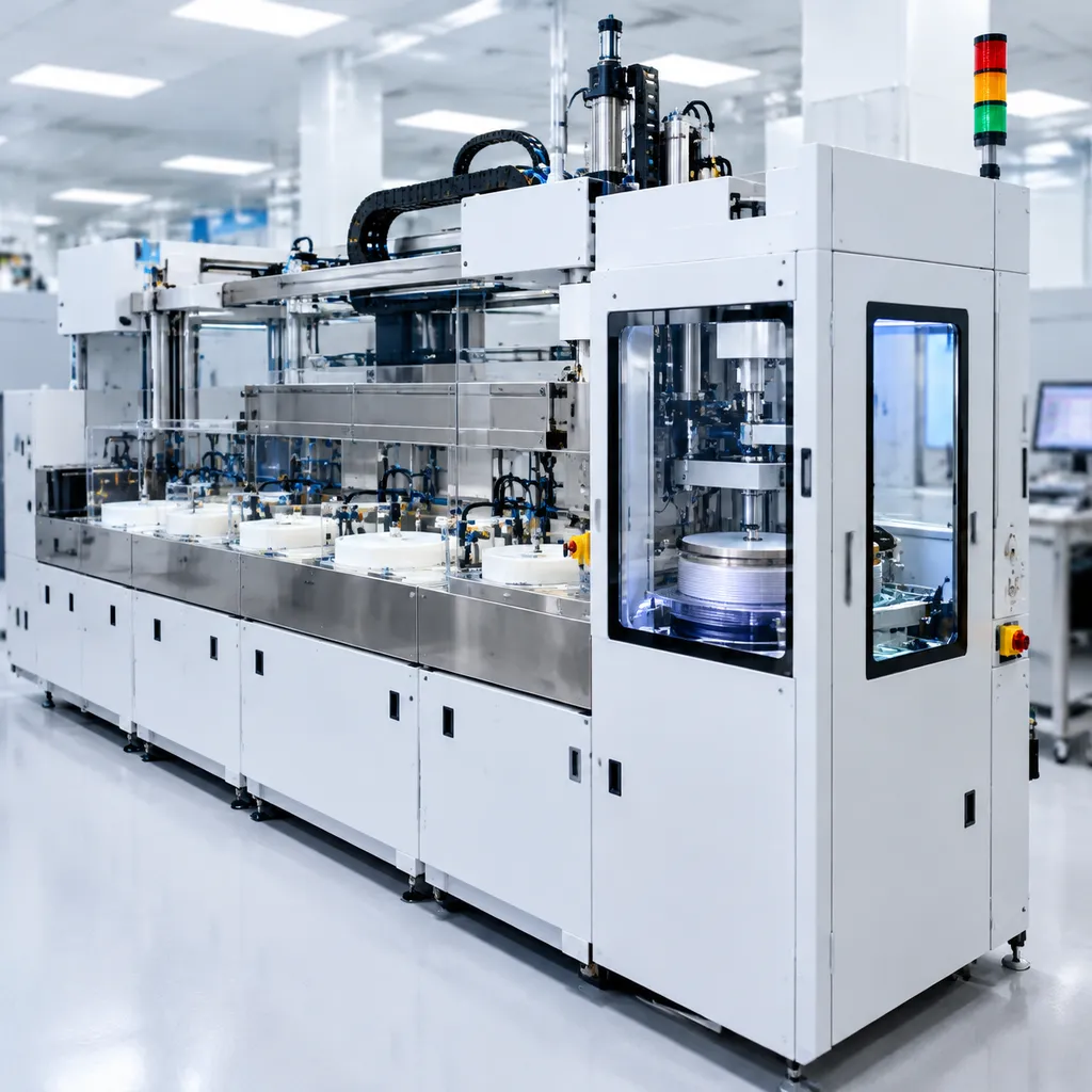
Batch vs. Single-Wafer Platform Comparison
Choosing the right architecture depends on balancing raw volume against critical layer control. We configure our systems to meet specific fab throughput and process targets. For detailed architectural tradeoffs, review our batch immersion vs. single-wafer wet processing comparison.
| Feature / Metric | Automated Batch Wet Bench | Single-Wafer Precision Station |
|---|---|---|
| Primary Use Case | High-volume stripping, bulk oxide etch, pre-diffusion clean | Critical gate etch, single-side etching, thin-film uniformity |
| Wafer Sizes | 100mm, 150mm, 200mm, 300mm | 150mm, 200mm, 300mm |
| Throughput | Up to 180 – 250 wph (carrier-based) | Up to 35 – 50 wph per chamber |
| Etch Uniformity (WIW) | < 1.5% (1-sigma) | < 1.0% (1-sigma) |
| Particle Adder Target | < 15 ea @ ≥ 0.04 µm | < 5 ea @ ≥ 0.02 µm |
| Chemical Flow Mode | Recirculated immersion with POU filtration | Dynamic single-pass dispense or recirculated spray |
Process Uniformity and Thermal Stability
Controlling process variation prevents yield drops across wafer lots. Every wet etch tool semiconductor platform we build features closed-loop thermal and fluid monitoring:
-
- Bath Temperature Stability: Maintained within ±0.5°C across operating ranges from 20°C up to 180°C (hot phosphoric acid).
- Within-Wafer Uniformity (WIW): Sub-1.5% for standard oxide etch via precision fluid injection manifolds and continuous fluid displacement.
- Wafer-to-Wafer (WTW) Repeatability: Tight tolerance monitoring with automated spiked chemical dosing keeps WTW deviation under 1.0%.
- Point-of-Use Chemical Monitoring: Inline real-time refractometers and conductivity sensors detect concentration shifts instantly.
SECS/GEM and Fab Automation Integration
Our semiconductor wet bench cleanroom systems integrate directly into your host network for full lights-out fab operation:
-
- SEMI Standards Compliance: Native support for SECS/GEM (E4, E5, E30, E37) and GEM300 (E39, E40, E87, E90, E94) communication standards.
- Traceability and Logging: Complete lot-level and wafer-level recipe tracking, chemical bath history, alarm logging, and real-time sensor telemetry.
- Automated Material Handling: Automated load port options for FOUP, SMIF, and open cassette loading with dual-end-effector robotic transfer arms.
Supported Fabrication Applications and Semiconductor Nodes
Our wet etch tool semiconductor platform handles demanding etch chemistries and surface preparation tasks across high-volume manufacturing lines. We tune flow dynamics, chemical concentration, and bath temperatures to deliver repeatable process margins across diverse substrate architectures.
| Process Domain | Target Application | Key Chemistries & Performance |
|---|---|---|
| FEOL (Front-End of Line) | Gate Oxide Clearing & Nitride Strip | Hot H₃PO₄, DHF, BOE; >50:1 Si₃N₄:SiO₂ |
| BEOL (Back-End of Line) | Under-Bump Metallization & Pad Etch | Acidic metal etchants (Cu, Al, Ti) |
| Power & MEMS | Bulk Micromachining & Sacrificial Release | KOH, TMAH, HF; zero-stiction drying |
| Advanced Packaging | TSV Residue Strip & Micro-Bump Clean | Solvent/acid blends, megasonic assist |
FEOL Gate Oxide Clearing and Selective Nitride Strip
-
- High-Selectivity Nitride Stripping: Hot phosphoric acid baths maintain precise boiling points and silicon spiking levels to deliver consistent >50:1 selectivity to thermal oxide.
- Gate Oxide Pre-Cleans: Controlled dilute HF (DHF) and buffered oxide etch (BOE) chemistries strip native and sacrificial oxides without pitting silicon surfaces.
- Sub-Nanometer Uniformity: Recirculating bath hydrodynamics maintain continuous flow over both sides of the wafer during critical wafer fabrication steps.
BEOL Under-Bump Metallization and Pad Etching
-
- Controlled Metal Recess: Specialized chemical delivery systems etch Ti, Cu, Ni, and Al barrier layers cleanly while preventing galvanic corrosion.
- Lateral Undercut Control: Dynamic fluid delivery avoids over-etching under contact pads and ensures trace integrity across fine-pitch metal layers.
- Post-Etch Residue Clearing: Integrated rinse sequences eliminate polymer residues and chemical traces before subsequent dielectric deposition.
Power Electronics and MEMS Bulk Micromachining
-
- Anisotropic Silicon Etching: Heated KOH and TMAH stations etch precise geometric cavities, diaphragms, and V-grooves along crystallographic planes.
- Sacrificial Layer Release: High-precision isotropic oxide release modules free suspended MEMS beams and micro-structures without mechanical damage.
- Compound Semiconductor Processing: Dedicated containment baths handle aggressive acid formulations for wide-bandgap SiC and GaN surface etching.
Advanced Packaging TSV Cleaning and Micro-Bump Preparation
-
- High-Aspect-Ratio TSV Wetting: Point-of-use megasonic agitation drives chemistry into deep Through-Silicon Vias (TSVs) to clear post-DRIE fluoropolymer residues.
- Micro-Bump Surface Prep: Fluxless oxide removal and copper-pillar cleaning steps prepare micro-bumps for void-free thermo-compression bonding.
- High-Density Packaging Integration: Our stations support thin-wafer and carrier-mounted substrate processing essential for advanced semiconductor packaging flows.
Cleanroom Safety, Fire Retardancy, and Chemical Containment
Operator safety, strict contamination control, and comprehensive risk mitigation dictate how we design every wet etch tool semiconductor platform. Corrosive chemistries and high-temperature baths demand robust structural containment, dependable exhaust mechanisms, and real-time fault responses to safeguard fab operations and maintain uninterrupted production.
FM4910 Certified Fluoropolymer Construction
To mitigate fire risks and eliminate ionic leaching in aggressive chemical environments, our systems are built from top-grade, flame-retardant materials:
-
- Material Integrity: Constructed using FM4910-listed PVDF, ECTFE, and PTFE to ensure zero combustion propagation and maximum chemical inertness.
- Corrosion Resistance: High resistance against hot phosphoric acid, hydrofluoric blends, and solvent chemistries ensures long tool lifespans without structural degradation.
- Compliance Standards: Fully compliant with SEMI S2, S8, and CE standards for cleanroom safety and ergonomic operation.
Our acid wet bench for safe chemical processing integrates these certified plastics to guarantee maximum chemical resistance alongside strict cleanroom compliance.
| Safety Metric | System Specification | Fab Benefit |
|---|---|---|
| Material Fire Rating | FM4910 Certified Plastics (PVDF) | Zero fire spread risk in cleanroom |
| Exhaust Flow Control | Dynamic Push-Pull Laminar Flow | Prevents vapor escape into worker zone |
| Leak Detection Response | Triple-Redundant Optical & Float | < 500 ms automatic line isolation |
| Emergency Chemical Dump | Gravity-Assisted Fail-Safe Dump | Safe bath evacuation in power outage |
Dynamic Push-Pull Fume Evacuation and Laminar Flow
Controlling chemical vapors at the bath surface protects cleanroom personnel and preserves process stability:
-
- Push-Pull Aerodynamics: Balanced laminar air knives push micro-fumes directly into high-velocity lip exhausts, preventing corrosive vapor migration into the fab.
- Exhaust Optimization: Factory facility tie-ins connect smoothly with facility chemical exhaust scrubbers to maintain steady static pressure and lower overall fab HVAC loads.
- Mini-Environment Isolation: Sealed processing zones feature HEPA/ULPA filtration to eliminate airborne molecular contamination (AMC) above open chemical baths.
Automated Leak Detection and Redundant Emergency Dumps
Our multi-layered interlock network continuously monitors process health to handle potential leaks immediately:
-
- Dual-Containment Basins: All chemical supply lines, valves, and heated tanks rest within secondary containment zones equipped with redundant optical and continuous-loop leak sensors.
- Instant Emergency Drain Interlocks: Automated pneumatic gravity-dump valves instantly route hazardous solutions to segregated neutralizing drain lines upon trigger detection or power loss.
- Hardware Interlock Matrix: Hardwired EMO integration instantly cuts heater power, isolates chemical dispense lines, and increases exhaust draw without relying solely on software loops.
Optimizing Cost of Ownership and Fab Integration
Reducing chemical waste and maximizing cleanroom floor space directly lower your cost per wafer.
Closed-Loop Chemical Replenishment and Bath Lifetime Extension
Chemical consumption is one of the highest recurring operational expenses in wet processing. Our automated replenishment architecture monitors bath chemistry in real time to prevent premature bath dumps.
-
- Real-Time Concentration Monitoring: Integrated inline refractive index and titration sensors track dynamic chemical depletion.
- Precision Micro-Spiking: Automated closed-loop dosing injects precise volumes of chemistry and spiked oxidizers to stabilize etch rates without process drift.
- Bath Lifetime Doubling: Controlled chemical replenishment extends active bath life by up to 300%, significantly lowering chemical purchase and disposal costs.
- Automated Drain Segregation: Dedicated lines separate hazardous chemistries for recycling, neutralization, or waste treatment.
Custom Modular Footprint for Cleanroom Retrofits
Cleanroom floor space comes at a premium. Leveraging our specialized engineering capability, we configure modular frames that fit into tight legacy bays or align with high-throughput automated 300mm fab aisles.
| Design Feature | Engineering Specification | Fab Advantage |
|---|---|---|
| Footprint Layout | Modular linearly expandable bays | Up to 30% floor space savings |
| Utility Interconnects | Top, bottom, or side-entry facility routing | Drop-in replacement for legacy wet benches |
| Maintenance Access | 100% front and rear service access panels | Zero required side clearance between tools |
| Platform Compatibility | Manual, semi-automated, and fully automated OHT | Seamless interface with automated fab logistics |
Our flexible wet bench chemistry equipment for semiconductor cleanroom facilities enables clean drop-in upgrades without requiring costly floor grid modifications or utility rebuilds.
Global Field Service, Preventative Maintenance, and Engineering Support
Tool availability depends on reliable maintenance and rapid on-site support. We back our wet etch equipment with a global response network focused on maximizing tool uptime and mean time between failures (MTBF).
-
- Standardized PM Kits: Pre-packaged seal, valve, and filter replacement kits streamline scheduled preventative maintenance.
- Fast MTTR Performance: Quick-disconnect manifolds, modular pump carts, and accessible electronics keep Mean Time to Repair (MTTR) under 2 hours for common wear items.
- 24/7 Global Engineering Access: Direct access to our process and field service engineers for recipe optimization, troubleshooting, and tool commissioning.
- Predictive Telemetry: SECS/GEM integrated data logging flags component wear and pump performance deviations before catastrophic failures occur.
Frequently Asked Questions About Semiconductor Wet Etch Tools
What is the difference between automated batch and single-wafer wet etching?
Choosing between batch and single-wafer architectures comes down to balancing throughput against individual wafer process control.
| Feature | Automated Batch Wet Benches | Single-Wafer Precision Tools |
|---|---|---|
| Throughput | High (Up to 50 wafers per run) | Moderate (Wafer-by-wafer processing) |
| Best Used For | Bulk oxide removal, RCA cleans, nitride strip | Critical layer etching, ultra-thin films, R&D |
| Footprint Efficiency | Maximized chemical bath utilization | Dedicated chamber per wafer |
| Process Control | Cassette-wide thermal uniformity | Individual front/backside recipe control |
Our automated wet bench semiconductor wet processing systems deliver massive volume cost advantages, while single-wafer tools provide pinpoint chemical delivery for the most sensitive device layers.
How does the tool achieve sub-1.5% within-wafer etch uniformity?
We eliminate edge-to-center boundary layer variations by combining three core engineering controls:
Precision Recirculation Weir Design: Continuous overflow weirs maintain constant bath velocity and eliminate dead zones across the tank.
Inline Chemical Spiking: Automated spiking systems replenish consumed active reagents in real time, preventing concentration decay.
Dynamic Fluid Agitation: Tuned chemical agitation prevents stagnant boundary layers at the substrate surface, ensuring consistent etch rates across entire 200mm and 300mm wafers.
Which acid chemistries are compatible with high-temperature processing?
Our wet etch tool semiconductor platforms utilize high-purity PVDF, PFA, and quartz process tanks engineered to handle aggressive acids at sustained elevated temperatures:
Hot Phosphoric Acid (H3PO4): Operates up to 160°C – 180°C with automated DI water spiking for selective silicon nitride stripping over silicon oxide.
Sulfuric Acid & Hydrogen Peroxide Mixtures (SPM/Piranha): Sustains 120°C – 150°C for organic photoresist removal and surface preparation.
Buffered Oxide Etch (BOE / BHF): Controlled ambient to elevated baths for precise, damage-free isotropic silicon dioxide etching.
Hydrochloric & Nitric Acid Blends: Multi-chemical capability for compound semiconductor gate recessing and metal clearing.
For specialized dielectric removal, our high-precision wet benches for semiconductor processing ensure reliable bath thermal stability within ±0.5°C across all chemical profiles.
How does Marangoni drying eliminate watermarks on fragile microstructures?
Watermarks form when droplet evaporation leaves behind dissolved silica or ionic contaminants. Our Marangoni drying modules eliminate this mechanism completely:
Surface Tension Gradient: An ultra-low concentration isopropyl alcohol (IPA) vapor stream is introduced at the nitrogen-liquid interface as the wafer is slowly lifted from the DI water rinse tank.
Capillary Pull: The alcohol creates a surface tension gradient (the Marangoni effect) that actively pulls water off the hydrophilic and hydrophobic surfaces.
Zero Droplet Residue: Liquid sheets off continuously without breaking into individual droplets, leaving patterns completely dry and eliminating pattern collapse on sub-micron, high-aspect-ratio features.