Are you looking to eliminate micro-contamination and dramatically boost your semiconductor yield?
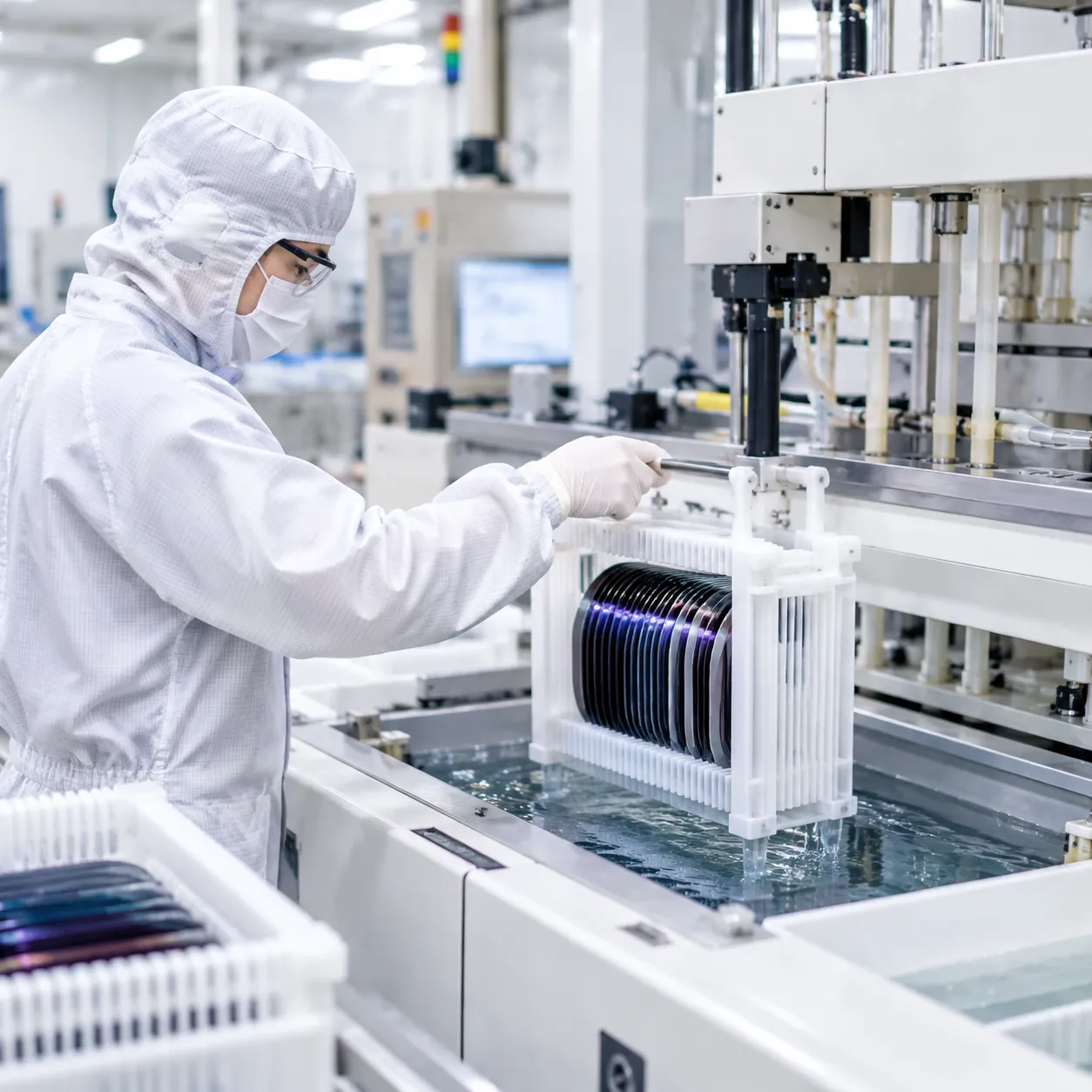
As device nodes continue to shrink, conventional batch processing simply can't deliver the precision you need. That is where advanced single wafer wet clean technology changes the game.
Getting it right means superior defect control, zero cross-contamination, and unmatched process uniformity on every single run.
In this comprehensive guide, you'll learn the core mechanisms, chemical formulations, and practical strategies behind modern single wafer wet clean processes—giving you actionable insights based on real fab experience.
Let’s dive right in.
Fundamental Mechanisms of Single Wafer Wet Cleaning
Single wafer wet clean systems leverage synchronized chemical reactions, fluid dynamics, and surface tension manipulation to achieve single-nanometer defect control.
Chemical Dissolution and Surface Oxidation Mechanisms
Chemical cleaning in single-wafer processing relies on sequential oxidation, etching, and metal chelation cycles. Fresh chemistry dispensed onto a rotating wafer surface accelerates reaction kinetics compared to stagnant batch baths.
| Chemistry Formulation | Primary Function | Target Contaminants | Core Reaction Mechanism |
|---|---|---|---|
| SC-1 (NH₄OH / H₂O₂ / DIW) | Organic removal & particle lift-off | Light organics, Si particles | Micro-etching of silicon substrate combined with continuous surface re-oxidation; negative zeta potential generation. |
| SC-2 (HCl / H₂O₂ / DIW) | Metallic impurity stripping | Trace alkali & transition metals (Fe, Cu, Al) | Formation of soluble metal chloride complexes in an acidic, oxidizing regime. |
| DHF (Dilute HF, 1:100 to 1:1000) | Native/thermal oxide etching | Surface metallic ions trapped in oxide | Direct dissolution of silicon dioxide (SiO₂ + 6HF → H₂SiF₆ + 2H₂O), leaving a hydrogen-terminated hydrophobic surface. |
| SPM (Piranha: H₂SO₄ / H₂O₂) | Heavy organic & photoresist stripping | Heavy carbon residues, hardened resists | High-temperature oxidation via peroxymonosulfuric acid (H₂SO₅) formation. |
| DIO₃ (Ozonated DI Water) | Low-loss organic stripping | Surface organics, thin native oxide growth | Hydroxyl and oxygen radical-driven oxidation with zero chemical residue. |
Physical Energy Transfer and Boundary Layer Thinning
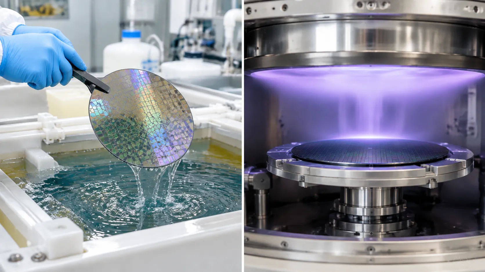
Chemical etching alone cannot dislodge sub-20nm particles trapped in the stagnant fluid layer. We utilize high-speed wafer rotation combined with directed acoustic fields to drastically thin the hydrodynamic boundary layer.
-
- Boundary Layer Compression: Centrifugal force thins the viscous boundary layer ($\delta$) down to sub-micron dimensions, enabling active chemical species to access tight trench geometries.
- Schlichting Streaming: Acoustic boundary layers generate localized secondary fluid eddies near the wafer surface, creating high localized shear stress.
- Eckart Streaming: Bulk acoustic wave propagation creates bulk fluid circulation that rapidly carries dislodged particles out of high-aspect-ratio (HAR) trenches into the waste stream.
Acoustic Cavitation Control to Suppress Fine-Pattern Damage
Uncontrolled acoustic cavitation generates transient micro-bubbles that violently collapse, causing catastrophic structural collapse in advanced nodes. Our process designs enforce precise megasonic energy management:
-
- Stable Cavitation Management: We operate acoustic transducers within frequency bands of 0.8 MHz to 3.0 MHz, favoring stable, low-amplitude bubble oscillation over destructive transient cavitation.
- Uniform Power Distribution: Pulsed-wave megasonics and acoustic beam scanning prevent localized energy hot-spots across the wafer radius.
- Defect-Free Cleaning Threshold: By keeping physical shear stresses precisely between the particle removal threshold and the pattern fracture limit, we achieve >98% PRE on sub-30nm contaminants with zero gate or fin deformation.
Advanced Rinsing Dynamics and Marangoni Surface Tension Drying
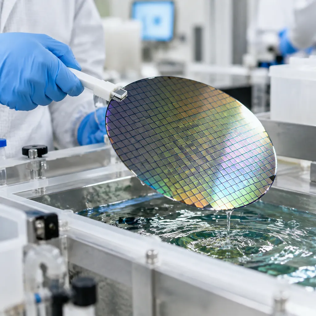
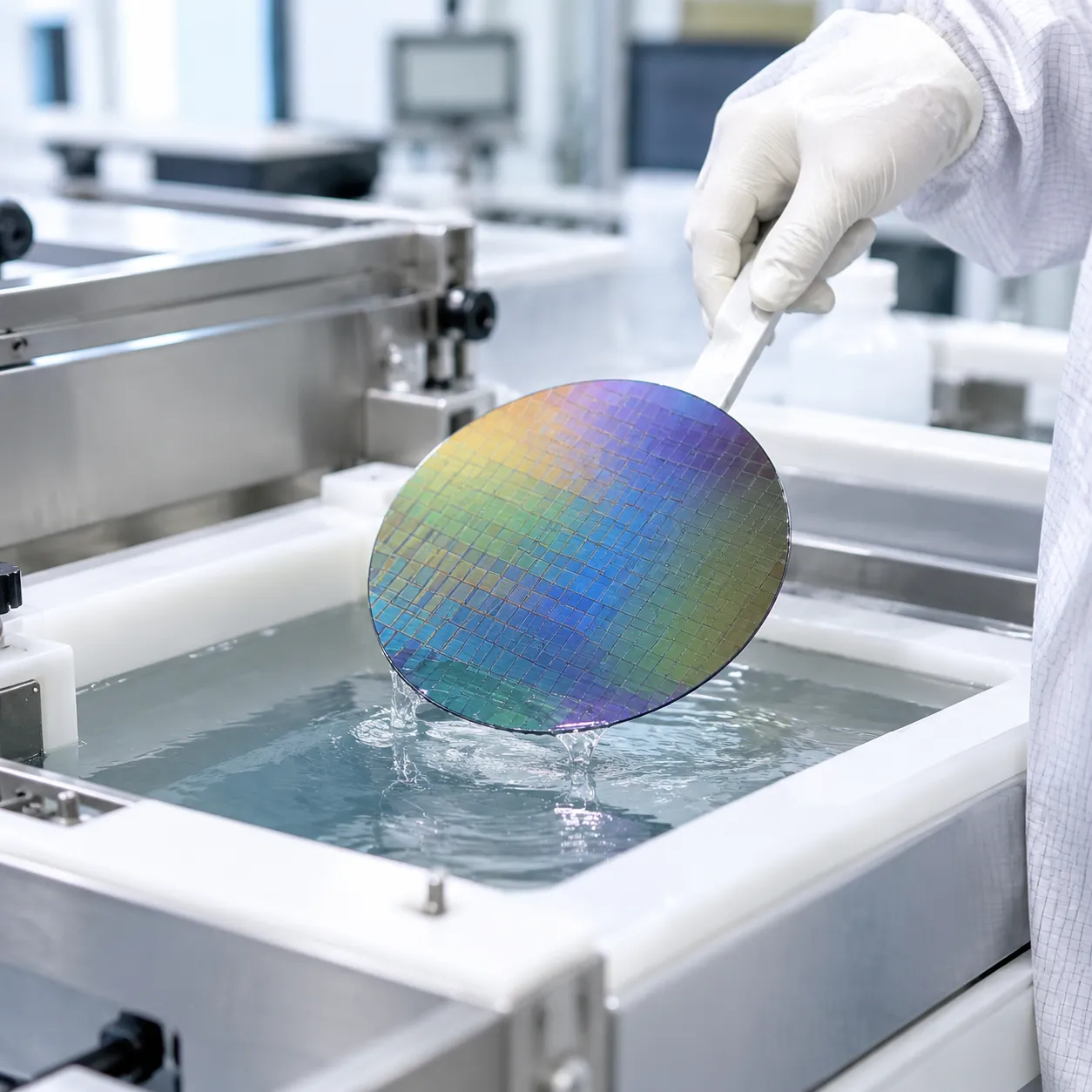
The transition from chemical treatment to dry surface is the most critical window for watermark and residue formation. We eliminate residual chemical entrapment and drying defects through integrated Marangoni processing.
[ IPA Vapor + N2 Carrier Flow ]
|
v
================================================== <-- Low Surface Tension Zone
\ \ \ \ \ \ \ \ \ \ \ \ \ \ \ \
\ \ \ \ \ DIW Water Film \ \ \ \ \ <-- High Surface Tension Zone
==================================================
[Wafer Surface]
- Deionized Water (DIW) Quick-Displacement: High-flow DIW injection nozzles flush chemistry from the center out, clearing the wafer in seconds.
- Surface Tension Gradients (Marangoni Effect): Injecting an Isopropyl Alcohol (IPA) vapor and nitrogen (N₂) mixture at the receding edge of the DIW rinse creates a sharp surface tension gradient (Δγ).
- Capillary Force Neutralization: The Marangoni force pulls liquid away from hydrophobic structures into the bulk droplet, preventing liquid trapping inside micro-trenches.
- Watermark Elimination: Rapid, evaporation-free liquid retraction suppresses the formation of silicic acid (H₂SiO₃) precipitates and drying stains.
Single Wafer Wet Clean vs. Batch Wet Bench
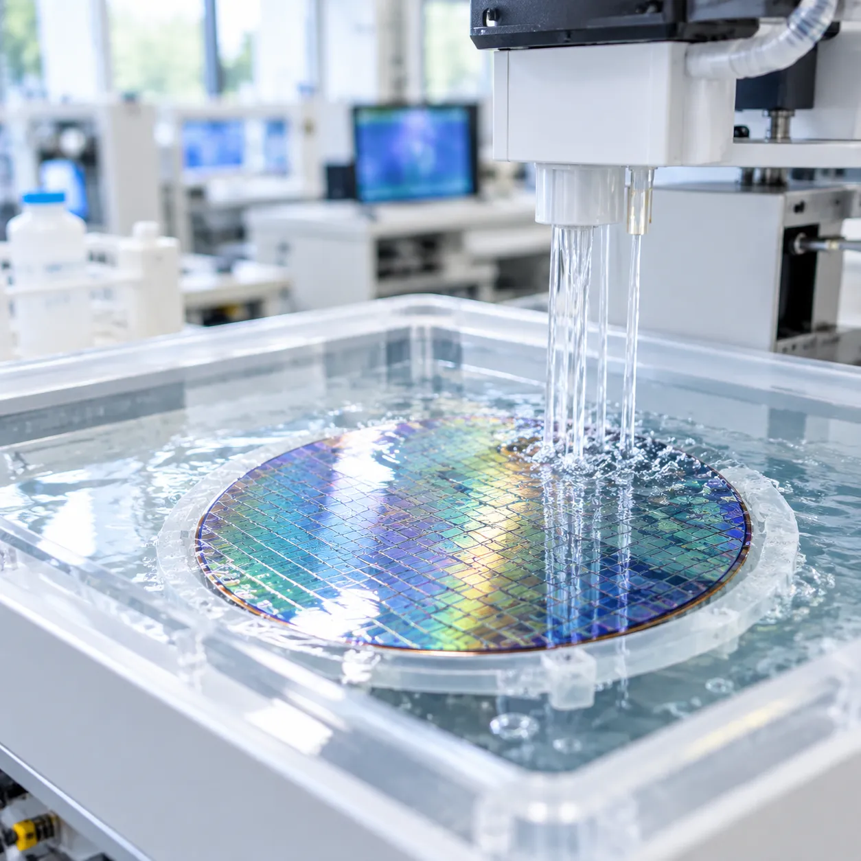
Choosing between a single wafer wet clean platform and an immersion batch system comes down to your node requirements, defect budget, and yield targets. While immersion systems still handle high-throughput bulk steps well, advanced nodes demand a level of precision that tanks simply cannot deliver.
| Metric | Single Wafer Wet Clean | Batch Wet Bench |
|---|---|---|
| Process Uniformity | Dedicated dispense, wafer center-to-edge tuning (<1% non-uniformity) | Fluid flow gradients across carrier boats (3–5% variance) |
| Cross-Contamination | Zero risk; single-pass fresh chemical chemistry | High risk; particle build-up and bath chemical loading over cycles |
| Defectivity / PRE | Superior on sub-200 nm particles using physical force assistance | Prone to redeposition on outer/inner carrier positions |
| Chemical Economics | High chemical consumption; requires point-of-use reclaim | High volume per bath, but low cost-per-wafer via recirculation |
| Best Use Case | Critical FEOL/BEOL, HAR structures and high-aspect gate etching | Non-critical bulk strip, reclaim, and thick oxide etching |
Process Uniformity and Wafer-to-Wafer Repeatability
When processing sub-200nm structures, immersion tanks hit physical limits. In a tank, wafers sitting on the edges of the boat experience different fluid velocities and boundary layers than those packed tightly in the center.
By contrast, our single wafer wet processing equipment for 300mm fabs spins each substrate individually while delivering fresh chemical blends through a sweeping dynamic arm. This setup delivers exact boundary layer control, eliminates flow dead zones, and drops wafer-to-wafer etch rate variation down to negligible levels across the entire lot.
Eliminating Chemical Bath Cross-Contamination
Batch processing creates an inherent defect trade-off: every wafer loaded into a shared tank deposits particles, trace metals, and chemical byproducts directly into the solution. Even with continuous bath filtration and fluid turnover, redeposition remains a primary yield killer.
-
- Single-Pass Chemistry: Fresh, uncontaminated chemistry contacts the wafer surface every time, preventing back-end trace metal migration.
- Controlled Chamber Environment: Individual mini-chambers isolate volatile chemistries, preventing atmospheric exposure and unwanted vapor migration.
- Dedicated Drain Architecture: We route incompatible chemistries into segregated reclaim or neutralization drains, ensuring zero cross-mixing between process sequences.
Balancing Chemical Consumption and Process Economics
Single-pass cleans use dynamic recipe timing to balance chemical usage against yield gains. Running fresh chemicals for every single wafer increases consumable consumption compared to a traditional chemical wet bench for wafer cleaning and etching, which re-circulates chemistries over dozens of production runs.
To keep the cost of ownership (CoO) lean, we cut recipe cycle times using localized chemical heating at the point of use (POU) and dial in micro-dispense flows. Concentrated chemical injection combined with dynamic DI water dilution reduces chemical footprints without degrading the particle removal efficiency (PRE).
Application Matrix: Matching Tools to Critical Process Steps
Not every process step justifies the single wafer footprint. Determining the right tool architecture requires matching wafer topography and yield sensitivity to the equipment platform:
-
- Front-End-of-Line (FEOL) Critical Cleans: Single wafer wet clean is non-negotiable for pre-gate dielectric cleans, fin cleans, and shallow trench isolation (STI) steps where material loss must stay below 0.1 nm.
- Back-End-of-Line (BEOL) Post-Etch Cleans: Dual-side single wafer processing completely strips stubborn post-fluorinated polymer residue from high-aspect-ratio (HAR) contact vias without pitting underlying barrier metals.
- Bulk Cleans and Strips: Immersion wet benches remain the top choice for bulk photoresist stripping, wafer reclaim, initial incoming wafer degreasing, and non-critical pad oxide etching where high batch throughput drives fab margins.
Core Subsystems and Hardware Architecture in Single Wafer Wet Clean
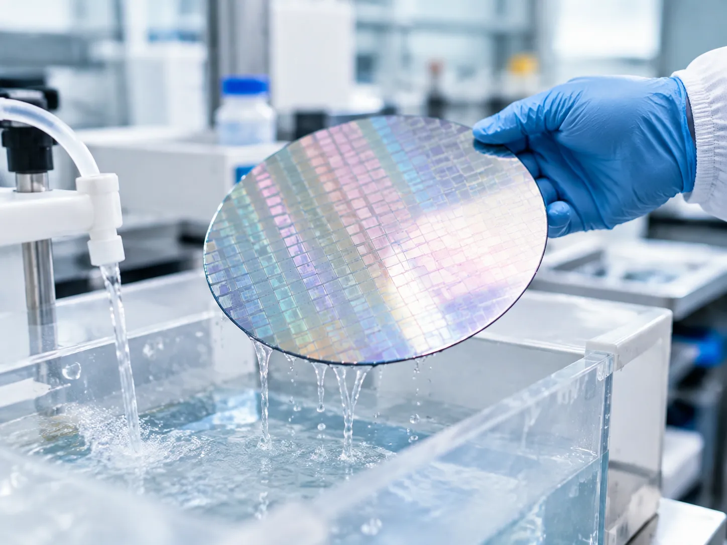
Dynamic Chemical Dispense and Point-of-Use (POU) Heating
Standard delivery loops introduce chemical aging and heat loss. To eliminate thermal gradients across the substrate, we position high-speed dispense arms combined with in-line, point-of-use (POU) infrared heaters directly upstream of the nozzle:
-
- Dynamic Scan Velocity: Dispense arms use programmable, non-linear sweep profiles to match linear velocity increases from wafer center to edge, maintaining uniform chemical residence time.
- Closed-Loop POU Temperature Control: POU heating brings active mixtures like dilute SC-1 or SPM to target temperatures (up to 80°C–140°C) in seconds, mitigating chemical decomposition before the fluid hits the surface.
- Multi-Nozzle Configuration: Dedicated fluid lines for acids, bases, and ultra-pure water (UPW) prevent cross-line salt precipitation and line-clogging.
Chamber Isolation and Multi-Bowl Chemical Recovery
Cross-contamination between incompatible chemistries destroys yield. Our chemical cleaning equipment uses segmented, multi-tier process bowls and dynamic splash guards to handle chemical shifts within seconds.
| Subsystem Component | Engineering Function | Fab Process Benefit |
|---|---|---|
| Multi-Level Stacked Bowls | Pneumatically actuated vertical bowl switching based on dispense recipe step. | Zero cross-contamination between acidic (DHF) and basic (SC-1) solutions. |
| Segregated Chemical Reclaim | High-efficiency separation tracks reclaimable chemistries (e.g., SPM) from non-reclaimable fluids. | Reduces fab chemical consumption and operating cost. |
| Multi-Zone Exhaust Balancing | Direct routing of acid, solvent, and alkaline vapors to dedicated chemical exhaust scrubbers. | Prevents toxic vapor mixing and maintains chamber pressure stability. |
Inert Gas Mini-Environments to Suppress Dissolved Oxygen
Hydrophobic silicon surfaces are prone to rapid native oxide growth and watermark formation if exposed to ambient air during wet cleans.
-
- Nitrogen Sealed Enclosures: We encapsulate the process chamber in a continuous positive-pressure nitrogen ($N_2$) curtain, driving ambient oxygen levels down below 10 ppm.
- Degassed UPW Injection: Deoxygenated UPW systems lower dissolved oxygen (DO) to under 1 ppb, eliminating galvanic corrosion on exposed metal gates and stopping localized etch pit formation dead in its tracks.
Wafer Backside and Bevel Cleaning with Bernoulli Chucking Systems
Non-contact handling is critical for preserving pristine frontside patterns during aggressive backside strip and bevel cleans:
-
- Bernoulli Chuck Mechanics: By directing high-velocity nitrogen across the chuck face, we create a controlled low-pressure zone directly beneath the wafer. The wafer floats securely on an inert gas cushion without mechanical contact on critical device areas.
- Backside-to-Frontside Chemical Isolation: A continuous nitrogen or UPW frontside barrier flow prevents acid creep or chemical mist from wrapping around the wafer edge during bevel etching.
- Edge-Bevel Rinse (EBR) Nozzles: Precision micro-dispense nozzles target the bevel exclusion zone (down to 0.5 mm from the wafer edge), stripping metallic contaminants, edge-bead polymers, and flaking films to prevent defect migration back into the active die area.
Process Optimization and Defectivity Mitigation
In advanced front-end-of-line (FEOL) wet cleaning, optimizing process windows requires balancing particle removal against material loss and structural integrity. Our advanced wet process technology addresses these competing requirements by precisely tuning physical forces, chemistries, and environmental controls.
| Critical Challenge | Primary Mechanism | Engineering Solution |
|---|---|---|
| Pattern Collapse | Cavitation shear stress | High-frequency megasonics (>1 MHz) |
| Thin Film Material Loss | Uncontrolled chemical etch | Ultra-dilute SC-1 / cold DHF |
| Watermark Defects | O₂ + DIW dissolution (H₂SiO₃) | N₂-purged IPA Marangoni drying |
| Silicon Pitting / Ra | OH⁻ attack on pure Si | Dissolved O₂ & pH ratio control |
Maximizing Particle Removal Efficiency (PRE) Without Pattern Destruction
Achieving >99% Particle Removal Efficiency (PRE) on sub-20nm particles without breaking high-aspect-ratio (HAR) patterns demands fine-tuned acoustic streaming.
-
- Frequency Tuning: We deploy multi-frequency megasonic transducers (1.0 to 3.0 MHz) to minimize violent transient cavitation while maintaining strong acoustic micro-streaming within dense pattern trenches.
- Acoustic Power Density: Operating at low power densities (0.5–1.2 W/cm²) thins the hydrodynamic boundary layer sufficiently to dislodge nanoscale contaminants without exerting destructive lateral shear force on sensitive FinFET or gate-all-around (GAA) structures.
Minimizing Material Loss on Thin Dielectrics and High-k Metal Gates
Aggressive cleaning chemistries can quickly strip ultra-thin gate oxides, SiN spacers, and high-k metal gate (HKMG) materials.
-
- Ultra-Dilute Formulations: We switch conventional Standard Clean 1 (SC-1) and dilute hydrofluoric acid (DHF) to ultra-dilute regimes (e.g., 1:1:100 to 1:1:500 for APM) to lower silicon dioxide etch rates to <0.1 Å/min.
- Dynamic Point-of-Use Dosing: Through precise chemical process management, chemical delivery stays within exact millisecond contact windows and strict temperature thresholds (15°C to 25°C for sensitive etching steps) to stop unwanted oxide loss.
Watermark Defect Prevention on Hydrophobic Surfaces
Stripping native oxides with DHF exposes bare hydrophobic silicon, which is vulnerable to dissolved oxygen-induced watermarks ($H_2SiO_3$ residue).
-
- Inert Processing Environment: We run DHF etch and subsequent DI water rinse cycles under a sealed, nitrogen-purged mini-environment, dropping ambient oxygen levels below 10 ppm.
- Surface Tension Gradient Drying: Applying an isopropyl alcohol (IPA) vapor-nitrogen mixture immediately after rinsing drives Marangoni surface tension drying. This pulls water droplets off the wafer face before evaporation can trigger silicon etching or watermark formation.
Surface Micro-Roughness (Ra) and Silicon Pitting Control
Uncontrolled alkaline cleans attack exposed silicon along crystal planes, causing surface micro-roughness (Ra) degradation and destructive pitting.
- Redox Potential & pH Balancing: By adjusting the NH₄OH : H₂O₂ : H₂O stoichiometric ratios, we keep the surface continuously passivated with a protective, sub-nanometer chemical oxide layer during particulate scrub cycles.
- Dissolved Gas Management: Degassing DI water to strip dissolved oxygen (DO < 1 ppb) suppresses pitting corrosion on bare silicon and metal layers during extended rinse steps, preserving sub-angstrom surface roughness.
Industrial Equipment Solutions for High-Yield Wet Processing
Yield maximization across modern fabs requires cleanroom hardware that combines extreme chemical flexibility with footprint efficiency. In our wet station semiconductor equipment for wafer processing, we engineer modular processing platforms that eliminate cross-talk while maintaining high-throughput output across diverse substrate matrices.
Modular Single Wafer Architecture
In-Line POU Heating → Multi-Bowl Chemical Segregation → Marangoni Dryer
Multi-Arm Dispense → Inert N₂ Chamber Enclosure → Reclaim / Recycle
Multi-Chemical Integration and Modular Chamber Configurations
Advanced process flows require sequential acid and solvent steps within a single recipe without physical tool transfers. We address this through isolated multi-bowl stack designs:
-
- Dedicated Chemical Manifolds: Independent liquid paths prevent cross-contamination between aggressive etchants (DHF, BOE) and organics/solvents (SPM, solvent strippers).
- Multi-Level Drain Diverters: Dynamic drain routing segregates chemical waste streams in real time, routing valuable chemistries to reclaim loops while sending exhausted solutions to specialized neutralization systems.
- Scalable Chamber Footprints: Cluster configurations allow flexible 4-chamber, 8-chamber, or 12-chamber integration with high-speed dual-end-effector robotic wafer handling.
Seamless equipment integration ensures our single wafer processor setups communicate directly with fab-wide automated material handling systems (AMHS) to prevent bottlenecks during recipe changeovers.
Processing Compound Semiconductors: SiC and GaN Alongside Silicon
Compound semiconductors present unique structural challenges compared to standard silicon, including extreme chemical resistance, transparent substrate handling, and high surface hardness:
| Substrate Material | Primary Wet Clean Challenges | Our Hardware & Process Solutions |
|---|---|---|
| Silicon (Si) | Pattern collapse, watermark formation on hydrophobic surfaces | Megasonic boundary-layer thinning + IPA Marangoni drying |
| Silicon Carbide (SiC) | Heavy sub-surface damage (SSD) removal, inert surface etching | High-temperature SPM/APM dispense + high-force spin etching |
| Gallium Nitride (GaN) | High defect density, sensitivity to surface pitting | Ultra-precise DHF/alkaline chemical balance with real-time POU dosing |
We utilize specialized non-contact Bernoulli and edge-grip chucking systems to handle warped, transparent, or ultra-thin SiC and GaN substrates without micro-cracking or front-side contact defects.
Green Fab Integration and Lowering Cost of Ownership (CoO)
Balancing environmental sustainability with fab operating costs requires direct reduction of chemical, gas, and utility usage:
-
- Single-Pass Chemical Minimization: High-precision dispense nozzles deliver target flow rates under 0.8 to 1.2 L/min, drastically reducing virgin chemistry demand compared to traditional immersion tanks.
- In-Line DIW and Chemical Reclamation: Integrated sensors analyze effluent purity to divert reusable rinse water back to the fab's primary reclaim plant.
- Reduced Exhaust Footprint: Enclosed mini-environment chambers lower cleanroom HVAC and exhaust demand by pulling localized air volumes only during active chemical delivery.
Frequently Asked Questions About Single Wafer Wet Clean
Why switch from batch wet benches to single wafer wet cleaning systems?
Advanced device scaling and tight node specifications leave zero margin for wafer-to-wafer variance or chemical cross-contamination. While high-throughput batch wafer cleaning systems remain cost-effective for non-critical bulk cleans, leading fabs deploy single wafer cleaning systems for critical Front-End-of-Line (FEOL) and Back-End-of-Line (BEOL) steps.
Processing wafers individually delivers distinct manufacturing advantages:
Zero Cross-Contamination: Fresh chemical chemistry is delivered to every single wafer, eliminating bath particle loading and ionic drift.
Precise Boundary Layer Control: High-speed wafer rotation combined with dynamic nozzle sweeps creates ultra-thin liquid boundary layers, speeding up chemical reaction rates.
Bevel and Backside Isolation: Dedicated chuck designs isolate and clean the wafer edge and backside simultaneously without damaging top-side structures.
How does single wafer processing prevent watermark defects on hydrophobic silicon?
Watermark defects (H₂SiO₃ formation) occur when dissolved oxygen in residual deionized (DI) water reacts with bare silicon surfaces during droplet evaporation. Single wafer wet clean tools eliminate this risk through integrated physical and chemical controls:
- Inert Chamber Mini-Environments: Nitrogen (N₂)-purged process bowls reduce ambient oxygen levels below critical reaction thresholds.
- Advanced Marangoni Drying: An isopropyl alcohol (IPA) vapor and N₂ mixture is applied immediately adjacent to the receding DI water rinse front. The resulting surface tension gradient pulls fluid off hydrophobic surfaces instantly, preventing droplet pinning and evaporation stains.
- High-Speed Fluid Displacement: Centrifugal acceleration sweeps chemical residues outward before drying can occur.
What is the role of megasonic frequency control in avoiding pattern collapse?
High-aspect-ratio (HAR) patterns and fragile gate structures are highly susceptible to mechanical damage caused by violent acoustic cavitation. We manage acoustic energy transfer through tight frequency modulation:
| Control Parameter | Mechanism | Process Benefit |
|---|---|---|
| High Frequency (0.8–3.0 MHz) | Suppresses violent transient cavitation while promoting stable cavitation. | High particle removal efficiency (PRE) down to sub-20 nm particles. |
| Pulse-Width Modulation (PWM) | Controls acoustic duty cycles to minimize standing wave pressure buildup. | Eliminates destructive physical shockwaves against tall, narrow fins. |
| Acoustic Streaming | Generates micro-scale fluid currents directly within deep trenches. | Accelerates mass transport in HAR structures without mechanical stress. |
How do fabs optimize chemical consumption in single-pass wafer cleans?
While single wafer cleans run in single-pass configurations to prevent cross-contamination, chemical costs of ownership (CoO) are minimized through advanced fluid dynamics and hardware engineering:
-
- Dynamic Point-of-Use (POU) Heating: Heating chemistries like SC-1 or SPM right at the nozzle tip accelerates reaction kinetics, allowing process engineers to reduce total chemical dispense volumes by up to 40%.
- Multi-Bowl Chemical Reclamation: Specialized multi-level collection manifolds segregate reclaimable chemistries (such as concentrated sulfuric acid blends) from rinse water, routing them to closed-loop purification loops.
- Micro-Dispense Flow Profiles: Programmable arm acceleration and high-precision flow meters ensure chemicals cover the entire wafer surface instantly without wasteful overspray.