Basics of Chemical Etching in Wafer Processing
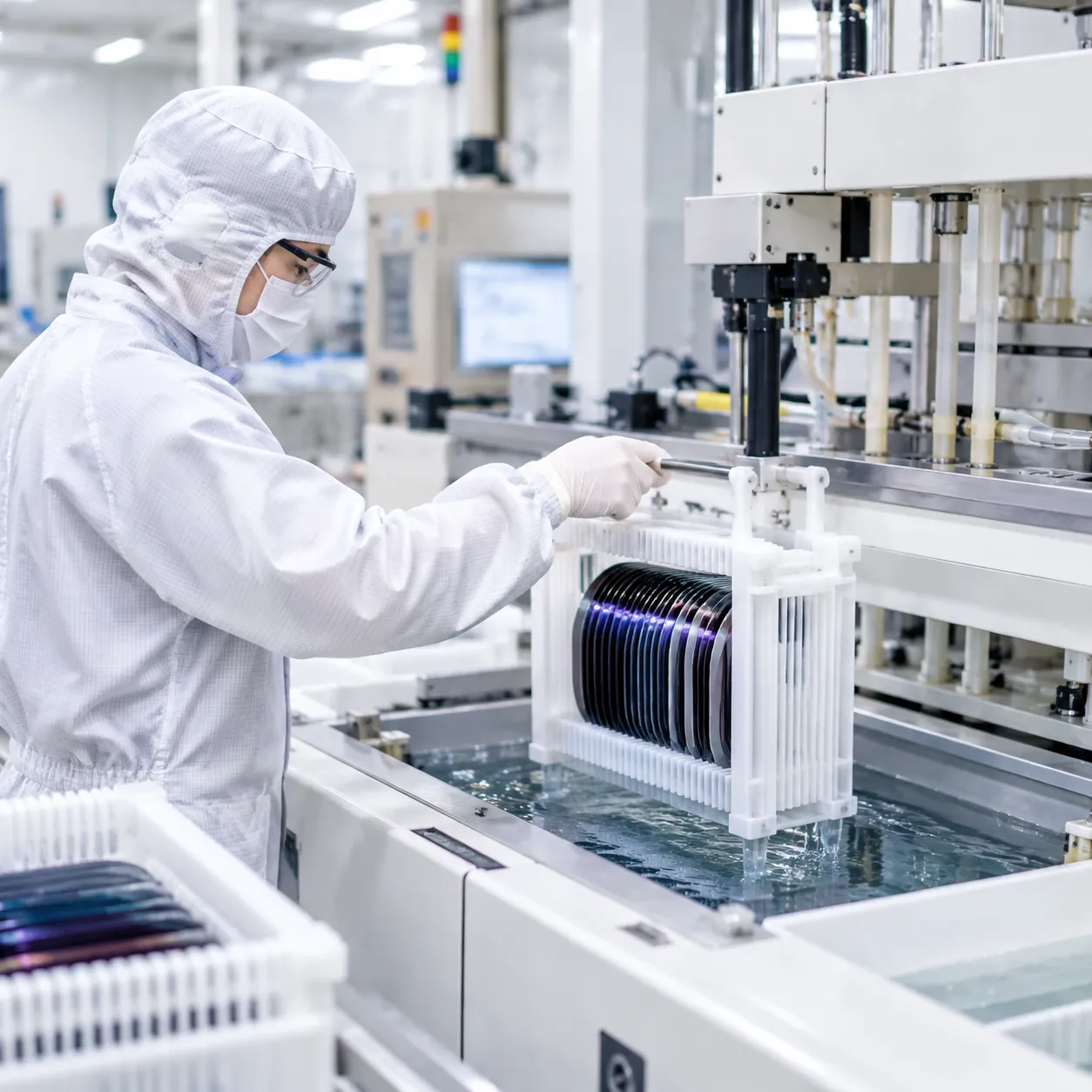
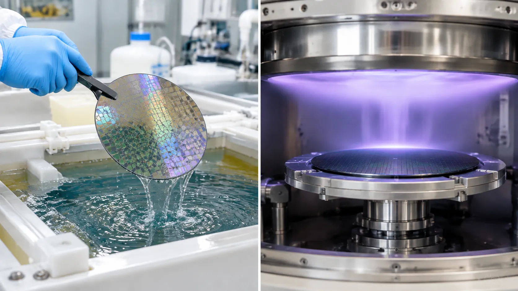
In our fab lines, stripping material predictably without blowing out critical dimensions or lifting resist masks comes down to mastering the wet bench. Chemical etching semiconductor substrates involves using liquid-phase chemical solutions to selectively strip away unprotected thin films or bulk crystalline layers. While plasma dry etching dominates sub-micron gate patterning, wet chemical etching remains our workhorse for wafer-level cleaning, pad oxide removal, isotropic recessing, and high-selectivity film stripping across high-volume wafer fabrication.
What Is Wet Chemical Etching in Semiconductor Fabrication?
Wet chemical etching relies on tailored liquid etchants—typically combinations of acids, bases, and strong oxidizers—to dissolve solid materials into soluble compounds. After completing the photolithography process, the patterned photoresist acts as a barrier, exposing only targeted regions of the wafer to the chemical bath.
We rely on wet etching primarily because of its undeniable operational strengths:
Exceptional etch rate selectivity: We can strip a top layer (such as silicon dioxide) at high speed while stopping dead on an underlying layer (such as silicon) with near-infinite selectivity ratios.
Low surface damage: Unlike plasma-based processes, wet chemistries avoid ion bombardment, preventing crystal lattice degradation, charge accumulation, and sub-surface crystal stress.
Massive batch throughput: Submerging cassettes of 25 to 50 wafers in a single tank delivers exceptional cost efficiency for non-critical dimensional targets.
The 3-Step Surface Reaction Mechanism
Every wet chemical etching cycle on a semiconductor substrate follows a fundamental three-step sequence at the liquid-solid boundary layer. Controlling this sequence determines whether an etch process yields uniform surfaces or runs into loading effects and rough topology.
-
- Diffusion of Reactants to the Wafer Surface
Active chemical species in the bulk solution travel through a stagnant fluid boundary layer toward the wafer face. Fluid agitation and bath circulation are critical here; without steady flow, local reactant starvation leads to uneven etch rates across the wafer diameter. - Surface Chemical Reaction
Once the etchant molecules reach the exposed substrate, they adsorb onto the surface. A chemical or oxidation-reduction reaction takes place: chemical bonds in the solid lattice break, and the target material converts into soluble byproducts or complex ions. - Diffusion of Reaction Byproducts into the Bulk Liquid
The dissolved byproducts desorb from the substrate and diffuse back out through the stagnant boundary layer into the main chemical bath. Efficient byproduct removal prevents local saturation, surface haze, and micro-masking defects.
- Diffusion of Reactants to the Wafer Surface
The overall etch speed is dictated by whichever step is slowest:
Reaction-rate limited regimes depend strictly on bath temperature and activation energy, producing highly uniform profiles across varying pattern densities.
Diffusion-limited regimes depend directly on chemical replenishment and fluid dynamics, making physical bath agitation and fluid delivery design essential for uniform profile control.
Wet Etching vs Dry Etching: Process Trade-Offs
Choosing between wet and dry processes in chemical etching semiconductor workflows comes down to balancing geometric precision with cost and speed. While reactive ion etching (RIE) dominates sub-micron pattern transfer, wet etching remains an indispensable workhorse across standard wafer fabrication lines. Understanding the fundamental wet etching vs dry etching semiconductor trade-offs helps us optimize operational budgets without compromising device yields.
Resolution, Cost, and Throughput Comparison
| Metric | Wet Chemical Etching | Dry Plasma Etching |
|---|---|---|
| Minimum Feature Size | Typically > 1 to 2 µm (limited by isotropic undercut) | Sub-10 nm capable (steep vertical profiles) |
| Capital & Running Cost | Low CAPEX; uses open or automated bath setups | High CAPEX; high vacuum and RF generators required |
| Etch Rate Selectivity | Extremely high (> 100:1 easily achieved) | Moderate to low (often 5:1 to 20:1) |
| Wafer Throughput | High (batch cassette immersion: 25–50 wafers/run) | Moderate to low (predominantly single-wafer chambers) |
| Substrate Surface Damage | Zero physical lattice damage; purely chemical | Potential ion bombardment damage and charging stress |
When to Choose Wet Chemical Etching Over Plasma
We consistently deploy wet chemical etching when process requirements shift away from vertical anisotropy toward high throughput, low thermal stress, and maximum material selectivity:
-
- Sacrificial Layer Stripping: Removing extensive layers of silicon dioxide or silicon nitride without removing a single nanometer of underlying silicon requires the superior etch rate selectivity that only wet baths deliver.
- Damage-Free Surface Cleans: Sensitive gate regions cannot tolerate the energetic ion bombardment or charge accumulation typical of plasma chambers. Wet chemistry eliminates lattice defects entirely.
- High-Volume Bulk Removal: For applications like wafer backside thinning, planar defect removal, and isotropic rounding of high-stress corners, immersion processing in a dedicated chemical wet bench for wafer cleaning and etching cuts processing cycle times significantly compared to dry vacuum systems.
- Broad-Feature Patterning: Non-critical layers in legacy nodes, power semiconductors, and MEMS architectures achieve lower cost-per-wafer targets using simple chemical baths instead of multimillion-dollar dry etch platforms.
Controlling Direction: Isotropic vs Anisotropic Chemical Etching Semiconductor Profiles
When we immerse patterned substrates into liquid etchants, the reaction profile dictates how closely the etched feature matches our mask. We split wet etch profiles into two distinct modes: isotropic (direction-independent) and anisotropic (orientation-dependent).
Isotropic Wet Etching and the Undercut Problem
Isotropic etching attacks the exposed film at equal rates in both vertical and lateral directions. While this uniform reaction works reliably for non-critical blanket strip steps and wafer cleaning, it creates severe geometry limits during fine-pitch patterning:
-
- Lateral Undercut: The etchant dissolves material directly beneath the resist edges at roughly the same rate it etches downward, creating a characteristic curved sidewall.
- Etch Bias and CD Loss: For every micrometer etched vertically into a target layer, the feature widens laterally by roughly the same depth per side, degrading target critical dimensions (CD).
- Mask Lifting: Excessive lateral undercut narrows the support surface under fine photoresist lines, causing mechanical collapse or mask peel-off during rinse cycles.
In our production lines, we minimize isotropic drift by shortening bath immersion times, optimizing agitations, and pairing processes with an engineered semiconductor wet etch process for wafer fabrication to lock down repeatable lateral etch rates.
Anisotropic Etching Along Silicon Crystal Planes
To avoid the undercut penalties of isotropic solutions on single-crystal silicon, we switch to crystallographic anisotropic wet etching. Alkaline solutions—such as potassium hydroxide (KOH) and tetramethylammonium hydroxide (TMAH)—etch single-crystal silicon at rates that vary sharply across different crystal planes.
-
- Atomic Packing Differences: Etch rates correlate directly with silicon surface atom density and back-bond counts. The loosely packed {100} and {110} planes expose vulnerable bonds and etch rapidly.
- The {111} Etch-Stop Barrier: The tightly packed {111} planes have three back-bonds anchored into the substrate, making their dissolution rate up to 100 to 400 times slower than {100} planes.
- Well-Defined Geometries: On standard (100) silicon wafers, anisotropic chemistries terminate cleanly against the {111} planes, generating stable, self-limiting V-shaped grooves with characteristic 54.74° sidewall angles. On (110) silicon, the same chemistry produces near-vertical trenches with parallel sidewalls.
| Profile Characteristic | Isotropic Wet Etch | Anisotropic Wet Etch |
|---|---|---|
| Primary Direction | Multidirectional (spherical front) | Crystallographically oriented |
| Typical Chemistries | HNA (HF + Nitric + Acetic), BOE | KOH, TMAH, EDP |
| Sidewall Geometry | Rounded, undercut profile | Predictable flat planes (e.g., 54.74°) |
| Primary Fab Role | Sacrificial layer removal, pad oxide etch | MEMS cavities, deep trenches, wafer texturing |
| Mask Tolerance | Requires intentional negative etch bias | Extremely tight pattern transfer to crystal planes |
Standard Chemical Formulations for Semiconductor Wafer Layers
Every layer on a processed wafer demands a distinct chemical formulation to achieve clean removal without destroying adjacent features. In our cleanroom operations, dialling in wet etch chemistries comes down to balancing etch rate, chemical selectivity, and bath stability. When running high-mix batches, we often deploy a standalone wet process bench for semiconductor labs to isolate aggressive acid baths and maintain pinpoint chemical bath control.
Silicon Substrate Etching with HNA and KOH
Silicon etching generally splits into isotropic and anisotropic chemistry based on whether crystal lattice selectivity is required:
-
- HNA (Hydrofluoric, Nitric, and Acetic Acid): This is our go-to isotropic mixture. Nitric acid oxidizes the raw silicon, hydrofluoric acid strips that newly formed oxide, and acetic acid acts as the buffer and diluent to keep the reaction front uniform across the wafer face.
- KOH (Potassium Hydroxide): A classic anisotropic wet etchant used heavily for bulk micromachining and MEMS. KOH attacks the silicon (100) and (110) planes rapidly while virtually stalling out on the densely packed (111) planes, forming sharp V-grooves and 54.74° sidewalls.
| Etchant System | Primary Target | Typical Selectivity | Common Process Temperature |
|---|---|---|---|
| HNA System | Bulk Si (Isotropic) | High over hard mask | 20°C – 25°C |
| KOH (20–40%) | Bulk Si (Anisotropic) | (100) vs (111) up to 400:1 | 70°C – 80°C |
| BOE (6:1 / 20:1) | Thermal / PECVD SiO2 | >100:1 over bare Si | Ambient (21°C – 23°C) |
| Hot H3PO4 (85%) | Silicon Nitride (Si3N4) | 30:1 to 50:1 over SiO2 | 150°C – 180°C |
Stripping Silicon Dioxide and Silicon Nitride Films
Dielectric layers require strict chemical selectivity to avoid punching through critical underlying gates:
-
- Silicon Dioxide (SiO2) Removal: Straight hydrofluoric acid (HF) works quickly, but for precise feature control, we run buffered oxide etch (BOE). BOE mixes HF with ammonium fluoride (NH4F) to buffer the solution, maintaining a steady pH and preventing rapid depletion that causes erratic etch rates.
- Silicon Nitride (Si3N4) Stripping: We use concentrated hot phosphoric acid (H3PO4) boiled at 160°C to 180°C. Reflux systems are mandatory here: if water evaporates from the bath, the acid concentrates, altering boiling points and degrading the oxide-to-nitride etch selectivity.
Chemical Solutions for Metal Interconnects and Wide-Bandgap Materials
Metallization layers and compound substrates require specialized chemical etching semiconductor solutions:
-
- Aluminum Lines: A standard PAN etch mixture (Phosphoric, Acetic, and Nitric acid heated to 40°C–50°C) strips aluminum interconnects smoothly without leaving residue strings.
- Copper and Barrier Layers: Dilute sulfuric acid with hydrogen peroxide (SPM variations) clears seed layers, while specialized fluorine-based solutions tackle titanium and tungsten barriers.
- Wide-Bandgap Substrates (SiC and GaN): Because silicon carbide and gallium nitride possess extreme chemical inertness, standard room-temperature wet chemistries fail. We turn to molten KOH at temperatures exceeding 450°C for defect revelation, or rely on photoelectrochemical (PEC) wet etching using UV-activated acid baths to achieve controlled dissolution.
Critical Control Parameters for Reliable Etch Rates
Balancing Bath Temperature, Chemistry, and Etch Selectivity
Etch rates follow Arrhenius kinetics—a temperature shift of just 1°C can alter reaction rates by up to 10% in aggressive acid mixtures. Tight process control demands continuous monitoring of both thermal profiles and chemical concentrations.
-
- Closed-Loop Thermal Management: We implement inline chemical heaters paired with dual-loop PFA heat exchangers to hold bath temperatures within ±0.5°C across the entire immersion vessel.
- Chemical Concentration Spiking: Evaporation and reactant consumption skew solution stoichiometry over time. For baths like BOE (Buffered Oxide Etch) or hot phosphoric acid, automated spiking replenishes volatile components to maintain steady etch rate selectivity between target films and underlying stop layers.
- Selectivity Window Tracking: High selectivity ensures the chemistry removes the exposed layer without pitting or eroding the underlying material. If the bath temperature climbs too high, selectivity against underlying barriers drops rapidly.
| Process Variable | Drift Impact | Target Control Window | Correction Method |
|---|---|---|---|
| Bath Temperature | Skewed etch depth, accelerated undercut | ±0.5°C | Recirculating heater / chiller with PID control |
| Active Chemical Concentration | Stalled etch rate, reduced selectivity | ±1.0 wt% | Automated chemical spiking and conductivity monitoring |
| Byproduct Saturation | Surface haze, premature reaction shutoff | Bath life limit (cassette count) | Timed tank drain, flush, and automated bath refresh |
Fluid Agitation, Bubble Clearance, and Etch-Stop Layers
Chemical reactions at the wafer surface generate microscopic boundary layers. Without continuous replenishment of fresh reactants, diffusion slows down, resulting in non-uniform etch profiles across wafer centers versus edges.
-
- Megasonic and Recirculation Agitation: Passive immersion leads to stagnant micro-environments inside deep trenches. We deploy low-velocity laminar flow recirculation combined with megasonic transducers to strip away depleted boundary layers without inducing photoresist pattern peel.
- Bubble Clearance Dynamics: Wet chemical etching reactions—particularly metal etching and silicon micromachining—frequently release hydrogen or oxygen gas microbubbles. Pinpinned bubbles act as micromasks, causing severe localized defects. Proper fluid flow sweeps these bubbles off the wafer pattern before they can adhere.
- Etch-Stop Layer Utilization: Etch-stop techniques provide the ultimate safety net against over-etching. Heavily boron-doped layers ($p^{++}$ silicon), buried thermal oxide (SOI structures), or silicon nitride films effectively halt the reaction when exposed, forgiving minor bath variations across the lot.
Integrating real-time sensor feedback through advanced automation control systems allows us to lock in fluid flow rates, track bath lifetime thresholds, and guarantee tight dimensional tolerances on every single run.
Step-by-Step Wet Etch Process Flow Integration
Integrating chemical etching into semiconductor wafer fabrication requires tight control from lithography prep to the final dry step. A single misstep during masking or rinsing ruins an entire lot through pattern lift-off or stain defects. Here is how we run this process cleanly on the floor.
Photoresist Mask Preparation and Priming
Before introducing aggressive chemical etchants, your mask needs flawless adhesion. Hydrophobic native surfaces or trapped moisture will cause immediate chemical seepage and lateral undercut.
-
- Dehydration Bake: We bake wafers at 150°C to drive off surface moisture before coating.
- HMDS Vapor Priming: We apply hexamethyldisilazane (HMDS) in a vapor prime oven to alter the substrate surface from hydrophilic to hydrophobic, establishing a strong bond with the photoresist.
- Hard Bake Optimization: After developing, a post-exposure hard bake (typically 110°C–130°C) cross-links the resist, boosting its chemical resistance against acidic baths like BOE or mixed acid solutions. Skipping this step leads directly to mask peeling and pattern loss.
Batch Immersion Tanks vs. Single-Wafer Spray Systems
Choosing how to expose the wafer to the chemistry depends entirely on your throughput targets, wafer diameter, and uniformity tolerances. We evaluate tools across two primary hardware formats:
| Process Factor | Batch Immersion Tanks | Single-Wafer Spray Systems |
|---|---|---|
| Throughput | High (25 to 50 wafers per carrier) | Low to Medium (wafer-by-wafer processing) |
| Etch Uniformity | Moderate (boundary layer variations) | Superior (continuous fresh chemical delivery) |
| Chemical Consumption | Lower cost per wafer via recirculating baths | Higher chemical consumption per run |
| Wafer Size Fit | Ideal for ≤200mm and legacy nodes | Preferred for 300mm advanced nodes |
For high-volume production where tool footprint and chemical cost dominate the equation, we utilize batch immersion wet bench systems for wafer processing. Conversely, when tight profile control on larger substrates is non-negotiable, moving to single-wafer wet processing equipment for 300mm fabs eliminates wafer-to-wafer cross-contamination and delivers fresh, uniform chemical distribution across the entire surface.
Quick-Dump Rinsing and Wafer Drying Techniques
Stopping a wet chemical etch accurately requires instant chemical displacement. Even a few extra seconds of residual acid exposure will alter feature critical dimensions (CD).
-
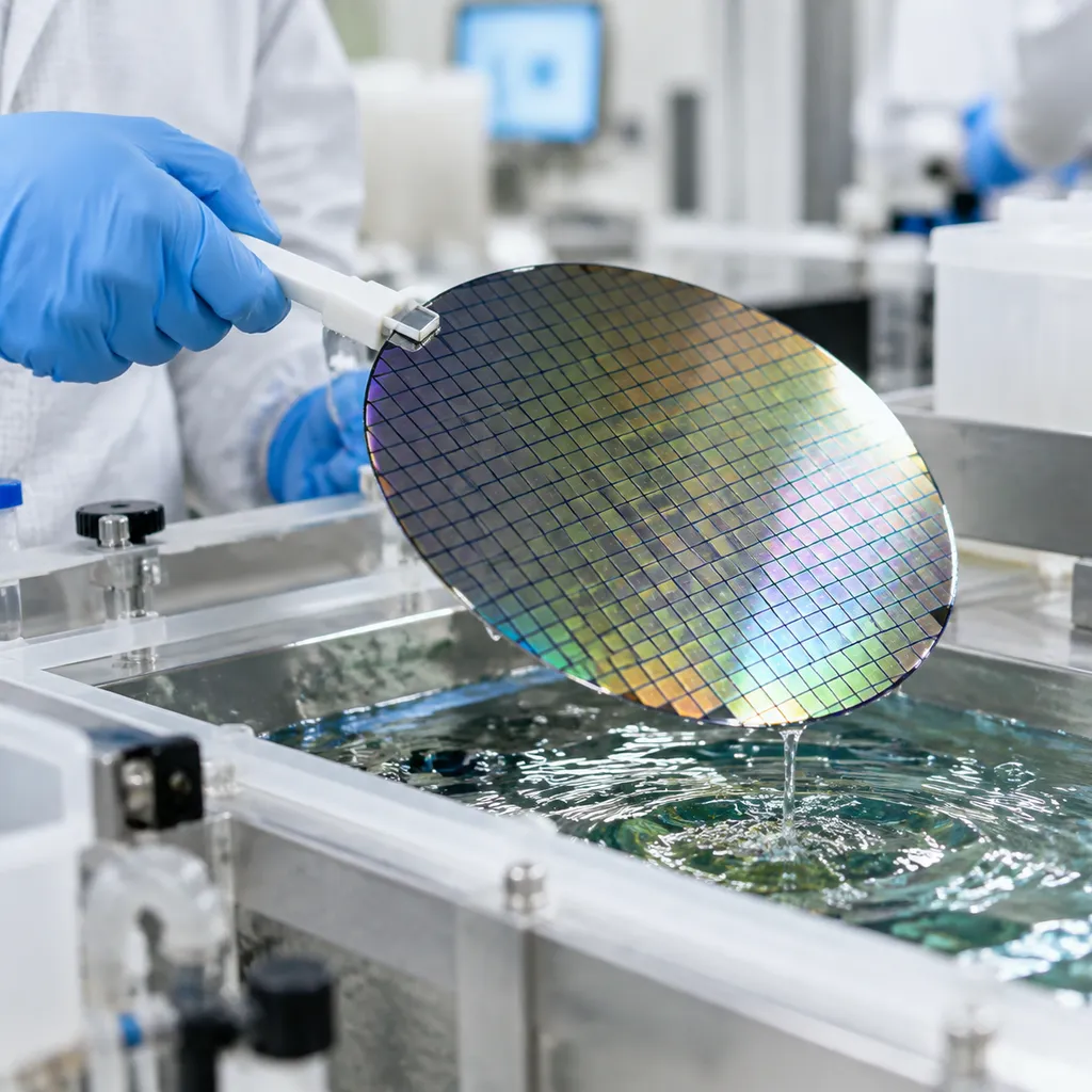
- Quick-Dump Rinsers (QDR): We immediately transfer etched wafers into a QDR tank. High-pressure deionized (DI) water fills the tank from the bottom, followed by a rapid bottom-valve release that dumps the volume in under five seconds. Repeating this cycle 3 to 5 times eliminates chemical carryover without allowing the wafers to dry in open air.
- Cascade Overflow Rinsing: Following the initial dump cycles, wafers sit in a continuous DI water overflow bath until resistivity reaches cleanroom baseline (typically >18 MΩ·cm), verifying total acid removal.
- Surface-Tension Drying (Marangoni / IPA Vapor): Standard spin-rinse dryers often leave water spots behind, especially on hydrophilic-hydrophobic patterned boundaries. We rely on Marangoni drying or isopropyl alcohol (IPA) vapor drying. The surface tension gradient pulls moisture cleanly off the wafer face, delivering a spot-free, defect-free semiconductor substrate clean ready for downstream metrology.
Troubleshooting Common Chemical Etching Defects
Preventing Lateral Undercut and Resist Peeling
Excessive lateral etch attack ruins critical dimension (CD) budgets and lifts photoresist masks off the substrate. We tackle these peel and undercut issues with specific pre-treatment and bath controls:
-
- Enforce HMDS Priming: Hydrophobic substrate prep is non-negotiable. Vapor-phase HMDS (hexamethyldisilazane) applied at 150°C ensures the resist adheres under acidic strain.
- Optimize Hard Bake Profiles: Under-baking leaves residual solvents that invite acid penetration along the interface. We ramp hard bakes to 120°C–130°C to cross-link the resist boundary without cracking the polymer.
- Switch to Buffered Chemistries: Unbuffered acids attack aggressively in all directions. Shifting to buffered oxide etchants (BOE) stabilizes hydronium ion concentration, reducing lateral bias while preserving etch rate selectivity.
- Implement Tight Chemical Process Management: Spikes in bath temperature accelerate lateral mass transport faster than vertical etching. Automated chemical spiking and constant bath circulation suppress wild CD deviations across 200mm and 300mm wafer fabrication lines.
Fixing Surface Haze, Micromasking, and Incomplete Removal
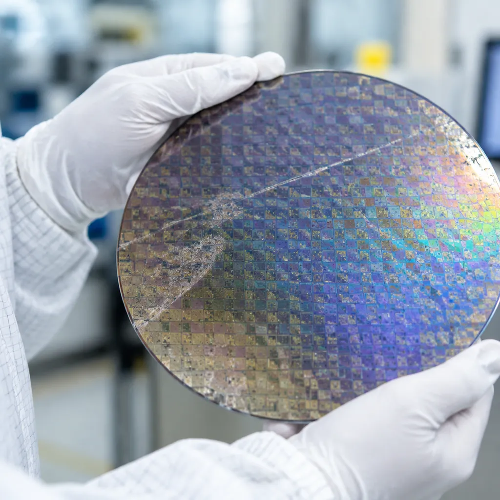
Surface haze and residual pillars typically stem from insoluble reaction byproducts or trapped microbubbles shielding the surface.
| Etch Defect | Root Cause | Cleanroom Solution |
|---|---|---|
| Micromasking ("Grass") | Sputtered resist flakes or insoluble precipitates | Add megasonic agitation to displace boundary precipitates; filter recirculation loop at 0.05 µm. |
| Surface Haze | Non-uniform native oxide regeneration or bath saturation | Run an immediate diluted acid rinse; dump bath before chemical loading exceeds saturation thresholds. |
| Incomplete Removal | Hydrogen bubble entrapment blocking mass transport | Lower chemical surface tension using fluorosurfactants; adjust cassette agitation frequency. |
| Residue / Staining | Slow deionized water displacement after bath pull | Transition to high-flow quick-dump rinsing (QDR) and IPA vapor drying immediately after etch. |
If surface contaminants or organic residues persist prior to chemical exposure, a pre-etch semiconductor substrate clean using fresh Piranha solution (SPM) eliminates organic micro-masks, ensuring uniform chemical contact across every die.
Cleanroom Safety and Acid Waste Management in Chemical Etching

Handling Hydrofluoric Acid and Essential Safety Gear
A hydrofluoric acid etch is uniquely hazardous because fluoride ions penetrate deep into soft tissue and attack bone structures without causing immediate surface burns. When running oxide removal baths, our operators rely on dedicated PPE and engineering controls:
-
- Chemical PPE Stack: We enforce heavyweight neoprene or butyl gloves over nitrile under-gloves, full-face chemical shields over safety glasses, and chemical aprons impervious to fluorides.
- Emergency Chemistry: Tubes of calcium gluconate gel (2.5%) sit within arm's reach of every etch bath to bind free fluoride ions immediately in the event of accidental skin contact.
- Containment Hardware: Manual and automated chemical transfers must happen inside a dedicated acid wet bench for safe chemical processing, equipped with lip exhausts that maintain an inward face velocity between 100 and 120 FPM (feet per minute) to prevent fumes from breaking into the cleanroom aisle.
| Hazard Factor | Process Chemical | Primary Personal Risk | Dedicated Control Measure |
|---|---|---|---|
| Dermal / Systemic | Hydrofluoric Acid (HF, BOE) | Hypocalcemia, deep tissue necrosis | Calcium gluconate, butyl gloves, automated bath covers |
| Vapor / Respiratory | Hot Nitric / Hydrochloric Acid | Pulmonary edema, mucosal burns | Push-pull deck ventilation, continuous flow sensors |
| Exothermic Reaction | Piranha Clean (SPM) | Thermal burns, explosive outgassing | Temperature-controlled quartz tanks, slow H₂O₂ dosing |
Neutralizing Acid Exhaust and Treating Fluoride Waste
Managing wet chemistry does not end when the wafer moves to the rinse tank. Exhaust streams and spent chemical baths must be separated at the point of origin:
-
- Point-of-Use Exhaust Scrubbing: Acid fumes pulled from bench plenum lines route directly into multi-stage acid gas scrubbers, which use packed-bed towers with recirculating alkaline solutions (typically sodium hydroxide) to neutralize acid vapors before atmospheric release.
- Segregated Drain Plumbing: We separate drain networks into acid waste neutralization (AWN) streams for general acids and a segregated concentrated fluoride drain for spent HF and BOE baths.
- Fluoride Precipitation: Standard AWN systems cannot discharge fluoride safely because local wastewater limits often cap fluoride at under 10–20 ppm. We treat fluoride waste by precipitating it out with hydrated lime (calcium hydroxide) or calcium chloride ($CaCl_2$), forming insoluble calcium fluoride ($CaF_2$) cake that can be filtered, dewatered, and safely hauled off-site.
Next-Gen Uses for Precision Chemical Etching
As critical dimensions shrink and packaging gets tighter, dry plasma etching cannot handle every high-aspect or damage-sensitive step alone. In our cleanroom lines, advanced chemical etching semiconductor processes solve the physical limits of dry tools—delivering damage-free lattice surfaces, omnidirectional clearing, and atomic-scale material selectivity.
| Next-Gen Application | Target Layer / Structure | Chemistry Mechanism | Core Advantage |
|---|---|---|---|
| MEMS Micromachining | Bulk Si, Oxide hard masks | Anisotropic crystallographic etching (KOH/TMAH) | Ultra-smooth sidewalls without plasma damage |
| Wafer Thinning | Backside bulk Silicon | Controlled acid spin-etch (HF/HNO3/H3PO4) | Relieves grinding stress; prevents die warpage |
| GAA Nanosheet Release | Sacrificial SiGe layers | High-selectivity redox chemistry | Zero damage to suspended Silicon channels |
Micromachining MEMS and High-Aspect Features
In MEMS processing, plasma tools can cause surface micro-roughness and charge buildup that ruin sensitive inertial sensors, pressure diaphragms, and microfluidic channels. We use anisotropic wet chemical etching to carve precise geometries dictated by crystal planes rather than lithography tool limits:
-
- Cavity and diaphragm release: Deep etching stops abruptly on silicon (111) planes, forming exact 54.74° sidewalls with mirror finishes.
- Zero residual stress: Wet etchants leave underlying mechanical layers free of the ion bombardment damage typical of dry tools.
- Uniform undercutting: Cantilevers and suspended comb drives clear completely without stiction or mechanical breakage.
Stress-Relief Wafer Thinning in Advanced Packaging
Mechanical backgrinding thins wafers down to 30–50 µm for high-density 3D stacking, but it leaves deep micro-cracks and crystalline lattice defects on the backside. If left untreated, these defects cause wafer warpage, die cracking, and catastrophic thermal failures during thermocompression bonding.
Using optimized chemical mixtures on our high-precision wet benches for semiconductor processing, we strip away the damaged 2 to 5 µm silicon fracture zone. This acid-based spin-etch smoothens surface topography, removes stress concentrators, and restores wafer fracture strength—making it an essential preparation step for advanced semiconductor packaging architectures like chiplets and heterogeneous 2.5D/3D-IC integrations.
Selective Sacrificial Etching in Gate-All-Around (GAA) Architectures
Sub-3nm logic nodes rely on Gate-All-Around (GAA) nanosheet transistors, where the critical milestone is suspending multi-tier horizontal silicon channels. The manufacturing challenge requires stripping alternating silicon-germanium (SiGe) sacrificial layers out from between ultra-thin pure silicon channels:
-
- Near-infinite selectivity: We deploy tailored wet chemical solutions that dissolve SiGe while maintaining a selectivity ratio greater than 150:1 against pure Si.
- Capillary defect prevention: Precise chemical surface-tension balancing prevents liquid capillary collapse from snapping suspended silicon channels together during release.
- Pristine interfaces: Wet solutions clear nanometer-wide channels completely without physical ion collision, delivering clean interfaces ready for atomic layer deposition (ALD) high-k metal gate stacks.
Frequently Asked Questions About Semiconductor Chemical Etching
In our daily wafer fabrication routines, we run into recurring process integration challenges with wet chemistry. Here are straightforward answers to the common questions engineers and technicians ask on the fab floor regarding wet chemical etching.
What is the difference between BOE and straight HF?
Straight hydrofluoric acid (HF) rapidly depletes its active fluoride ions during silicon dioxide removal. This depletion causes the etch rate to drop quickly, leading to process drift and non-uniform film removal across the wafer batch.
Buffered Oxide Etch (BOE) blends straight HF with a buffering agent, typically ammonium fluoride (NH4F), usually in volume ratios like 6:1 or 10:1.
-
- Stable pH and Etch Rate: The ammonium fluoride continuously replenishes fluoride ions consumed during oxide dissolution, maintaining a flat, predictable etch rate throughout the bath's lifetime.
- Photoresist Protection: Straight HF aggressively attacks and degrades photoresist adhesion. BOE stabilizes bath pH, minimizing resist peel and lateral undercut.
- Controlled Selectivity: We rely on BOE when precision pattern transfer on thermal oxide or LPCVD oxide is required without losing critical dimension control.
| Parameter | Straight HF | Buffered Oxide Etch (BOE) |
|---|---|---|
| Primary Composition | HF diluted in DI water (e.g., 49% or 1:50) | NH4F + HF (e.g., 6:1 volume ratio) |
| Bath Life Stability | Degrades quickly as HF is consumed | High; buffered pH maintains constant etch rate |
| Resist Compatibility | Poor; causes early lift-off and pinholes | Superior; gentle on standard photoresist masks |
| Typical Fab Task | Fast native oxide dips, pre-diffusion cleans | Patterned SiO2 etching with photoresist masks |
Why does anisotropic wet etching stop on the (111) plane?
When running anisotropic wet etching with potassium hydroxide (KOH) or TMAH on silicon substrates, chemical attack rates depend heavily on crystallographic orientation. The etch rate on the (100) plane is roughly 100 to 400 times faster than on the (111) plane.
-
- Atomic Density: The (111) crystal plane features the highest packing density of silicon atoms.
- Dangling Bonds: Atoms on the (111) plane expose only a single back-bond to the surface, whereas (100) atoms expose two dangling bonds.
- Steric Hindrance: Hydroxide ions (OH-) face significant steric shielding when trying to insert into the tightly packed back-bonds of the (111) lattice.
Because the activation energy required to break these bonds on the (111) surface is significantly higher, chemical etching essentially arrests when it encounters this plane. This crystallographic halt enables us to produce predictable, self-terminating V-grooves and 54.74-degree sidewalls in bulk micromachining.
How do we stop photoresist lift-off during long acid etches?
Photoresist delamination usually stems from poor surface prep, excessive surface moisture, or stress at the mask-to-substrate boundary. To maintain resist adhesion during demanding chemical etching runs, we follow these practices:
-
- Dehydration Bakes and HMDS Priming: Never skip the dehydration bake. Dehydrate wafers at 150°C to 200°C, then immediately apply hexamethyldisilazane (HMDS) in a vapor prime oven to replace surface hydroxyl groups with hydrophobic methyl groups.
- Aggressive Hard Bakes: Step up the post-exposure hard bake temperature (typically 120°C to 130°C for positive resists) to cross-link the resist matrix and drive off residual casting solvents before tank immersion.
- Surfactant Dosing: Add a small amount of non-ionic fluorosurfactant to the chemical etch bath. Lowering surface tension promotes gentle surface wetting and prevents etchant from penetrating micro-voids beneath the resist edges.
- Use Automated Chemical Handling: Mechanical stress from manual wafer dipping can peel compromised resist edges. We integrate recipes inside automated wet station semiconductor equipment for wafer processing to guarantee smooth liquid handling, controlled fluid turbulence, and uniform boundary layer dynamics.
Is wet chemical etching suitable for sub-micron nodes?
For primary front-end pattern transfer, standard isotropic wet etching is rarely used at sub-micron dimensions below 0.25 µm. Because isotropic chemistries etch laterally under the resist mask at the same rate they etch downward, undercut destroys critical dimension (CD) tolerances at nanoscale pitches.
However, wet chemical processing remains indispensable at advanced nodes (including 7nm, 5nm, and GAA architectures) for specific, highly selective operations:
-
- Sacrificial Layer Stripping: Removing SiGe sacrificial nanosheets in Gate-All-Around (GAA) architectures without attacking adjacent silicon channels.
- Selective Nitride Pullback: Hot phosphoric acid stripping of Si3N4 hardmasks with ultra-high selectivity to silicon dioxide and bulk silicon.
- Surface Cleaning and Native Oxide Clears: Dilute HF cleans prior to atomic layer deposition (ALD) and epitaxy to secure atomically pristine surfaces without causing plasma-induced lattice damage.