Formula details
Product Details
Overview
Comprehensive Contamination Control for Advanced Substrate Preparation
Core Surface Contamination Mechanisms
Modern fab lines face four primary contamination vectors that directly impact device performance and dielectric breakdown:
-
- Sub-micron Particulates: Slurry residues, silica particles, and environmental dust adhering via van der Waals and electrostatic forces.
- Native & Chemical Oxides: Non-uniform, uncontrolled oxide layers (10–20 Å) that impede epitaxial growth, alter contact resistance, and trap impurities.
- Trace Metallic Ions: Mobile ions (Fe, Cu, Ni, Zn) causing junction leakage, reduced carrier lifetime, and gate dielectric degradation.
- Organic Adsorbents & Carbon Films: Airborne molecular contamination (AMCs), residual photoresists, and solvent traces creating hydrophobic patches that disrupt uniform etching.
Cleaning Stages Across the Substrate Lifecycle
Our silicon wafer cleaning equipment delivers target cleanliness metrics across all critical substrate fabrication checkpoints:
-
- Prime Wafer Slicing & Lapping: Coarse particle degreasing, wire-saw slurry stripping, and mechanical damage layer removal.
- Pre-Epitaxy (Pre-Epi): Hydrophobic oxide-free surfaces with zero organic carbon residue, ready for atomic-level lattice alignment.
- Post-Chemical Mechanical Planarization (Post-CMP): Rapid slurry particle detackification, chemical brush scrubbing, and metal ion chelation without surface scratching.
- Front-End-of-Line (FEOL) Cleans: Ultra-clean interfaces prior to gate oxidation, diffusion, and high-k dielectric deposition where particle limits reach single-digit counts at sub-20nm nodes.
Platform Architectures: Immersion vs. Single-Wafer vs. Scrubbing
Selecting the appropriate processing architecture depends on wafer throughput requirements, defect budgets, and cross-contamination limits:
| Platform Architecture | Dominant Clean Mechanism | Typical Throughput | Ideal Fab Integration |
|---|---|---|---|
| Batch Wet Immersion Benches | Multi-tank chemical immersion with overflow rinses | Up to 500 wafers/hour | Bulk stripping, native oxide removal, prime wafer manufacturing |
| Single-Wafer Spin Processors | Dual-fluid spray, single-side chemical dispensing, megasonics | 30 to 60 wafers/hour | FEOL critical gate cleans, low cross-run contamination, high warpage substrates |
| Mechanical Wafer Scrubbers | Dual-sided PVA roller brushes with micro-jet fluidics | 45 to 80 wafers/hour | Post-CMP planarization, macroscopic slurry debonding, bevel edge cleaning |
We engineer each platform to minimize chemical carryover, eliminate watermark signatures, and guarantee uniform particle removal efficiency (PRE) across 100mm to 300mm substrate footprints.
Integrated Chemical and Physical Cleaning Technologies
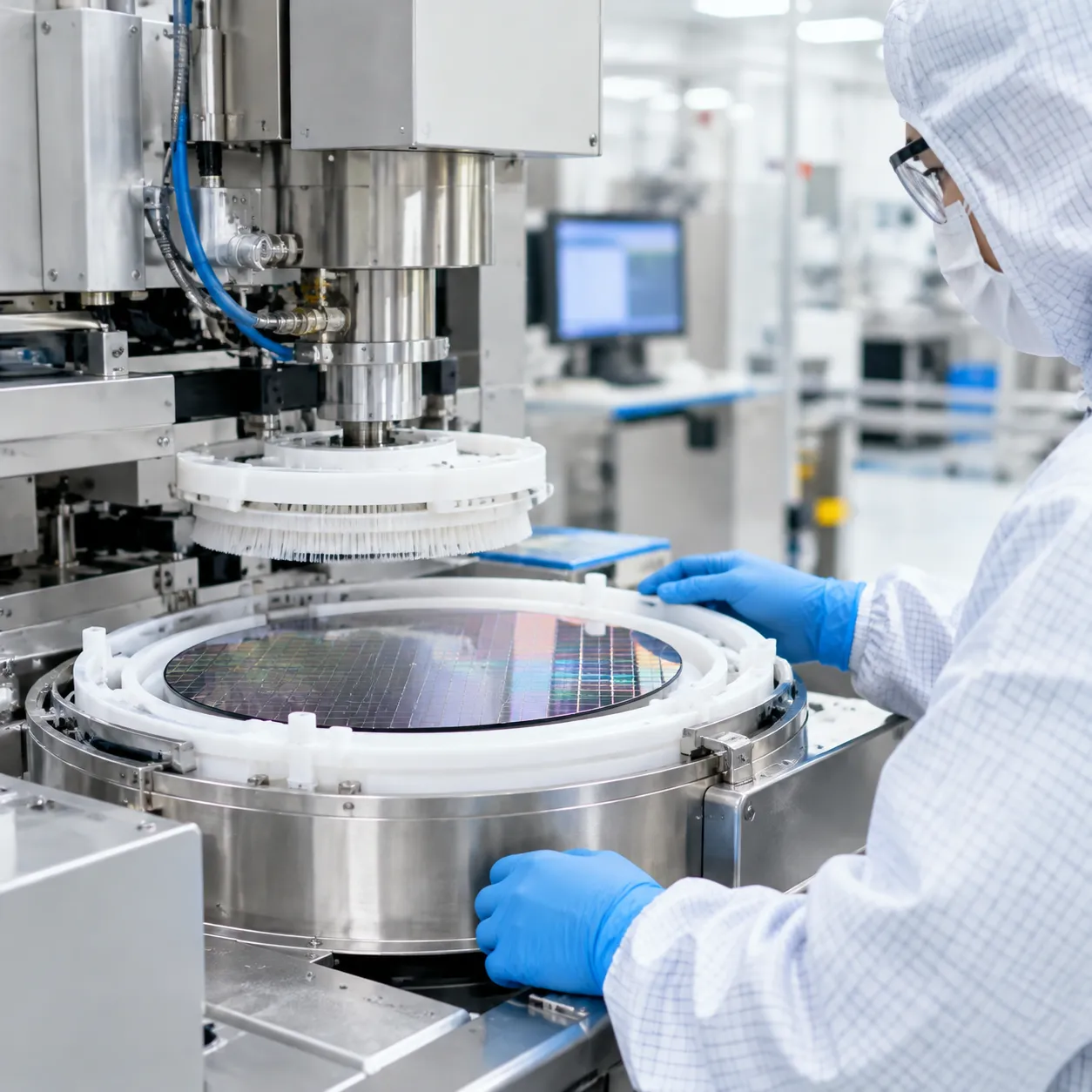
To reach ultra-low defect densities, our silicon wafer cleaning equipment blends targeted wet chemical baths with active physical dislodgement mechanisms.
Standard Chemical Sequences and Oxide Removal
We configure our chemical delivery loops to support standard RCA recipes alongside aggressive etching solutions:
-
- SC-1 (Standard Clean 1): Ammonium hydroxide, hydrogen peroxide, and DI water (NH₄OH/H₂O₂/H₂O) at 70°C–80°C. Delivers controlled surface undercutting to release sub-micron particles and strip light organic residues.
- SC-2 (Standard Clean 2): Hydrochloric acid, hydrogen peroxide, and DI water (HCl/H₂O₂/H₂O) at 70°C–80°C. Promotes soluble complex formation for rapid metallic ion desorption.
- SPM (Piranha Clean): High-temperature sulfuric acid and hydrogen peroxide (H₂SO₄/H₂O₂) to oxidize stubborn cross-linked photoresist and heavy organic residues.
- DHF / BOE Baths: Diluted hydrofluoric acid (DHF, 0.5%–2%) and buffered oxide etchants (BOE) to etch thermal and native oxides, producing uniform, hydrogen-passivated hydrophobic silicon surfaces.
We engineer these sequences directly into our modular chemical wet bench for wafer cleaning and etching setups, ensuring closed-loop temperature control and dynamic chemical spiking.
Physical Scrubbing and Megasonic Field Delivery
Fine particle removal on advanced substrates requires kinetic energy tuned below the structural damage threshold:
-
- Multi-Frequency Megasonics (800 kHz to 2 MHz): Piezoelectric transducer arrays create controlled acoustic cavitation and acoustic streaming. Operating above 800 kHz thins the fluid boundary layer, dislodging sub-50nm particles while protecting high-aspect-ratio patterns from cavitation pit damage.
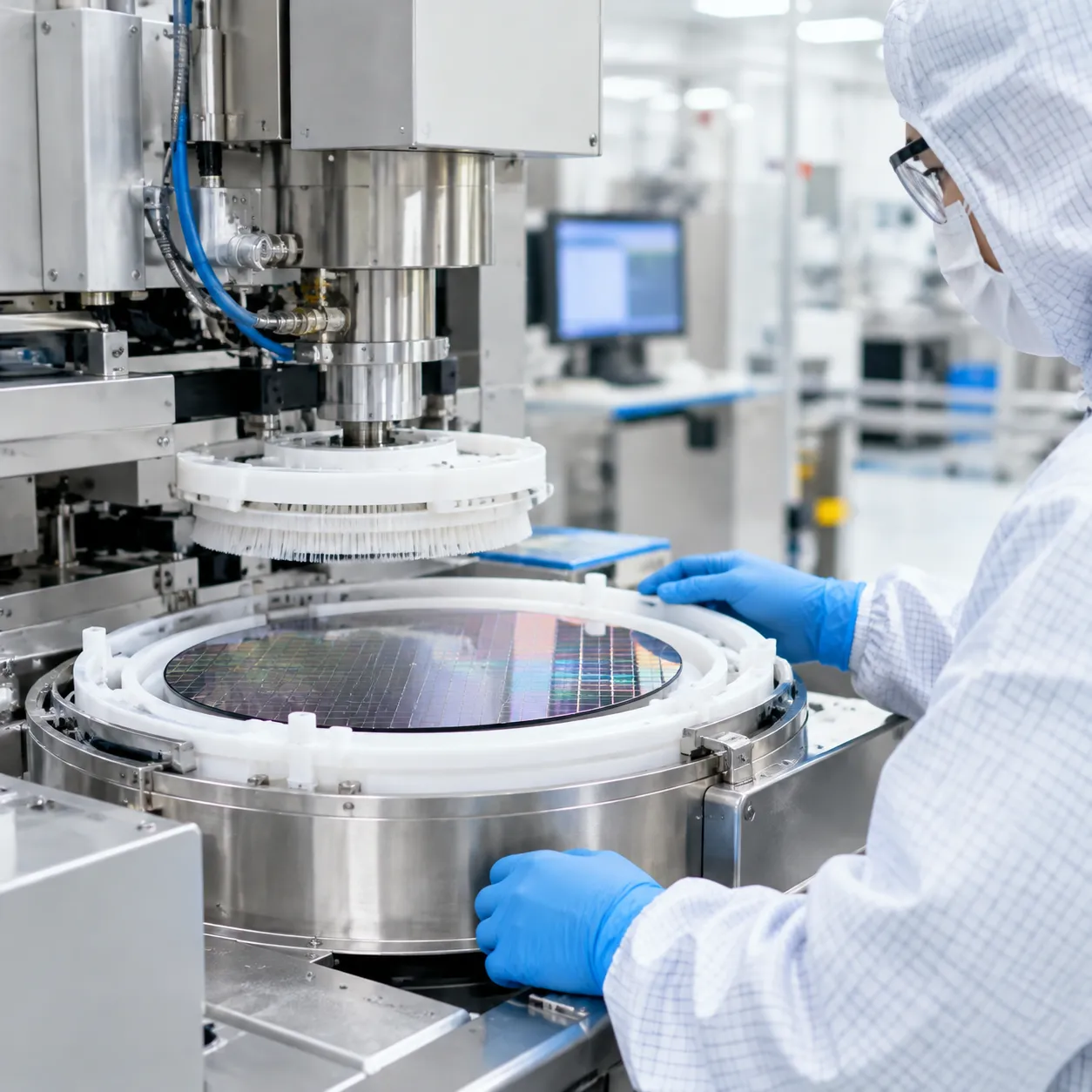
- Dual-Sided PVA Roller Brushes: Soft polyvinyl alcohol (PVA) brushes contact both sides of the wafer simultaneously with continuous fluid delivery, mechanically breaking up slurry cakes and silica residues post-CMP.
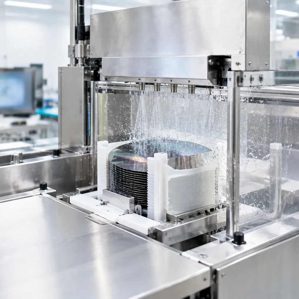
- High-Pressure Micro-Jet Fluidics: Fan nozzles sweep atomized DI water across the wafer surface at regulated pressures to flush dislodged particulates toward peripheral drain channels.
Advanced Surface Drying Systems
Drying represents the most critical step in equipment for silicon wafer substrate preparation cleaning to prevent pattern collapse and watermark defects.
| Drying Technology | Mechanism | Target Application | Defect Prevention |
|---|---|---|---|
| Marangoni Surface Tension | Alcohol gradient lowering surface tension at the meniscus | Hydrophobic surfaces with exposed Si/Poly-Si | Eliminates watermark deposition |
| Heated IPA Vapor | Controlled condensation and displacement | High-aspect-ratio trench architectures | Prevents capillary pattern collapse |
| Filtered N₂ Knife | Low-angle, high-velocity ionized nitrogen boundary | Planar wafer geometries and high-throughput lines | Zero residual trace moisture |
Technical Specifications of Silicon Wafer Cleaning Equipment
Core Engineering Parameters
| Parameter | Batch Immersion Systems | Single-Wafer Processors |
|---|---|---|
| Wafer Sizes Supported | 100mm, 150mm, 200mm, 300mm | 150mm, 200mm, 300mm |
| Throughput Capacity | Up to 50 wafers/run (dual cassette) | 35 to 60 wafers/hour per chamber |
| Wetted Tank Materials | Fused quartz, high-purity PFA, PTFE, PVDF | Solid PTFE chamber, PFA fluid lines |
| Filtration Rating | Point-of-use (POU) down to 0.02 µm | Fresh chemistry dispense / 0.05 µm POU |
| Thermal Range & Stability | Ambient to 180°C (±0.5°C via closed-loop PID) | 20°C to 80°C dispense control |
| Recirculation Rates | 15 to 40 L/min with magnetic-drive pumps | Continuous single-pass or recirculated sump |
Choosing between high-volume tank systems and dedicated single-substrate stations depends directly on your line throughput and chemical sensitivity. For a detailed breakdown of tool selection criteria, see our guide on batch immersion vs. single-wafer wet processing.
Substrate Handling and Chemical Control
Our silicon wafer cleaning equipment integrates high-precision fluid dynamics and hardware protection to maximize bath life and yield:
-
- Substrate Flexibility: Configured for standard prime wafers, thin substrates down to 100 µm, and reclaimed carrier discs across 100mm, 150mm, 200mm, and 300mm form factors.
- Corrosion-Resistant Fluid Paths: All chemical manifolds, tanks, and valves use ultra-pure PTFE and PFA to eliminate trace metal leaching in SC-1, SC-2, and SPM operations.
- Active Bath Filtration: Continuous point-of-use (POU) loops run seal-less, magnetically driven fluoropolymer pumps to maintain uniform bath agitation without mechanical particle shedding.
- Closed-Loop Thermal Management: Inline quartz heaters and external heating jackets use dual-sensor PID loops, preventing thermal overshoot and keeping chemical activity steady over long shift cycles.
- Chemical Consumption Reduction: Dynamic bath spiking and automated concentration controls extend bath usage intervals, cutting total chemical draw and waste treatment volume by up to 30%.
Industrial Fab Automation, Transfer Robotics, and Safety
Modern fab yield hinges on eliminating manual handling variability and maintaining tight bath control. We engineer our silicon wafer cleaning equipment with end-to-end automation, real-time chemical metrology, and certified cleanroom safety architectures to ensure zero-defect transfers and uncompromised operator safety.
Precision Robotic Substrate Handling
To avoid backside damage and surface micro-scratches during high-speed chemical immersion, we integrate specialized cleanroom transfer robotics designed for thin and prime substrates alike:
-
- Non-Contact Bernoulli Chucks: Utilize air cushions to support fragile or warped substrates with zero frontside surface contact.
- Precision Edge-Grip End-Effectors: Clamp strictly within the wafer exclusion zone (<2 mm) using chemical-resistant PEEK or PTFE contact pads.
- Multi-Axis Servo Actuators: Deliver smooth, vibration-free acceleration and deceleration profiles across acid, etch, and rinse stations.
Factory MES Integration and Real-Time Analytics
Our automated systems connect directly with your fab host to maintain tight process windows and batch-to-batch repeatability:
-
- SECS/GEM Protocols (SEMI E30, E37): Standard HSMS Ethernet communication ensures seamless tracking of wafer lots, dynamic recipe selection, and real-time alarm reporting.
- Real-Time Spiked Dosing: Automatic replenishment systems calculate chemical consumption rates and inject micro-doses of chemistry (such as H2O2, NH4OH, or HCl) to keep bath concentrations stable without dropping bath volume.
- Inline NIR Spectroscopy & Conductivity Metrology: Near-infrared chemical analyzers continuously measure active acid, base, and oxidizer concentrations, preventing process drifts before they impact yield.
| Automation & Control Feature | Engineering Implementation | Fab Process Advantage |
|---|---|---|
| Robotic End-Effector | PEEK edge-clamp / Bernoulli chuck | Zero active-area contact; handles thinned wafers |
| Host Interface | SECS/GEM (E30, E37 HSMS) | Automated lot tracking and recipe execution |
| Inline Bath Metrology | NIR spectroscopy & conductivity loops | Extends bath life and prevents bath depletion |
| Cleanroom Isolation | Mini-environment with dedicated fan filter units | Direct ISO Class 1 compatibility at the chuck interface |
Safety Compliance and Cleanroom Reliability
Designing reliable equipment for silicon wafer substrate preparation cleaning requires rigorous fire, chemical, and environmental containment. We build each automated line to comply fully with SEMI S2 and SEMI S8 standards. For hazardous chemistry zones, our tools feature FM4910-compliant flame-retardant materials, continuous exhaust airflow interlocks, dual-containment fluid tubing, and integrated CO2 or clean-agent fire suppression. Integrating these systems into a dedicated semiconductor wet bench cleanroom for precision cleaning delivers true ISO Class 1 to Class 3 local cleanliness while isolating operators from aggressive chemical vapor pathways.
Process Applications Across Device Fabrication Modules
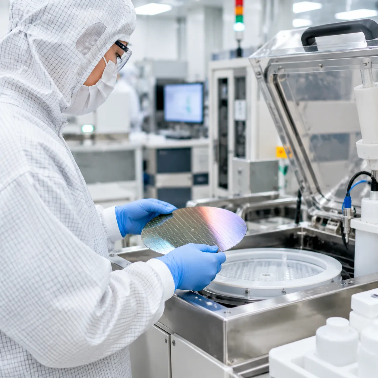
| Fabrication Stage | Target Contaminants | Core Process Module | Cleaning Mechanism |
|---|---|---|---|
| Prime Wafer Prep | Wire-saw slurry, abrasives, cutting oils | High-throughput batch wet bench | Surfactant wash, megasonic degrease, chemical etch |
| FEOL Pre-Gate | Native oxides, trace metallic ions (Fe, Cu, Ni) | Multi-tank RCA station / Single-wafer chamber | SPM, DHF oxide strip, dilute SC-1/SC-2 chemistry |
| Post-CMP | Slurry nanoparticles (silica, ceria), organics | Dual-sided PVA brush wafer scrubber | Mechanical scrub with alkaline/acidic chemistry |
| 3D Packaging | Debond adhesive residue, polymer buildup | Specialized spin processor | Controlled organic solvent rinse with N2 drying |
Prime Wafer Production: Post-Wire-Saw Slurry Stripping and Chemical Polishing Deglaze
Raw substrate slicing introduces aggressive particulate loads that must be cleared before downstream thermal steps:
-
- Slurry Stripping: We clear dense diamond suspension residues, silicon kerf dust, and organic carrier fluids using concentrated alkaline soaks combined with directional megasonic energy.
- Chemical Polishing Deglaze: Following chemical-mechanical or acid polishing, our immersion baths deliver uniform oxide etching and surface planarization, stabilizing the wafer prior to epitaxial growth.
- Surface Activation: Controlled chemical oxide regrowth preps virgin substrates for consistent baseline resistance across the entire batch.
Front-End-of-Line (FEOL): Pre-Gate Oxidation and Implant Residue Removal
FEOL demands our highest purity envelope. When preparing critical silicon interfaces, our equipment for silicon wafer substrate preparation cleaning provides atomically clean surfaces without damaging sub-micron geometries. For detailed integration blueprints, explore our wafer cleaning systems guide.
-
- Pre-Gate Oxidation Cleaning: Complete desorption of trace mobile ions and metallic species down to undetectable limits (< 1E9 atoms/cm²) using optimized SC-1 and SC-2 sequences.
- Native Oxide Etching: Rapid DHF or buffered oxide etch (BOE) modules strip native SiO2 layers with nanometer-level etch uniformity.
- Post-Ion Implant Clean: We deploy advanced chemical mixtures to strip heavily crust-hardened photoresists and residual polymers without pitting the exposed active regions.
Post-CMP Clean: Slurry Removal Without Metallic Cross-Contamination
Chemical Mechanical Planarization leaves stubborn nanoparticles and organic stabilizers that quickly bind to dielectric and barrier layers. We tackle this by pairing physical and chemical mechanisms inside dedicated chambers:
-
- Non-Contact and Contact Scrubbing: Dual-axis PVA roller brushes deliver synchronized, non-destructive mechanical force directly to both wafer faces.
- Nanoparticle Release: Dilute ammonium hydroxide or organic acid chemistries alter the wafer and particle zeta potentials, repelling nanoparticles from the surface to prevent redeposition.
- Cross-Contamination Safeguards: Dedicated fluid isolation shields copper, tungsten, and dielectric modules, eliminating metal carryover between successive runs in our single-wafer wet clean system for precision cleaning.
Advanced Packaging and 3D Integration: Thin Wafer Handling and Compound-on-Si
Modern packaging architectures introduce mechanical fragility and thermal sensitivity that standard processing tools cannot accommodate:
-
- Taiko and Ultra-Thin Wafers: We process substrates thinned down to <50 µm using non-contact Bernoulli chucks and edge-grip clamping to eliminate backside mechanical stress and prevent edge chipping.
- Temporary Carrier Debond Cleaning: Efficient solvent-based single-wafer processing dissolves adhesive remnants, tape residue, and flux polymers without warping fragile thinned dies.
- Compound-on-Silicon Preparation: Surface functionalization and micro-roughness optimization modules condition base silicon substrates prior to GaN-on-Si, SiC, or direct hybrid bonding layers.
Modular Layouts and Turnkey Integration Options
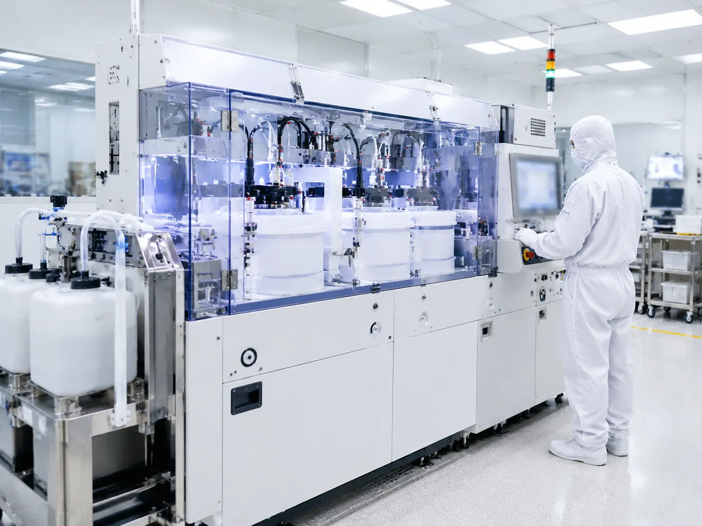
We build our silicon wafer cleaning equipment around modular footprints that scale directly from low-volume pilot lines to continuous high-volume manufacturing. Whether your fab requires an ultra-compact footprint or high-throughput batch automation, our semiconductor wet bench systems adapt to your cleanroom layout without requiring structural retrofits.
Flexible Tool Configurations
-
- Linear Automated Wet Benches: Fully enclosed multi-bath chemical decks featuring overhead servo transfer robots for high-throughput batch immersion.
- Automated Cluster Tools: Enclosed footprint combining chemical immersion, megasonic agitation, and dedicated surface drying modules with central robotic loading.
- R&D and Pilot-Scale Systems: Manual and semi-automated clean stations engineered for university labs, process prototyping, and low-volume substrate qualification.
| Layout Architecture | Target Environment | Footprint (W × D × H) | Handling Capacity |
|---|---|---|---|
| Linear Wet Bench | HVM Production Fabs | 4,200 × 1,800 × 2,400 mm | Up to 50 wafers/run (dual cassette) |
| Automated Cluster | Mid-to-High Volume | 2,800 × 2,200 × 2,300 mm | 25 wafers/batch or continuous single-wafer |
| Manual / Semi-Auto Station | R&D & Failure Analysis | 1,600 × 1,200 × 2,100 mm | Single cassette (25 wafers) manual load |
Central Chemical Distribution (CDS) and Dispense Loops
Seamless chemical routing minimizes operator handling and bath contamination risks:
Direct CDS Tie-Ins: Dedicated supply connections for high-purity bulk chemistries (H2SO4, H2O2, NH4OH, HCl, HF, and IPA) directly integrated into our automated wet bench semiconductor wet processing systems.
Closed-Loop Dosing: Automated spike-dosing units dynamically meter chemical concentrates based on bath operational runtime and inline concentration sensor feedback.
Engineered Slurry Management: Post-CMP configurations feature dedicated slurry dispensing lines with automated DI water flush routines to prevent line clogs and particle build-up.
Commissioning, Target PRE Validation, and SLA Programs
Every tool is installed and qualified on-site by our field engineering team to match strict wafer surface specifications:
-
- Baseline Clean Commissioning: Full on-site verification covering bath thermal stability, laminar flow balancing, and robotic transfer repeatability.
- Particle Removal Efficiency (PRE) Validation: We validate target PRE (>99% at ≥28 nm) using localized defect inspection tools before sign-off.
- Component Life Schedules: Quick-change bath designs, scheduled PFA valve replacements, and seal inspections keep unscheduled downtime under 1.5%.
- SLA & Support: Rapid-response spares kits, on-site recipe development, and Tier-3 engineering escalations to maintain yield and cleanroom tool availability.
Frequently Asked Questions (Silicon Wafer Cleaning Equipment)
How do megasonic systems prevent damage to delicate surface microstructures?
We control acoustic power density and cavitation energy precisely to dislodge sub-micron particles without snapping fragile gate structures or high-aspect-ratio fins.
-
- Frequency Tuning: Operating between 800 kHz and 2 MHz generates small, stable cavitation bubbles rather than aggressive transient cavitation that pits silicon surfaces.
- Uniform Energy Distribution: Direct-coupled transducer arrays distribute acoustic energy evenly across the fluid bath, preventing local hot spots.
- Power Modulation: Pulsed-wave megasonics reduce acoustic streaming pressure during critical FEOL cleans, safeguarding fragile patterns while maintaining high particle removal efficiency (PRE).
What techniques prevent IPA watermark defects on high-aspect-ratio patterns?
Watermarks form when trapped deionized water reacts with dissolved oxygen and silicon during drying. Our single wafer cleaning systems and wet benches counter this via surface-tension-gradient control:
-
- Marangoni Drying: We introduce an ultra-low concentration of heated isopropyl alcohol (IPA) vapor alongside hot nitrogen (N2) over the wet substrate, creating a surface tension gradient that pulls the liquid meniscus downward cleanly off pattern sidewalls.
- Oxygen Exclusion: Chamber nitrogen purging keeps residual oxygen levels in the low parts-per-million range to eliminate silicic acid precipitation.
- Controlled Withdrawal: Regulated vertical lift mechanics withdraw substrates from the rinse bath at steady speeds matching the drying boundary layer.
Can a single wet chemical bench run multiple wafer sizes without retooling?
Yes. We engineer flexible platform architectures across our wet station semiconductor equipment for wafer processing to handle mixed-substrate production environments:
-
- Universal Carrier and End-Effector Kits: Adjustable quartz and PFA cassettes accommodate both 150mm and 200mm wafers (or 200mm and 300mm configurations) using quick-swap inserts.
- Dual-Pitch Transfer Grippers: Automated robotic arms use multi-position edge-grip fingers calibrated for varying substrate thicknesses and diameters.
- Configurable Recipe Metrology: Software profiles automatically adjust immersion bath fluid levels, chemical flow rates, and spin rates based on the recognized cassette load recipe.
How does automated spike dosing extend bath life while maintaining process margins?
Static chemical baths degrade rapidly due to chemical evaporation, wafer drag-out, and active component depletion. Automated spike dosing stabilizes bath chemistry for longer production runs:
-
- Real-Time Chemical Concentration Monitoring: In-line NIR sensors and conductivity meters continuously analyze bath constituents (such as NH4OH and H2O2 in SC-1 solutions).
- Closed-Loop Micro-Dosing: When active component levels drop below preset process thresholds, high-precision metering pumps inject exact chemical spikes directly into the circulation loop.
- Controlled Bleed-and-Feed: Small volumes of spent chemistry are periodically purged while fresh chemicals are added, reducing chemical waste by up to 40% while preventing process drift and cross-contamination.