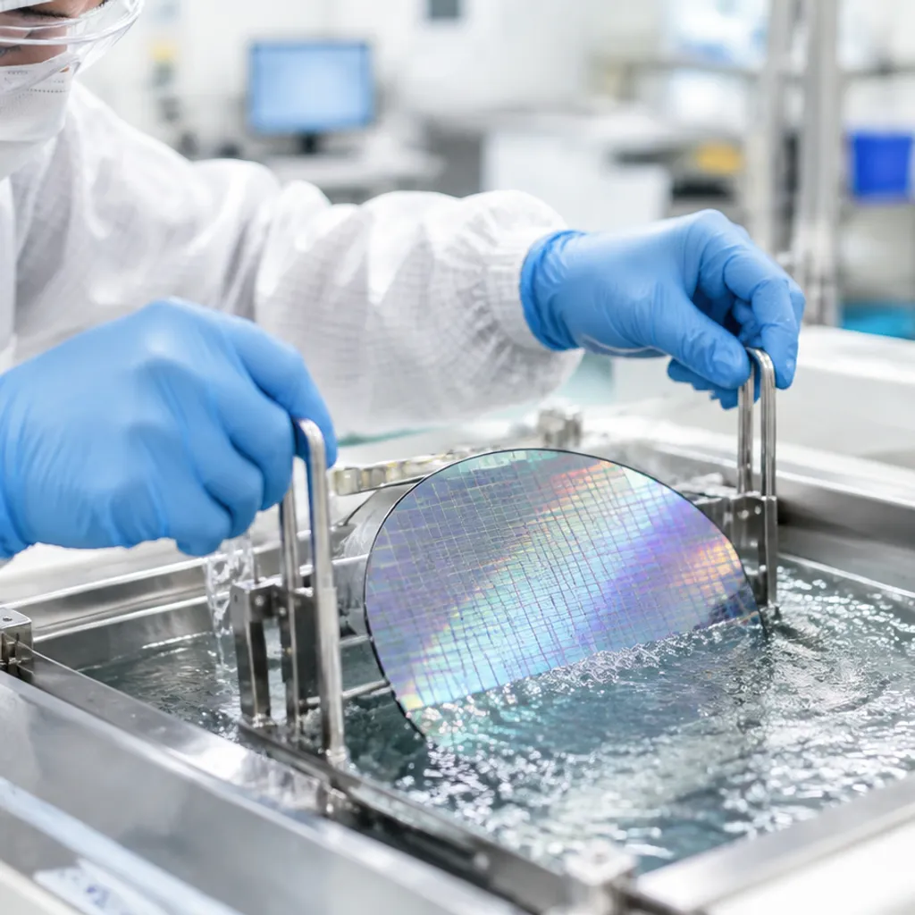
Formula details
Product Details
Overview
How Our Megasonic Wafer Cleaning System Works
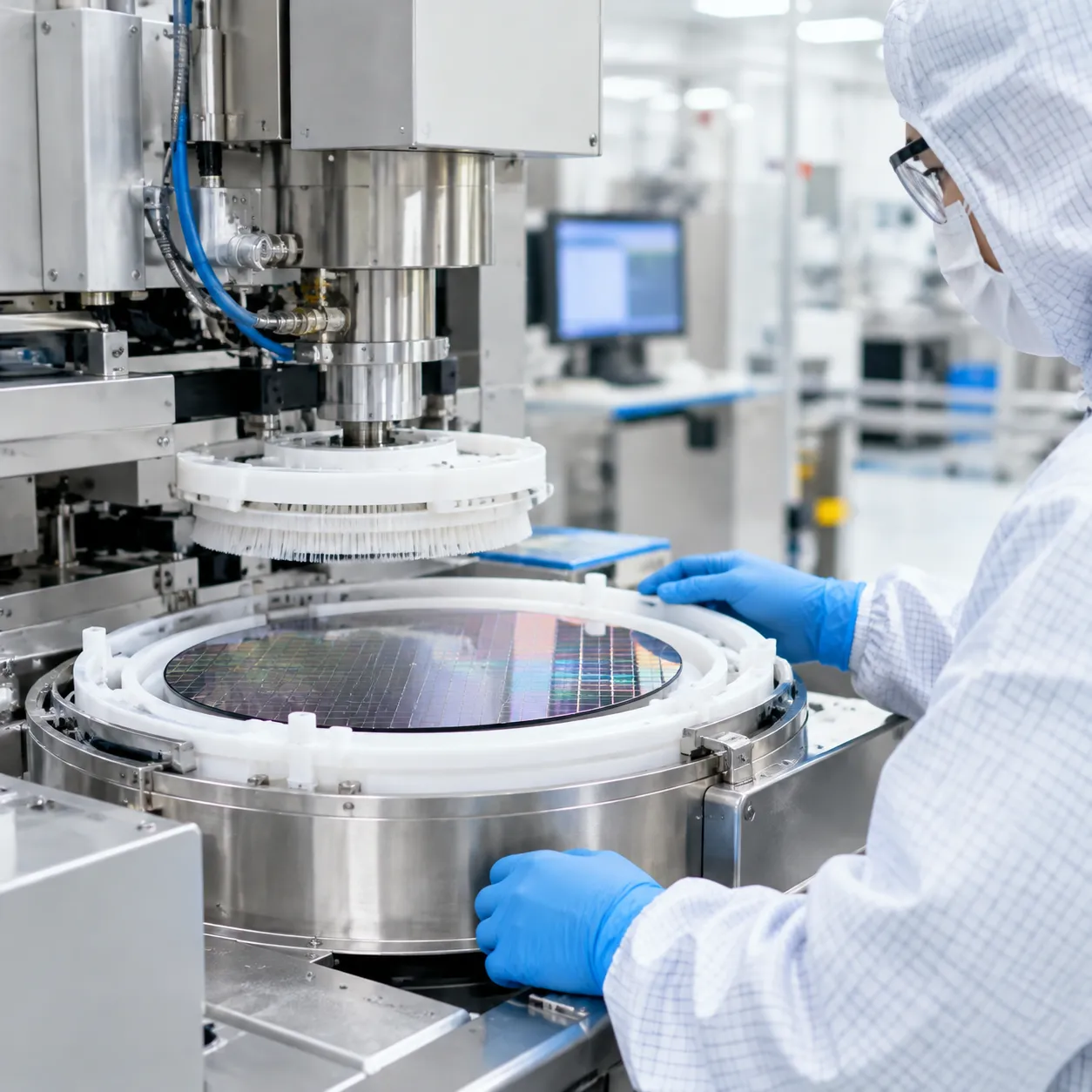
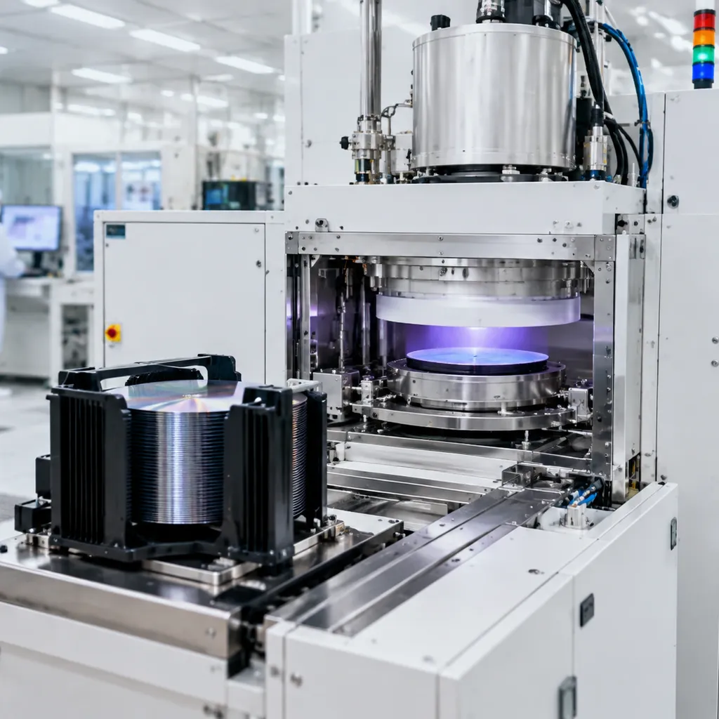
Our megasonic wafer cleaning system combines high-frequency acoustic energy with advanced fluid mechanics to eliminate sub-micron contaminants without damaging sensitive microstructures. By operating in the 700 kHz to 3 MHz frequency regime, our systems deliver targeted cleaning action that overcomes the adhesion forces binding ultra-fine nanoparticles to wafer surfaces.
Controlled Acoustic Cavitation and Micro-Streaming Mechanics
-
- Acoustic Streaming: High-frequency sound waves propagate through the liquid cleaning medium, generating controlled micro-scale acoustic streaming velocities (Schlichting and Eckart streaming).
- Controlled Cavitation: Operates above the cavitation threshold of transient violent collapse, maintaining stable cavitation bubbles that pulsate without producing high-energy shockwaves.
- Particle Dislodgement: The shear stress generated by fluid motion overcomes Van der Waals and electrostatic forces, lifting sub-micron and sub-10nm particles from the substrate.
Boundary Layer Thinning Without Pattern Collapse
Standard hydrodynamic wet cleaning leaves a stagnant hydrodynamic boundary layer on the wafer surface, shielding nano-particles from chemical and mechanical forces.
-
- Hydrodynamic Layer Reduction: Megasonic acoustic streaming compresses the boundary layer thickness down to sub-micron dimensions.
- Structural Integrity Protection: By avoiding transient cavitation collapse, our technology eliminates the pressure spikes that cause pattern collapse, line bending, or material loss on high-aspect-ratio patterns.
- Enhanced Chemical Replenishment: Acoustic streaming continuously forces fresh chemistry directly to the wafer interface, accelerating reaction rates for higher defect removal.
Closed-Loop Digital Generators and Piezoelectric Transducer Arrays
-
- Multi-Element Transducers: High-grade piezoelectric transducer arrays ensure uniform acoustic pressure wave distribution across the entire cleaning field.
- Automatic Frequency Tracking: Digital megasonic power generators dynamically adjust frequency and match impedance in real time, compensating for temperature shifts, bath load changes, and chemistry variations.
- Precision Power Modulation: Closed-loop power control permits micro-watt resolution tuning, maintaining exact acoustic energy levels tailored to specific substrate sensitivities.
Fluid-Coupled Sweep Arms, Nozzles, and Immersion Plate Configurations
Our megasonic wafer cleaner designs adapt to varied process requirements via multiple delivery architectures:
Single-Wafer Sweep Arms: Dynamic motorized sweep arms equipped with specialized megasonic nozzles deliver uniform energy over spinning wafers.
Face-Down / Face-Up Direct Nozzles: Continuous fluid-coupled streams deliver energy directly to the wafer surface for localized defect removal.
Immersion Plate Transducers: Bottom-mounted, side-mounted, or immersible transducer plates generate homogeneous acoustic fields across entire wafer batches in wet process tanks.
Megasonic Wafer Cleaning System Configurations

Single-Wafer Megasonic Cleaning Modules with Dynamic Sweep Arms
Our single-wafer megasonic cleaning tools deliver targeted acoustic energy directly onto rotating wafer surfaces to maximize particle removal without mechanical contact:
-
- Dynamic Sweep Arm Integration: Fluid-coupled megasonic nozzles and sweep arms distribute uniform acoustic waves across the entire substrate from center to edge.
- Controlled Energy Delivery: Eliminates pattern collapse on fragile, high-aspect-ratio microstructures across 50 mm to 300 mm substrates.
- Process Flexibility: Fully compatible with our single-wafer wet clean system for precision cleaning, supporting face-up processing with integrated chemical dispensing and spin-rinse cycles.
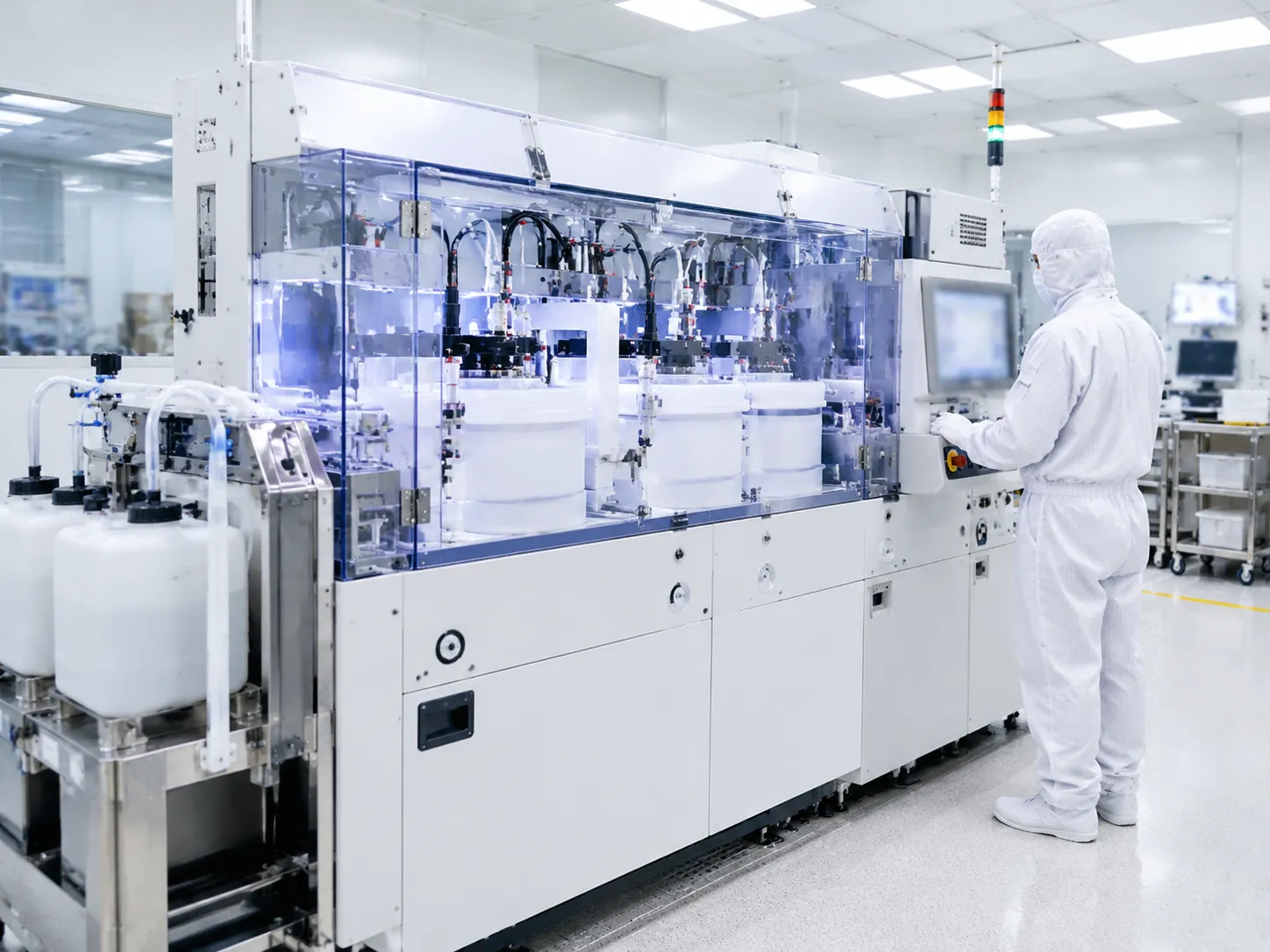
Batch Immersion Wet Benches and Megasonic Tanks
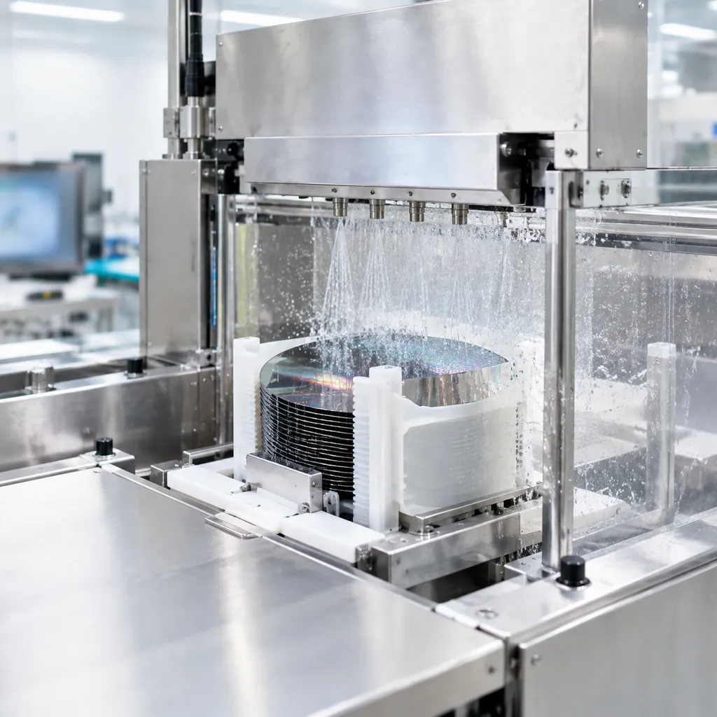
For high-throughput front-end and back-end manufacturing, our batch immersion systems deliver high particle removal efficiency across full wafer cassettes:
-
- Uniform Tank Agitation: Immersible, side-mounted, or bottom-mounted piezoelectric plate transducers distribute balanced acoustic streaming throughout the bath.
- Chemical Compatibility: Built with corrosion-resistant, high-purity materials including PTFE, PFA, PVDF, and quartz to handle SC-1, SC-2, DHF, and solvent chemistries.
- Seamless Automation: Designed as standalone immersion units or fully integrated stations inside an automated chemical wet bench for wafer cleaning and etching.
Retrofit Megasonic Transducers and OEM Generator Components
We supply drop-in megasonic transducers and digital power generators to upgrade existing semiconductor wet process equipment:
-
- Digital Megasonic Generators: High-frequency power supplies (700 kHz to 3.0 MHz) equipped with automatic frequency tracking and closed-loop impedance matching.
- Transducer Arrays: Custom-machined plate and nozzle transducers engineered to replace legacy ultrasonic or megasonic units without altering existing tank architecture.
- Consistent Power Modulation: Stable output prevents standing wave hot spots, extending transducer service life and stabilizing wafer surface yields.
Key Technical Features of Our Megasonic Cleaner
Uniform Acoustic Field Distribution
Standard megasonic setups often suffer from hot spots and dead zones caused by stationary acoustic patterns. We use dynamic frequency sweeping and multi-element transducer arrays to eliminate standing wave nodes. This ensures:
Homogeneous acoustic pressure across the entire wafer surface.
Elimination of localized energy spikes that cause gate oxide punch-through.
Consistent boundary-layer thinning on center-to-edge wafer zones.
Low-Wattage Digital Power Modulation
Cleaning advanced nodes with high aspect ratios requires soft cavitation. Our closed-loop digital generators provide ultra-precise power modulation at low wattage increments, ensuring:
Controlled acoustic streaming without transient violent cavitation.
Safe particle removal on fragile, sub-10nm fin structures and MEMS cantilevers.
Real-time impedance matching to stabilize power output during fluid flow fluctuations.
High-Purity Wetted Materials and Chemical Flexibility
Process integrity depends on inert fluid pathways. We build all process-wetted components from ultra-pure fluoropolymers and virgin quartz, preventing trace metal leaching and ionic contamination. Following the principles outlined in our semiconductor wet bench design and specification guide, our systems seamlessly integrate with both aggressive acidic and solvent chemistries.
| System Feature | Engineering Capability | Process Compatibility |
|---|---|---|
| Acoustic Field Uniformity | Variation < ±3% with auto-frequency tracking | Single-wafer dynamic arms & batch immersion tanks |
| Digital Power Control | Sub-watt power stepping from 700 kHz to 3.0 MHz | Damage-free cleaning for fragile FEOL/BEOL patterns |
| Corrosion-Resistant Hardware | High-purity PTFE, PFA, PVDF, and quartz construction | Compatible with SC-1, SC-2, DHF, SPM, and solvents |
| Fluid Coupling Mechanics | Direct liquid meniscus and immersion boundary thinning | Ultra-pure water (UPW) rinsing, post-CMP slurry removal |
Megasonic Wafer Cleaning System Technical Specifications
| Specification Parameter | Standard Platform Capability |
|---|---|
| Wafer Form Factors | 50 mm, 100 mm, 150 mm, 200 mm, and 300 mm (2" to 12") |
| Operating Frequency | 700 kHz to 3.0 MHz (Multi-frequency digital tracking) |
| Particle Removal Target | Sub-micron down to sub-10 nm particles |
| Cleanroom Rating | ISO Class 1 compatible |
| Fab Automation | SECS/GEM (SEMI E5, E30, E37 compliant) |
| Wetted Materials | High-purity PFA, PTFE, PVDF, and optical-grade quartz |
Substrate Compatibility from 50 mm to 300 mm
Our systems handle standard silicon, compound semiconductors (SiC, GaN, GaAs), and photomasks across all industry dimensions. Whether configured for smaller substrates or integrated into automated semiconductor wet processing systems for 300mm wafers, the platform maintains complete mechanical and fluid stability during full-cycle processing.
Multi-Frequency Acoustic Control (700 kHz – 3.0 MHz)
-
- Real-Time Impedance Matching: Dynamic frequency sweep and auto-tuning eliminate dead zones and standing wave nodes across the wafer surface.
- Tunable Power Densities: Low-wattage modulation allows precise cavitation control to protect high-aspect-ratio patterns and thin-film structures from acoustic stress.
Sub-10 nm Particle Removal Efficiency (PRE)
By thinning the fluid boundary layer via high-frequency micro-streaming, our megasonic cleaner lifts sub-micron and sub-10 nm contaminants without substrate pitting or physical damage.
Fab Automation and ISO Class 1 Cleanroom Readiness
-
- SECS/GEM Integration: Fully compliant with SEMI E5, E30, and E37 standards for seamless host communication, inline recipe tracking, and automated wet bench interfacing.
- Enclosed Mini-Environment: Designed for direct integration into ISO Class 1 fab cleanrooms, complete with automated chemical delivery and ultra-pure fluid pathways.
Semiconductor Wet Cleaning Applications
Our megasonic wafer cleaning system provides targeted, damage-free acoustic energy across a broad spectrum of front-end and back-end fab operations. By combining precise acoustic streaming with high-purity chemical processing, we solve yield-limiting contamination issues across diverse substrate types and process nodes.
FEOL Pre-Gate Oxide and STI Pre-Cleaning
Front-End-of-Line (FEOL) processes demand strict particle defect control without altering delicate surface roughness:
Pre-Gate Oxide Cleans: Removes trace organic residues and sub-micron particulate matter before gate dielectric growth.
Shallow Trench Isolation (STI): Cleans trench sidewalls and corners thoroughly, thinning the hydrodynamic boundary layer to lift nanoparticles without damaging fragile silicon fins.
Native Oxide Etch Support: Pairs with dilute hydrofluoric (DHF) chemistries to strip uniform oxide layers while keeping particle redeposition near zero.
BEOL and Post-CMP Slurry Particle Removal
Chemical Mechanical Planarization leaves stubborn colloidal silica, ceria, and alumina residues embedded on wafer surfaces. Our advanced cleaning technology accelerates residue lift-off during Back-End-of-Line (BEOL) steps:
Post-CMP Slurry Scrubbing: High-frequency megasonic waves dislodge tightly adhered nanoscale abrasive particles from copper interconnects and low-k dielectric surfaces.
Corrosion-Free Metal Cleaning: Operates under controlled acoustic power densities to prevent pitting, galvanic corrosion, or delamination on exposed metal lines.
Compound Semiconductor Substrate Cleaning (SiC & GaN)
Wide-bandgap materials feature high mechanical hardness and unique surface chemistry challenges:
Silicon Carbide (SiC) & Gallium Nitride (GaN): Cleans epi-ready substrates and thinned wafers without inducing micro-scratches or subsurface lattice damage.
Post-Grind/Post-Polish Decontamination: Eliminates heavy particulate loading after mechanical planarization, maximizing epitaxial yield on high-value power semiconductor substrates.
Photomask, Reticle, and MEMS/NEMS Release Cleaning
Delicate, high-aspect-ratio microstructures require ultra-gentle cleaning forces:
Photomask and Reticle Cleaning: Cleans critical optical and EUV reticle surfaces without causing phase-shift degradation or absorber pattern erosion.
MEMS/NEMS Cantilever Release: Dislodges process debris during critical release stages, eliminating stiction and preventing structural pattern collapse on fragile suspended beams.
Yield Validation and Particle Removal Performance
We validate every megasonic wafer cleaning system using rigorous particle metrics and acoustic characterization to safeguard your production line from yield loss.
Heating Chamber
Continuous Hot Zone
↓
Vacuum Isolation Gate
↔ Rapid Workpiece Transfer
↓
Quench / Load Chamber
Oil Bath / Gas Quenching
Particle Removal Efficiency (PRE) vs. Power Density Benchmarks
Our systems hit >99.2% PRE on sub-micron and fine slurry residues without requiring aggressive acoustic power. By precisely tuning frequency modulation against power density, our megasonic wafer cleaner removes sticky contaminants while preventing cavitation-induced surface pitting across standard silicon and advanced power semiconductor substrates.
Acoustic Field Mapping and Energy Uniformity
We eliminate dead zones and localized hot spots that cause uneven cleaning or localized wafer damage:
Uniform Field Distribution: Acoustic power variation remains strictly within < ±3% across the entire substrate surface.
Hydrophone Mapping: Every transducer array is calibrated via multi-point hydrophone field scans to verify uniform sound pressure.
Controlled Streaming: Consistent acoustic streaming guarantees repeatable boundary layer thinning from the center to the wafer bevel.
Zero Structural Damage on High-Aspect-Ratio Patterns
Cleaning fragile microstructures demands clean, low-impact acoustic energy transfer. We verify damage-free processing on sensitive high-aspect-ratio structures (HAR > 15:1), ensuring:
Complete particulate release down to sub-10 nm nodes.
Elimination of destructive transient cavitation bursts.
Zero pattern collapse or line-bending on delicate gates and fins.
Quality Assurance and Fab Compliance Standards
Our megasonic wafer cleaning systems are engineered to integrate cleanly into automated semiconductor cleanrooms. We apply strict manufacturing controls and testing protocols to ensure our equipment meets international standards for cleanroom safety, purity, and operational reliability.
-
- SEMI S2, SEMI S8, and CE Safety Compliance: Every system adheres to SEMI S2 environmental, health, and safety standards and SEMI S8 ergonomic design criteria, alongside CE compliance. You can review our full spectrum of cleanroom and manufacturing standards via our fab quality and safety certifications.
- Ultra-Pure Fluid Delivery & Helium Leak-Tested Lines: All chemical-wetted pathways utilize high-purity PFA, PTFE, and PVDF materials. Fluid manifolds and delivery circuits undergo rigorous helium leak testing prior to delivery, preventing chemical micro-leaks and fluid contamination in sub-micron processes.
- SEMI E5 (SECS-II), E30 (GEM), and E37 (HSMS) Integration: Our digital control architecture supports standard fab host communication interfaces, enabling remote recipe management, automated lot tracking, real-time power monitoring, and continuous fault diagnostics.
Custom Engineering and Application Support
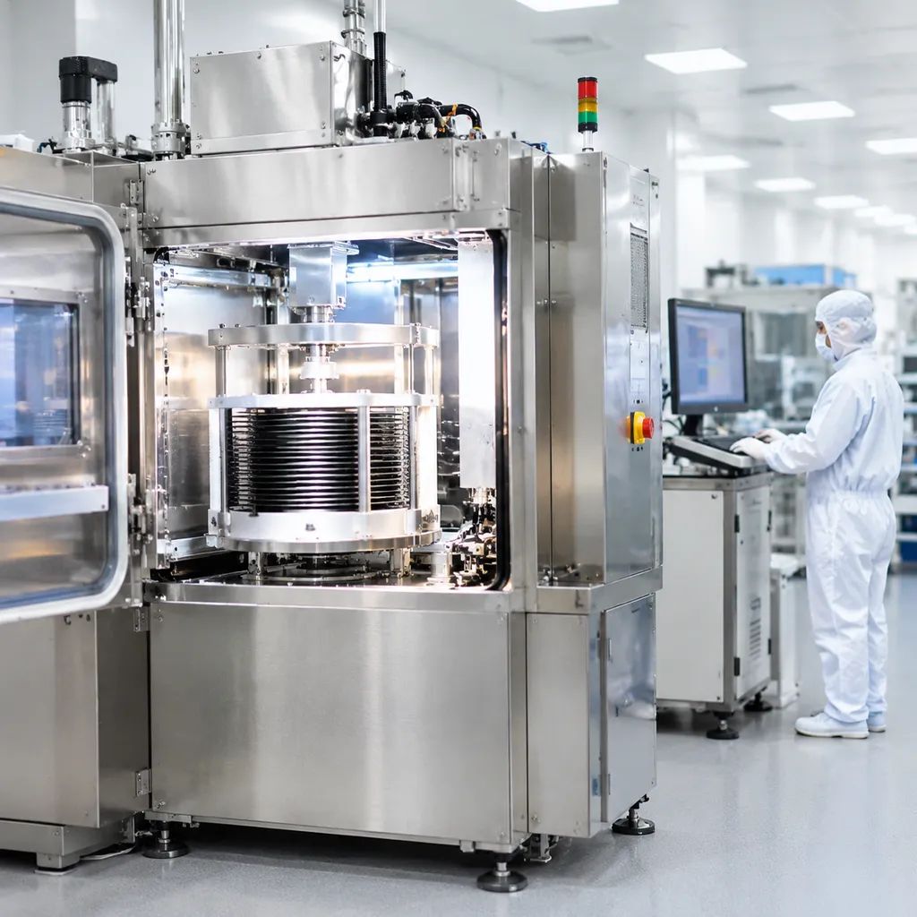
Every fab and pilot line runs unique processes. We configure our megasonic wafer cleaning system hardware and process parameters to match specific wet-bench footprints, chemical workflows, and substrate form factors.
Custom Tank and Transducer Sizing for Non-Standard Substrates
Standard platforms do not always fit specialized R&D or compound semiconductor production. We design tailor-made process tanks, dynamic sweep arms, and immersible transducer plates to fit non-standard parts and production environments:
Substrate Versatility: Custom fixtures for square substrates, ultra-thin wafers, glass panels, optical components, and thick SiC/GaN boules.
Form-Factor Matching: Modular transducer plates engineered for bottom-mounted, side-mounted, or direct-nozzle chemical delivery.
Custom Wet Benches: Seamless integration into existing automated or manual wet lines used across advanced semiconductor manufacturing applications.
Recipe Development and Chemistry Optimization
Our dedicated application labs help process teams qualify cleaning chemistry and acoustic settings before fab deployment:
Cavitation & Streaming Tuning: Fine-tuning acoustic frequency and power density to eliminate sub-micron defects without surface etching or pattern damage.
Chemistry Compatibility Trials: Evaluating SC-1, SC-2, dilute HF, surfactant blends, and solvent interactions on test wafers.
Defect Metrology & PRE Testing: Full pre- and post-clean particle mapping to validate particle removal efficiency (PRE) for critical wafer fabrication steps.
Preventive Maintenance and Quick-Turn Replacement Components
Tool downtime directly cuts fab throughput. We provide dedicated lifecycle support to keep your megasonic cleaner semiconductor equipment running at peak performance:
Quick-Swap Transducers & Generators: Pre-tuned piezoelectric transducers and digital megasonic generators ready for immediate drop-in replacement.
Field Calibration & Acoustic Mapping: Regular acoustic field uniformity checks and impedance recalibration to maintain steady cleaning energy across every batch.
Global Spare Parts Inventory: Stocked fluid lines, PTFE/PFA valves, seals, and RF cables shipped with rapid turnaround times.
Frequently Asked Questions About Megasonic Wafer Cleaning Systems
What is the difference between ultrasonic and megasonic wafer cleaning?
While both technologies use acoustic energy to remove contaminants, their operating frequency and cleaning mechanisms differ fundamentally:
| Parameter | Ultrasonic Cleaning | Megasonic Cleaning |
|---|---|---|
| Operating Frequency | 20 kHz – 100 kHz | 700 kHz – 3.0 MHz |
| Primary Mechanism | Transient cavitation (bubble implosion) | Acoustic streaming & controlled micro-cavitation |
| Particle Size Target | Micron-scale (> 1 µm) | Sub-micron & sub-10 nm particles |
| Wafer Pattern Risk | High risk of surface pitting and collapse | Damage-free for delicate, high-aspect-ratio nodes |
How does megasonic cleaning prevent pattern collapse on fragile sub-10nm nodes?
Our megasonic wafer cleaning system operates above cavitation thresholds where destructive bubble implosions occur. Instead, high-frequency acoustic waves generate rapid micro-streaming flows that thin the liquid boundary layer across the substrate. This acoustic push dislodges nano-scale contaminants via hydrodynamic drag force rather than violent shockwaves, preserving fragile structures and preventing pattern collapse.
Can this megasonic system handle both single-wafer and batch processing?
Yes. We configure our acoustic cleaning technology for both production styles:
Single-Wafer Processing: Integrated dynamic sweep arms and megasonic nozzles for high-precision processing on our single-wafer wet processing equipment for 300mm fabs.
Batch Processing: Immersible and bottom-mounted transducer plates engineered for batch immersion wet bench systems targeting high-volume manufacturing lines.
What chemistries are compatible with your megasonic cleaning tools?
All fluid-contact surfaces are constructed from ultra-pure, corrosion-resistant polymers and materials, including PTFE, PFA, PVDF, and quartz. Our megasonic cleaners reliably support:
Standard RCA cleans (SC-1 ammonium hydroxide/hydrogen peroxide and SC-2 hydrochloric acid/peroxide)
Dilute hydrofluoric acid (DHF) for native oxide etching
Ultra-pure water (UPW) rinse cycles
Post-CMP specialty cleaning chemicals and solvent-based chemistries
How does the system ensure uniform acoustic energy across 300mm wafers?
We achieve uniform energy distribution across the entire substrate by combining digital frequency-tracking generators with advanced transducer array designs. In single-wafer modules, recipe-controlled sweep arm speeds compensate for radial linear velocity changes from wafer center to edge. In batch immersion tanks, multi-frequency modulation eliminates standing wave nodes, preventing localized energy hotspots and delivering consistent particle removal efficiency across every wafer in the carrier.