Fundamental Principles of Semiconductor Etching
Key Etch Performance Metrics: Etch Rate and Uniformity (WIW/WTW)
The foundation of any etching process begins with material removal speed and spatial consistency across the wafer surface:
-
- Etch Rate (ER): The thickness of material removed per unit time, typically measured in angstroms per minute (Å/min) or nanometers per minute (nm/min). A stable etch rate ensures predictable process recipes.
- Within-Wafer Uniformity (WIW): Measures variation in etch depth across a single wafer from center to edge. Poor WIW uniformity directly degrades device performance across dies.
- Wafer-to-Wafer Uniformity (WTW): Tracks process drift across consecutive fabrication batches. Maintaining tight WTW control requires stable chemical baths in wet benches or steady RF power and gas flows in plasma chambers.
Selectivity and Mask Protection
Selectivity (S) defines an etch process's ability to remove the target film while leaving the protective mask (photoresist, hard mask) and underlying substrate untouched:
Selectivity (S) = Etch Rate of Target Material / Etch Rate of Mask or Substrate
-
High Selectivity (S ≫ 10:1): Common in wet chemical etching, where liquid solutions selectively dissolve oxides or metals without attacking silicon or resist.
-
Mask Integrity: High selectivity prevents mask erosion, pinhole creation, and punch-through to the substrate, safeguarding delicate structural layers.
Directionality, Anisotropy, and Profile Control
How an etch proceeds geometrically dictates the shape of the resulting profile. Understanding isotropic vs. anisotropic semiconductor etching is fundamental when choosing between chemical and plasma-based solutions:
-
Isotropic Etching: Material is removed at equal rates in all directions (vertically and horizontally), producing rounded sidewalls and mask undercuts.
-
Anisotropic Etching: Material removal is strictly directional—predominantly vertical—yielding straight, vertical sidewalls essential for tight-pitch microelectronics.
-
Degree of Anisotropy (A): Quantified using vertical etch rate (Rᵥ) and lateral etch rate (Rₗ):
A = 1 − (Rₗ / Rᵥ)
An ideal anisotropic process has A = 1 (Rₗ = 0), whereas a purely isotropic process has A = 0 (Rₗ = Rᵥ).
Etch Bias and Lateral Undercut Mechanics
When chemical reactants penetrate underneath the photoresist pattern, they cause lateral undercut, leading to etch bias:
-
- Etch Bias: The dimensional difference between the original lithography mask dimension and the actual physical feature width after etching.
- CD Loss: Severe lateral undercut shrinks the critical dimension (CD) of lines or expands trench openings, creating catastrophic pattern collapse or electrical failure.
- Balancing Bias: In advanced silicon wafer patterning, comparing wet etching vs dry etching semiconductor techniques often comes down to managing this undercut—leveraging isotropic wet chemistry for clean releases and directional dry plasma for zero-bias vertical trenches.
Wet Chemical Etching in Semiconductor Manufacturing
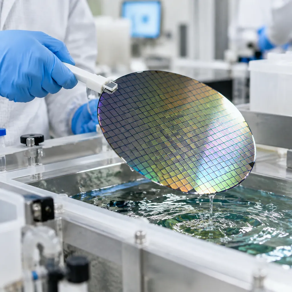
Wet chemical etching remains an essential pillar in semiconductor wafer processing, delivering high throughput and superior chemical selectivity where directional ion bombardment is unnecessary. In wafer fabrication, we rely on liquid-phase solutions to dissolve unmasked substrate areas through controlled chemical reactions.
Reactant Diffusion ➔ Surface Adsorption ➔ Chemical Reaction ➔ Desorption ➔ Byproduct Diffusion
Mechanism of Liquid-Phase Etching and Transport Regimes
The etching process follows two primary kinetic mechanisms:
-
- Reaction-Rate-Limited Regime: The etch rate depends strictly on chemical reaction speed and bath temperature. This regime provides uniform etching across the wafer surface because fluid movement variations do not dictate material removal.
- Diffusion-Limited Regime: The etch rate depends on how quickly fresh reactants reach the surface and how fast dissolved byproducts diffuse away. We control this regime using precise chemical recirculation, agitation, or dynamic spray nozzles to prevent non-uniform etching across dense patterns.
Common Wet Etch Chemistries
Selecting the right chemistry determines etch rate selectivity and surface finish:
-
Hydrofluoric Acid (HF) and Buffered Oxide Etch (BOE): Standard solutions for silicon dioxide (SiO₂) stripping without attacking underlying silicon substrates.
-
Hot Phosphoric Acid (H₃PO₄): Operates at elevated temperatures (typically 150°C to 180°C) to strip silicon nitride (Si₃N₄) selectively over oxide and silicon.
-
Potassium Hydroxide (KOH) and TMAH: Anisotropic wet etchants for crystalline silicon, etching the (100) crystal plane faster than the (111) plane to form precise micro-cavities.
-
HNA (Hydrofluoric, Nitric, and Acetic Acid): Formulates an isotropic silicon etch system via oxidation followed by oxide dissolution.
Core Advantages in Wafer Fabrication
When evaluating wet and dry etching semiconductor workflows, wet systems excel in specific manufacturing steps:
-
- Exceptional Etch Rate Selectivity: Liquid chemistries dissolve target films while stopping abruptly on thin underlying stop layers, preserving delicate gate oxides or silicon barriers.
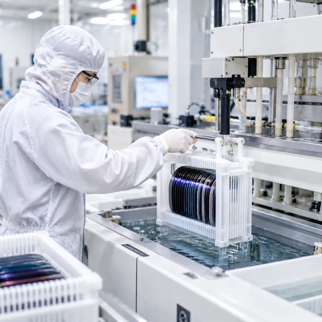
- High Fab Throughput: Processing multiple wafers simultaneously in an automated chemical wet bench for wafer cleaning and etching maximizes batch wafer yield at a lower operating cost.
- Zero Plasma-Induced Damage: Liquid processing eliminates charge buildup, lattice damage, and ion-bombardment stress associated with vacuum plasma environments.
Process Limitations and Challenges
Understanding the tradeoffs of wet etching vs dry etching semiconductor processing prevents yield loss:
-
- Isotropic Undercutting: Most wet solutions etch equally in all directions, creating lateral undercut beneath the photoresist mask and limiting wet etching on sub-micron critical dimensions.
- Pattern Collapse: As microstructures become narrower and taller, liquid surface tension during rinsing and drying exerts capillary forces that can pull fine features together.
- Chemical Consumption & Safety: Aggressive acids require dedicated containment, precise bath replenishment systems, and rigorous chemical waste neutralization. For specialized laboratory lots or dedicated production runs, utilizing a purpose-built precision wafer etching system ensures uniform chemical delivery and safe fluid handling.
Dry Plasma and Vapor-Phase Etching Explained
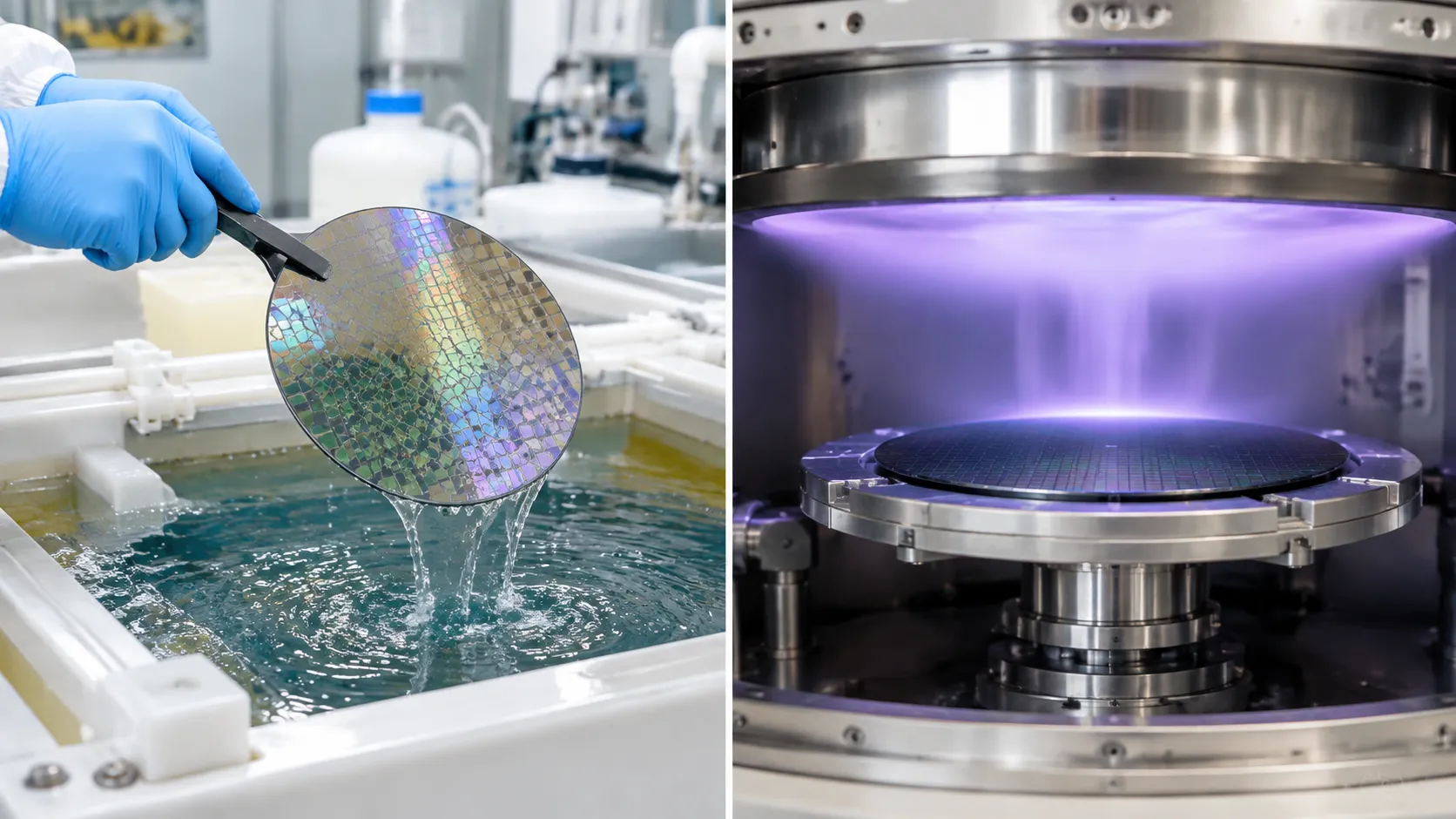
In modern microfabrication, dry plasma etching is the foundation of high-density pattern transfer. When we look at wet and dry etching semiconductor workflows, dry processing takes over whenever feature sizes shrink below the limits of liquid chemical surface tension. Instead of liquid baths, dry systems use gas-phase chemistry, RF glow discharges, and energetic ions to etch target thin films with nanometer-level precision.
Dry Etch Mechanisms: Radicals, Sputtering, and RIE
Dry etching relies on three distinct physical and chemical mechanisms:
-
- Chemical Radical Etching: Neutral gas radicals (like fluorine or chlorine atoms) react chemically with the wafer surface to create volatile byproducts. This mode provides high material selectivity but remains largely isotropic.
- Physical Sputtering: Energetic inert gas ions (such as Ar⁺) are accelerated across an RF plasma sheath to physically knock atoms off the substrate. This creates directional, vertical sidewalls but suffers from low selectivity and mask erosion.
- Reactive Ion Etching (RIE): The standard in wafer fabrication. RIE combines chemical radicals with directional ion bombardment. The ions weaken surface bonds and remove passivation layers on horizontal planes, allowing chemical radicals to rapidly etch downward while leaving sidewalls protected.
Main Configurations: CCP, ICP-RIE, and Bosch DRIE
Plasma etch reactors are tailored to specific material stacks and aspect ratios:
-
- Capacitively Coupled Plasma (CCP): Uses parallel RF electrodes to generate plasma. It produces high ion energies, making it ideal for dielectric etching (SiO₂, SiN) and hard mask patterning.
- Inductively Coupled Plasma (ICP-RIE): Uses an inductive coil to generate high-density plasma independently of the substrate bias. This enables high etch rates at lower chamber pressures and reduced ion damage.
- Bosch Deep Reactive Ion Etching (DRIE): A switched process that cycles between chemical etching (SF₆) and polymer sidewall passivation (C₄F₈). This configuration achieves vertical trenches with aspect ratios exceeding 30:1 for MEMS devices and Through-Silicon Vias (TSVs).
Advantages: Anisotropic Profiles and CD Control
When comparing wet etching vs dry etching semiconductor lines, dry plasma etching delivers critical capabilities for front-end-of-line (FEOL) and advanced packaging:
-
- Anisotropic Profile Control: Directional ion acceleration eliminates lateral undercut, enabling vertical sidewalls and high-aspect-ratio trench definition.
- Critical Dimension (CD) Retention: Tightly regulates sub-micron gate widths and pitch scaling without mask lifting.
- No Surface Tension Limitations: Gas-phase reactants penetrate narrow nanoscale gaps without the risk of pattern collapse caused by liquid capillary forces.
Process Drawbacks: Selectivity, PID, and Tool Cost
Despite its patterning resolution, dry etching introduces specific engineering challenges:
-
- Reduced Etch Rate Selectivity: Energetic ion bombardment inherently attacks underlying stop layers and photoresist masks faster than chemical wet baths.
- Plasma-Induced Damage (PID): Ultraviolet radiation and high-energy ion impacts can create crystal lattice defects, surface roughness, and gate oxide charge trapping.
- High Capital and Operating Cost: Vacuum load locks, turbomolecular pumps, RF matching networks, and toxic gas handling systems significantly raise tool cost.
Balancing these dry plasma steps with specialized wet chemical clean benches and advanced semiconductor wafer etching equipment ensures consistent yield, defect-free interfaces, and minimal sidewall damage across the entire fabrication sequence.
Wet Etching vs. Dry Etching Semiconductor: Direct Comparison
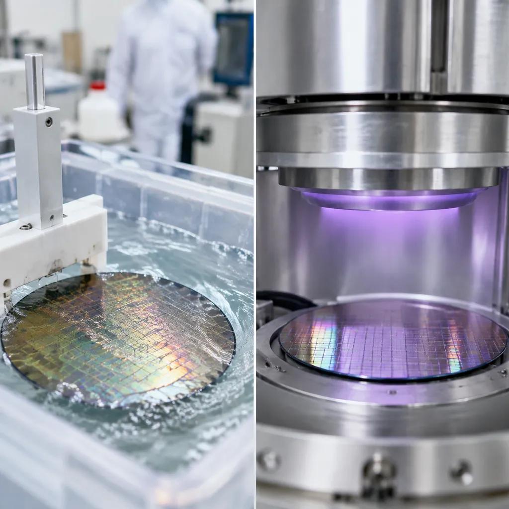
Side-by-Side Performance Matrix
| Metric | Wet Chemical Etching | Dry Plasma Etching (RIE / ICP) |
|---|---|---|
| Primary Mechanism | Liquid-phase chemical reaction | Ion bombardment & reactive gas radicals |
| Profile & Directionality | Isotropic (multi-directional) | Anisotropic (highly directional vertical walls) |
| Etch Rate Selectivity | Very high (>100:1 to mask/underlayer) | Moderate to tunable (typically 5:1 to 30:1) |
| Critical Dimension (CD) Control | Limited (>1 µm features) | High precision (sub-micron to nanometer scale) |
| Defect / Damage Mechanism | Surface tension limits, chemical residues | Plasma-induced damage (PID), surface charging |
| Operating Cost & Throughput | High throughput, lower initial capital cost | Lower throughput per chamber, higher capital cost |
Profile Evolution: Isotropic Undercut vs. Anisotropic Straight Walls
In wet and dry etching semiconductor lines, profile control defines mask geometry fidelity:
-
- Isotropic Undercutting (Wet): Chemical baths etch laterally at roughly the same rate as vertically. This creates a rounded undercut beneath the photoresist mask, which works well for full-film stripping and sacrificial layer removal but leads to line loss at sub-micron pitches.
- Anisotropic Sidewalls (Dry): Reactive ion etching uses directional electric fields to drive energetic ions straight down into the wafer. Passivation gases coat the feature sidewalls, preventing lateral attack and maintaining sharp, vertical profiles essential for dense circuitry.
ARDE and Microloading vs. Surface Tension Limits
Both methods encounter physical limits when scaling to aggressive geometries:
-
- Dry Etch Constraints: Feature scaling triggers Aspect Ratio Dependent Etching (ARDE), commonly known as RIE lag. Etch rates slow down inside narrow trenches because neutral radicals struggle to diffuse to the bottom. Dense patterns also suffer from microloading, where localized reactant depletion reduces etch rates compared to open field areas.
- Wet Etch Constraints: High-aspect-ratio wet processing is constrained by fluid dynamics and liquid surface tension. Trapped micro-bubbles and slow chemical exchange can stop localized material removal entirely, making proper chemical delivery configurations essential. When setting up liquid chemical lines, reviewing our batch immersion vs single wafer wet processing comparison helps determine the right agitation and fluid flow strategy for demanding substrate surface treatments.
Process Selection Guide: When to Use Wet vs. Dry Etching
Choosing between chemical liquid baths and vacuum plasma steps defines both device performance and production yield. In wet and dry etching semiconductor workflows, we select the tool based on critical dimension (CD) tolerances, profile requirements, and budget constraints.
Etch Profile Required
| Isotropic (Uniform All Sides) | Anisotropic (Vertical Sidewalls) |
|---|---|
| ↓ | ↓ |
| Wet Chemical Etch | Dry Plasma Etch |
| • Sacrificial release | • Gate patterning |
| • Backside thinning | • Contact holes & STI |
| • Pad oxide strip | • High-aspect TSVs |
Best Applications for Wet Etching
When zero surface damage, bulk removal, and exceptional etch rate selectivity are non-negotiable, liquid-phase processing is the primary choice.
-
- Wafer Backside Thinning and Stress Relief: Rapidly removes bulk silicon without generating lattice defects or sub-surface micro-cracks.
- MEMS Sacrificial Layer Release: Uses isotropic undercutting with chemistry like Buffered Oxide Etch (BOE) or hydrofluoric acid (HF) to free freestanding microstructures without physical ion bombardment.
- Pad Oxide and Hard Mask Stripping: Selectively strips sacrificial silicon dioxide or silicon nitride films (using hot phosphoric acid) while leaving underlying active silicon undisturbed.
- Surface Cleaning and Planar Preparation: Configured inside an acid wet bench for safe chemical processing to clear native oxides and metallic residues prior to thermal diffusion or epitaxy.
Best Applications for Dry Etching
When geometries shrink below sub-micron thresholds, plasma-driven directionality takes priority to eliminate lateral undercut.
-
- Advanced Transistor Gates and FinFET Profiles: Patterning sub-micron poly-silicon and metal gates demands anisotropic profiles to preserve channel lengths.
- High-Density Contact Holes and Vias: Delivers vertical profiles through inter-layer dielectrics (ILD) with precise depth and CD control.
- Shallow Trench Isolation (STI): Cuts steep, controlled silicon trenches to isolate adjacent active transistor areas on the wafer surface.
- Through-Silicon Vias (TSV): Uses Deep Reactive Ion Etching (DRIE) Bosch cycles to drill narrow, high-aspect-ratio holes through the substrate for 3D packaging.
Cost-Per-Wafer and Capital Expenditure Tradeoffs
Balancing wet etching vs dry etching semiconductor toolsets requires evaluating operational throughput against capital costs:
| Parameter | Wet Chemical Etching | Dry Plasma Etching |
|---|---|---|
| Tool Footprint & CapEx | Lower initial capital expenditure; modular tank designs | Higher CapEx due to vacuum systems, RF generators, and turbomolecular pumps |
| Wafer Throughput | High; batch immersion wet bench systems process 25 to 50 wafers simultaneously | Moderate to low; primarily single-wafer chambers to maintain plasma uniformity |
| Consumable & Facility Costs | Higher chemical volume consumption and neutralizer waste treatment | High specialty gas costs (fluorocarbons, chlorine) and vacuum maintenance |
| Yield Vulnerability | Risk of pattern collapse on fine structures due to liquid surface tension | Risk of plasma-induced damage (PID) and chamber drift over extended runs |
Equipment Architecture and Cleanroom Process Integration
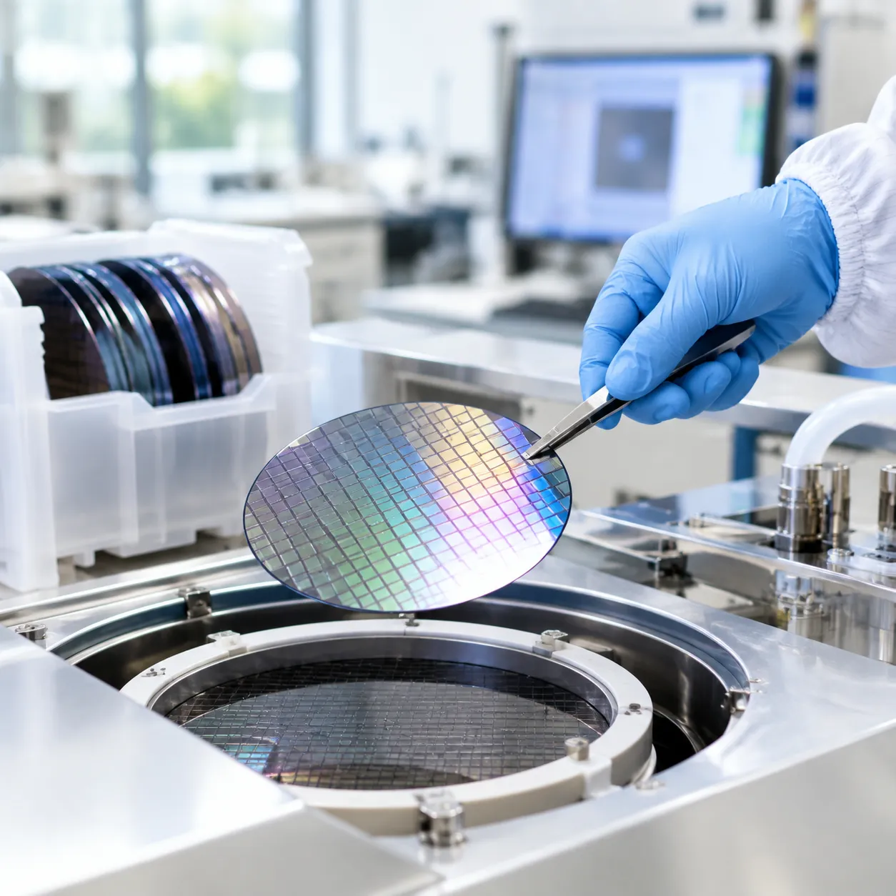
Automated Wet Benches vs. Single-Wafer Spin Processing
Choosing between immersion batch tools and single-wafer spin processors comes down to balancing raw throughput against critical dimension precision:
-
- Automated Wet Benches: Ideal for batch processing (typically 25 to 50 wafers per lot). Using automated wet bench semiconductor wet processing systems, we achieve high throughput for bulk chemical etching, wafer stripping, and batch oxide removal while keeping chemical replenishment costs low.
- Single-Wafer Spin Processors: Designed for tight boundary-layer control. Dispensing fresh chemistry directly onto a rotating substrate delivers exceptional within-wafer uniformity (WIW) and eliminates cross-contamination on critical layers.
Managing Contamination, Micro-Bubbles, and Marangoni Drying
In liquid-phase processing, surface-tension anomalies and trapped micro-bubbles directly lead to unetched spots and yield loss:
-
- Bubble Mitigation: Continuous chemical recirculation and degassing systems prevent gas entrapment inside high-aspect-ratio patterns.
- Fluid Agitation: Controlled megasonic agitation and spray delivery refresh the boundary layer constantly.
- Surface Drying: Standard spin-rinse dryers often cause water marks on fine patterns. Utilizing isopropyl alcohol (IPA) vapor with Marangoni drying eliminates surface-tension gradients, protecting fragile structures from pattern collapse.
Bridging Wet and Dry Steps: Surface Preparation and Post-Dry Etch Cleans
Balancing wet etching vs dry etching semiconductor workflows is essential for high-yield device fabrication. Plasma etching leaves behind tough sidewall polymer residues, fluorocarbon passivations, and localized substrate damage.
We pair dry plasma steps with specialized wet bench chemistry equipment for semiconductor cleanroom operations. A quick, highly selective wet clean strips halogenated polymers and post-etch ash residues without attacking the underlying dielectric or critical gate features, restoring an ultra-clean surface ready for subsequent deposition.
Frequently Asked Questions: Wet and Dry Etching
What is the primary difference between wet etching and dry etching?
The core distinction in wet etching vs dry etching semiconductor processing comes down to the state of the etchant and the resulting profile:
| Parameter | Wet Etching | Dry Etching |
|---|---|---|
| Medium | Liquid chemical baths/sprays (e.g., HF, BOE, KOH) | Gas-phase plasma or reactive ions (e.g., RIE, ICP-RIE) |
| Profile | Predominantly isotropic (uniform etching in all directions) | Anisotropic (directional, vertical sidewalls) |
| Primary Use | Bulk material removal, cleaning, wafer stripping | Fine-pitch gate definition, high-aspect-ratio trenches |
Why is wet etching more selective than dry etching?
Wet etching relies purely on liquid chemical affinity. Liquid etchants react with specific target chemical bonds while leaving underlying layers or masks untouched. In contrast, dry plasma etching relies heavily on directional physical ion bombardment to achieve vertical profiles. This energetic bombardment can physically sputter mask materials and stop layers, lowering overall etch rate selectivity.
When is dry etching required over wet etching in semiconductor fabrication?
Dry etching is essential whenever process nodes require sub-micron critical dimension (CD) control. Because isotropic wet etching removes material laterally under masks, fine features can suffer severe undercut and pattern failure. We deploy dry etching for:
Anisotropic vertical trenches and contact vias
Sub-micron gate definitions
High-aspect-ratio structures where lateral spacing is tightly constrained
What causes plasma-induced damage in dry etching?
Plasma-induced damage (PID) happens during dry processing due to three main factors:
Physical lattice displacement: Energetic ion bombardment damages the top atomic layers of the substrate.
Charge accumulation: Non-uniform plasma potential builds up charges on isolated conductive gates, potentially rupturing thin gate oxides.
UV/VUV photon damage: Plasma radiation can create trap states in dielectric layers.
How do engineers prevent pattern collapse in high-aspect-ratio wet etching?
Pattern collapse during wet processing is caused by liquid surface tension pulling delicate, high-aspect-ratio structures together as rinse water evaporates. To eliminate these capillary forces and safeguard fine structures during wet and dry etching semiconductor workflows, we utilize advanced automatic wet bench systems and specialized semiconductor wet bench systems equipped with isopropyl alcohol (IPA) vapor drying and surface-tension-reducing Marangoni dry modules.