Fundamentals of the Semiconductor Wet Etch Process
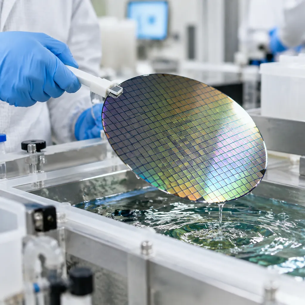
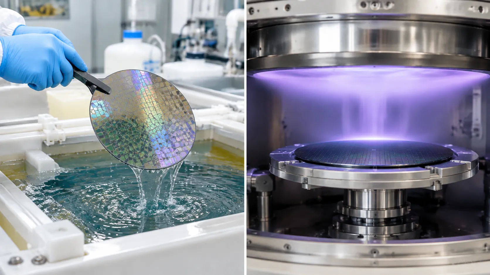
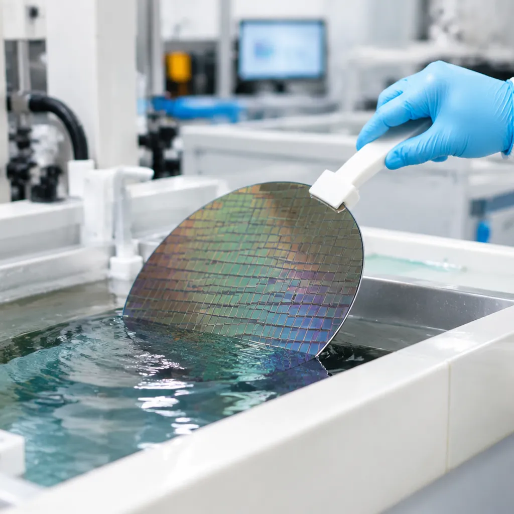
Liquid-phase chemical removal remains indispensable in modern cleanrooms for pattern definition, thin-film stripping, and surface conditioning.
Liquid-Phase Etching in FEOL, BEOL, and Advanced Packaging
We utilize wet chemical etching across every phase of wafer fabrication:
-
- Front-End of Line (FEOL): High-selectivity gate dielectric removal, pad oxide stripping, sacrificial oxide etching, and native oxide removal prior to thermal oxidation or epitaxy.
- Back-End of Line (BEOL): Metal interconnect patterning, barrier seed layer stripping, post-reactive-ion-etch (RIE) polymer cleaning, and defect reduction.
- Advanced Packaging & MEMS: Under-bump metallization (UBM) etching, substrate thinning, through-silicon via (TSV) cleaning, and bulk micromachining.
Wet Chemical Etching vs. Dry Plasma Etching
Selecting between wet and dry processes involves balancing profile fidelity against substrate selectivity and surface integrity:
| Process Metric | Semiconductor Wet Etch Process | Dry Plasma Etching (RIE / ICP) |
|---|---|---|
| Etch Rate Selectivity | Extremely High (often exceeding 100:1 for oxide-to-silicon or nitride-to-oxide) | Moderate to Low (selectivity constrained by physical ion bombardment) |
| Lattice Damage | Zero physical damage; purely chemical bond breaking preserves crystal integrity | Subsurface lattice damage, ion implantation, micro-roughness, and gate oxide charging |
| Profile Directionality | Predominantly isotropic; anisotropic along specific crystallographic planes | Highly anisotropic, vertical profiles optimized for dense sub-micron features |
| Throughput & CoO | High batch wafer processing capacity with a lower total cost of ownership | High capital cost, vacuum maintenance requirements, and single-wafer throughput limits |
Three-Step Reaction Kinetics
When wet etching semiconductor wafers, material removal depends on three sequential steps:
-
- Boundary Layer Diffusion: Fresh reactants diffuse from the bulk fluid across the stagnant hydrodynamic boundary layer to reach the wafer surface.
- Surface Chemical Reaction: The chemical etchant adsorbs onto the solid surface, initiates oxidation-reduction or complexation reactions, and breaks target bonds to form soluble reaction products.
- Byproduct Desorption: Soluble reaction byproducts desorb from the wafer surface and diffuse back across the boundary layer into the recirculated chemical stream.
Controlling Reaction Regimes in Wet Etching Semiconductor Fabrication
Maintaining tight critical dimension (CD) control requires identifying and controlling the rate-limiting step of the chemical mechanism:
- Reaction-Rate-Limited Regime:
- The surface reaction occurs slower than chemical mass transport.
- Etch rate is heavily dependent on bath temperature and activation energy.
- Yields uniform etching across complex topologies because fluid flow variations have minimal impact on material removal rates.
- Diffusion-Limited Regime:
- Mass transport across the boundary layer is slower than the surface reaction.
- Etch rate depends on bath velocity, flow distribution, and agitation intensity.
- Prone to pattern loading and non-uniformity between dense and open wafer areas without active boundary layer thinning.
We operate our processes primarily within the reaction-rate-limited regime by maintaining closed-loop bath temperature regulation while utilizing controlled chemical circulation to stabilize mass transfer dynamics.
Etching Profiles and Crystallographic Mechanics in Wafer Fabrication
Controlling etch directionality and profile geometry determines device performance in every semiconductor wet etch process. We categorize wet chemical removal into isotropic and anisotropic regimes based on how the chemical solution attacks the crystal lattice of the wafer.
Isotropic vs. Anisotropic Etch Profiles
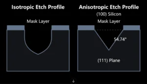
Isotropic Wet Etching Mechanics and Lateral Undercut
In isotropic etching, the liquid etchant dissolves material at equal rates in all spatial directions (spherical wavefront propagation).
-
- Etch Action: Non-directional chemical dissolution occurring vertically and horizontally underneath the protective mask.
- Lateral Undercut Calculation:
Lateral Undercut (δ) = Etch Depth (d) × (R_lat / R_vert)
(Where R_lat is the lateral etch rate and R_vert is the vertical etch rate. In a 100% isotropic system, R_lat / R_vert = 1, creating a 1:1 undercut-to-depth ratio). - Impact on Critical Dimension (CD): Lateral encroachment strips away pattern fidelity, making isotropic solutions suited primarily for blanket layer removal, pad oxide stripping, and non-critical geometry clearances in wet etching semiconductor fabrication.
Anisotropic Etching with KOH and TMAH
Anisotropic wet etching relies on orientation-dependent chemical reactions across single-crystal silicon planes:
| Parameter | Potassium Hydroxide (KOH) | Tetramethylammonium Hydroxide (TMAH) |
|---|---|---|
| Primary Plane Selectivity | (100) vs (111) up to 400:1 | (100) vs (111) up to 50:1 |
| CMOS Compatibility | No (Potassium ions cause mobile ionic contamination) | Yes (Metal-ion-free organic alkaline base) |
| Typical Concentration / Temp | 20–40 wt% at 70°C–90°C | 5–25 wt% at 70°C–85°C |
| Typical Applications | MEMS cavities, diaphragms, solar texturing | Front-end TSV tapering, IC cavity release |
-
- 54.74° Sidewall Formation: On a standard (100) silicon substrate, the dense atomic packing and stable back-bonds of the (111) crystallographic plane dramatically slow chemical dissolution. Etching self-terminates along these intersecting planes, yielding flat, highly predictable 54.74° angled sidewalls.
- Structure Alignment: Perfect alignment with wafer flat or notch axes prevents irregular stepped facets along the etched cavity walls.
Measuring Selectivity and Within-Wafer Non-Uniformity (WIWNU)
Precision wet processing requires tight statistical process control over selectivity and layer-to-layer uniformity across every lot:
-
- Etch Selectivity Ratio (S):
S = R_film / R_substrate (or R_film / R_mask)
High selectivity ensures complete film clearance without pitting, punch-through, or damaging underlying stops. - Within-Wafer Non-Uniformity (WIWNU):
WIWNU (%) = [(Max Etch Rate - Min Etch Rate) / (2 × Mean Etch Rate)] × 100
- Etch Selectivity Ratio (S):
Our automated systems, such as the wet etch tool semiconductor precision wafer etching system, utilize regulated flow dynamics and stable temperature control to keep WIWNU under 1.5% when wet etching semiconductor wafers across 150mm, 200mm, and 300mm manufacturing lines.
Essential Wet Etch Chemistries by Substrate and Film Layer
Matching the right chemical etchant to the target thin film dictates yield, profile control, and selectivity across every semiconductor wet etch process.
| Film / Layer | Target Chemistry | Operating Temp | Key Etch Mechanism & Function |
|---|---|---|---|
| Silicon Dioxide (SiO₂) | DHF (1:10 to 1:100) / BOE (6:1, 20:1) | 20°C – 25°C | Dissolution via fluoride ions; BOE maintains stable pH and steady etch rates |
| Silicon Nitride (Si₃N₄) | Hot Phosphoric Acid (H₃PO₄ 85%) | 150°C – 180°C | Hydrolysis of nitride bonds with high selectivity over SiO₂ and bulk Si |
| Bulk Silicon & Poly-Si | HNA (HF + HNO₃ + CH₃COOH) / KOH / TMAH | 20°C – 80°C | Redox dissolution (isotropic) or crystallographic plane etching (anisotropic) |
| Metal Layers (Al, Cu, UBM) | PAN etch / FeCl₃ / H₂O₂ mixtures | 25°C – 50°C | Controlled metal oxidation and chelation for interconnects and bump pads |
| Photoresist / Residue | Piranha (SPM: H₂SO₄ + H₂O₂) / RCA Cleans | 80°C – 130°C | Aggressive organic oxidation and post-etch surface particle removal |
Silicon Dioxide Etching Using HF Dips and BOE Systems
Standard hydrofluoric acid etching efficiently removes native oxides and thermally grown SiO₂ films via the net reaction:
SiO₂ + 6HF → H₂SiF₆ + 2H₂O
For critical oxide pattern definition, unbuffered HF depletes fluoride ions rapidly, causing fluctuating etch rates. We rely on buffered oxide etch (BOE / BHF)—a precise blend of ammonium fluoride (NH₄F) and HF. NH₄F acts as a buffering agent to replenish fluoride ions, maintain constant pH, and prevent photoresist peeling during critical wet etching semiconductor fabrication steps.
Silicon Nitride Stripping with Hot Phosphoric Acid
Removing silicon nitride (Si₃N₄) hard masks without attacking underlying pad oxides demands extreme etch rate selectivity. We utilize boiling phosphoric acid (H₃PO₄ at 85% concentration) maintained between 155°C and 165°C:
-
- Selectivity Control: Maintaining a controlled concentration of dissolved silicon (50–100 ppm) in the bath raises Si₃N₄:SiO₂ selectivity ratios beyond 50:1.
- Reflux & Spiking Systems: Boiling baths lose water rapidly, shifting acid concentration and boiling points. Automated DI water injection maintains boiling point stability and predictable nitride strip rates.
Bulk Silicon and Poly-Si Removal via HNA and Hydroxides
Etching poly-Si and monocrystalline silicon requires distinct chemical routes based on the target profile:
Isotropic HNA Solutions: A blend of Hydrofluoric, Nitric, and Acetic acids. Nitric acid (HNO₃) oxidizes silicon into SiO₂, HF dissolves the formed oxide, and acetic acid (CH₃COOH) buffers the reaction to prevent premature nitric decomposition.
Anisotropic Hydroxide Systems: Hot potassium hydroxide (KOH) and tetramethylammonium hydroxide (TMAH) selectively attack specific crystal lattices for trenching and MEMS structures. Our standalone wet process bench for semiconductor labs integrates closed-loop chemical controls to maintain tight bath stability during continuous hydroxide runs.
Metal Interconnect Etching for Aluminum, Copper, and UBM
Wet chemical etching provides fast, residue-free removal for back-end-of-line (BEOL) and packaging layers:
Aluminum Etch (PAN): A formulation of Phosphoric, Acetic, and Nitric acids heated to 40°C–50°C oxidizes and dissolves aluminum metallization traces smoothly.
Under-Bump Metallization (UBM) Stripping: Selective acid formulations strip sacrificial titanium (Ti), nickel (Ni), and gold (Au) seed layers around solder bumps without causing undercut or galvanic corrosion across adjacent pads.
Surface Preparation and Resist Stripping via Piranha and RCA Cleans
Chemical residue removal and surface passivation prepare wafers between etching phases:
Piranha Solution (SPM): A mixture of sulfuric acid (H₂SO₄) and hydrogen peroxide (H₂O₂) mixed at 3:1 to 5:1 ratios. Operating at 90°C–130°C through an exothermic reaction, SPM destroys heavy organic photoresist and polymerized sidewall residues.
RCA Standard Cleans: Standard Clean 1 (SC-1: NH₄OH / H₂O₂ / H₂O) dislodges organic contaminants and sub-micron particles, followed by Standard Clean 2 (SC-2: HCl / H₂O₂ / H₂O) to strip trace metallic ionic contamination from wet etching semiconductor wafers.
Process Bath Dynamics, Agitation, and Post-Etch Drying
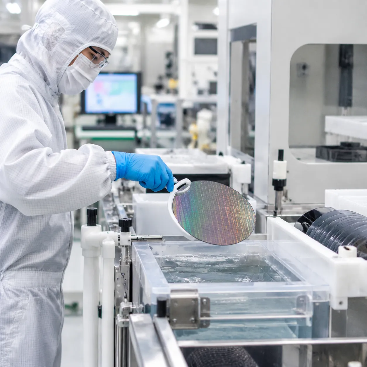
Inline Bath Concentration Tracking and Exothermic Control
Chemical consumption and evaporation alter bath kinetics over time, causing severe etch rate drift. To maintain consistent selectivity across continuous production runs, our systems apply closed-loop bath monitoring:
-
- Real-Time Inline Chemical Spiking: Automated dosing units measure concentration via refractive index, NIR spectroscopy, or conductivity, spiking raw chemicals (such as HF, H₂O₂, or NH₄OH) to maintain tight concentration margins.
- Active Exothermic Management: Aggressive acid-oxidizer mixtures generate substantial heat. Integrated fluoropolymer heat exchangers and dual-jacketed cooling loops regulate bath temperatures within ±0.5°C to avoid runaway etch rates.
- Continuous Recirculation & In-Line Filtration: High-purity pumps cycle the chemical etchant through fine-pore filtration loops, continuously removing suspended particles before the solution re-enters the process chamber.
Boundary Layer Thinning via Recirculation and Wafer Oscillation
During the processing of wet etching semiconductor wafers, stagnant chemical boundary layers at the substrate surface can throttle reaction rates and degrade within-wafer non-uniformity (WIWNU). We implement specialized fluid agitation inside our batch immersion wet bench systems for wafer processing to maximize mass transfer:
| Fluid Control Mechanism | Engineering Function | Impact on Wafer Yield |
|---|---|---|
| Continuous Weir Overflow | Four-sided overflow weir directing surface flow to filtration | Sweeps floating particles away and prevents surface re-deposition |
| Programmable Wafer Oscillation | Controlled vertical and horizontal mechanical movement | Thins diffusion boundary layers to enhance reactant exchange in deep trenches |
| Sub-Surface Injection Manifolds | Uniform bottom-up laminar fluid injection | Eliminates dead zones and delivers fresh chemistry across every wafer slot |
Megasonic Agitation for Sub-Micron Defect Removal
Sub-micron geometries frequently trap hydrogen gas bubbles and chemical byproducts within narrow aspect ratios. We integrate multi-frequency megasonic agitation (typically 700 kHz to 2 MHz) directly into our immersion tanks. The acoustic micro-streaming forces penetrate high-density patterns to dislodge microscopic particles and clear trapped gas without generating the violent cavitation pressures that cause fragile fin or gate pattern collapse.
Quick Dump Rinsing (QDR) and Marangoni IPA Vapor Drying
Terminating the chemical etch instantly and drying wafers without structural damage is critical for high yields:
-
- Quick Dump Rinsing (QDR): High-speed bottom dump valves evacuate the chemical rinse volume in under two seconds, coupled with top-mounted DI water spray nozzles to rapidly strip residual etchant and stop chemical action immediately.
- Marangoni IPA Vapor Drying: As the wafer carrier is slowly pulled from ultra-pure DI water, an isopropyl alcohol (IPA) vapor stream is introduced at the receding fluid meniscus. The difference in surface tension pulls water cleanly off the hydrophobic surfaces, providing watermark-free drying while preventing capillary stiction on high-aspect-ratio microstructures.
Equipment Architecture for Wet Etching Semiconductor Fabrication: Batch Wet Benches vs. Single-Wafer Tools
Selecting the right equipment architecture for your semiconductor wet etch process directly dictates defect density, chemical consumption, and overall wafer throughput. We balance these operational metrics by deploying two core tool configurations engineered specifically for wet etching semiconductor wafers: automated immersion wet benches and single-wafer spin processors.
Automated Immersion Wet Benches for High Throughput
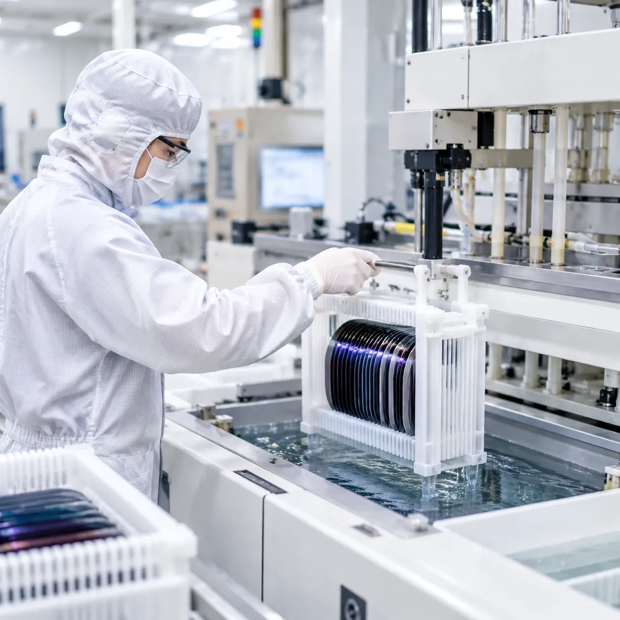
For high-volume manufacturing (HVM), automated batch immersion wet benches deliver unmatched wafer-per-hour output by processing entire wafer carriers (25 to 50 wafers) simultaneously across multi-tank chemical sequences.
Multi-Tank Process Flow: Sequential chemical etch, quick dump rinse (QDR), and advanced drying integrated into a continuous automated line.
Inline Chemical Spiking & Recirculation: Continuously filtered closed loops maintain steady bath concentration, bath life, and uniform etch rates across every lot.
We configure our high-precision wet benches for semiconductor processing with multi-axis robotics to eliminate wafer-handling shock and maximize lot-to-lot repeatability.
Single-Wafer Spin Processors for Critical 300mm Control
When sub-nanometer within-wafer non-uniformity (WIWNU), bevel cleaning, or backside etching is required, single-wafer architecture prevents cross-surface contamination and fluid stagnation.
Controlled Chemical Dispense: Localized nozzles apply fresh, temperature-controlled etchants to rotating wafers, eliminating boundary layer buildup.
Precision Bevel and Backside Etch: Protects active frontside topographies using inert gas cushions while stripping edge-bead polymers and unwanted metallic residues.
For tight-tolerance advanced nodes, our single-wafer wet processing equipment for 300mm fabs ensures exceptional surface symmetry without mechanical edge grip damage.
| Architecture Component | Construction Material | Target Process Application | Key Benefit |
|---|---|---|---|
| Acid Immersion Baths | Molded High-Purity PTFE / PFA | HF, BOE, SC-1, SC-2, and metal etchants | Total chemical inertness & ultra-low trace metal leach |
| High-Temp Baths | Fire-Polished Quartz | Hot Phosphoric Acid (H_3PO_4) for Si_3N_4 strip | Thermal shock resistance up to 180°C |
| Solvent Modules | 316L Stainless Steel / FM4910 | Solvents, photoresist stripping, surface prep | Static dissipation and fire-safe containment |
| Fluid Sealing | FFKM / High-Grade Fluoroelastomers | Inline valving, drain manifolds, and pump seals | Zero swelling and high MTBF in aggressive chemistries |
Chemical Segregation, Exhaust Integration, and Effluent Management
Maintaining process safety and fab compliance requires strict physical isolation between reactive chemistries:
Segregated Drains: Independent drainage manifolds keep fluorinated acids, heavy-metal-bearing effluents, organic solvents, and caustic baths completely separate to prevent hazardous cleanroom reactions.
Dynamic Exhaust Balancing: Real-time static pressure sensors modulate acid and solvent exhaust dampers, capturing toxic chemical fumes directly at the tank lip without destabilizing cleanroom laminar airflow.
Effluent Neutralization Integration: Continuous automated dosing systems neutralize spent acids and bases before disposal, ensuring cleanroom wastewater meets strict environmental thresholds.
Troubleshooting Semiconductor Wet Etch Process Defects and Yield Loss
Fixing Pattern Undercut, Photoresist Lifting, and Adhesion Failure
Excessive lateral etch attack and resist delamination degrade critical dimension (CD) control. When chemical etchants seep under masked features, pattern integrity fails.
-
- Root Causes: Inadequate substrate dehydration, degraded hexamethyldisilazane (HMDS) vapor prime, prolonged bath immersion beyond the etch endpoint, or aggressive isotropic chemical attack.
- Engineering Fixes:
- Re-optimize dehydration bakes (150°C) and HMDS deposition parameters prior to lithography to maximize surface hydrophobicity.
- Adjust etchant dilution or convert to buffered chemistries to reduce aggressive lateral attack rates.
- Implement strict endpoint detection to prevent over-etching and limit critical dimension (CD) bias.
| Defect Type | Primary Mechanism | Corrective Fab Action |
|---|---|---|
| Resist Lifting | Poor interfacial adhesion / chemical penetration | Optimize HMDS priming & post-exposure bake (PEB) |
| Severe Undercut | Over-etching / unbuffered chemical attack | Tighten bath timing; switch to buffered systems (e.g., BOE) |
| Micromasking | Insoluble residues / native oxide patches | Pre-etch dilute acid dip & tank surfactant dosing |
| Galvanic Pitting | Electrochemical potential mismatch at metal junctions | Adjust bath pH, add corrosion inhibitors, minimize light exposure |
Eliminating Micromasking, Native Oxide Residue, and Trapped Hydrogen Bubbles
During wet etching semiconductor wafers, localized masking blocks fresh chemical contact, leaving unetched pillars, pyramids, or irregular grass-like defects across the wafer surface.
-
- Hydrogen Bubble Entrapment: Redox reactions (such as silicon or metal dissolution) generate gaseous byproducts like $H_2$. If bubbles cling to the surface, they block etchant flow and create circular unetched voids. We solve this by adding fluorosurfactants to lower surface tension and applying synchronized fluid displacement across the tank weir.
- Native Oxide and Organic Residues: Incomplete pre-cleaning leaves patchy oxide layers that cause uneven etch initiation. Running an integrated dilute HF pre-dip immediately before the main etch clears native films and guarantees uniform surface wetting.
Mitigating Surface Roughness, Pinholes, and Micro-Galvanic Corrosion
Target film removal must leave pristine, defect-free underlying interfaces. Rough surfaces and pitting compromise subsequent deposition steps.
-
- Thermal and Mass-Transport Uniformity: Localized temperature spikes accelerate reaction rates unpredictably. Precision inline heaters maintain bath temperature stability within ±0.5 °C across our wet bench chemistry equipment to prevent thermal runaways and surface pitting.
- Galvanic Attack Prevention: When dissimilar metals interface in conductive chemical baths (e.g., Al-Cu lines or under-bump metallization), bimetallic corrosion can rapidly dissolve the more active metal. Adding corrosion inhibitors and controlling bath redox potential suppresses this galvanic reaction.
Bath Filtration Optimization Using Sub-0.02 Micron PTFE Filters
Recirculating particulate matter is a primary cause of micro-defects and line bridging. Effective contamination control demands robust physical filtration integrated into chemical circulation loops.
-
- Membrane Selection: We utilize fully fluoropolymer, sub-0.02 micron PTFE filter cartridges rated for high chemical compatibility with aggressive acids, oxidizers, and solvents.
- Turnover Rates: Maintaining tank recirculation turnover rates of at least 2 to 3 bath volumes per minute ensures continuous capture of precipitated salts and sheared resist flakes before they resettle on wafer surfaces.
- Proactive Maintenance: Monitoring differential pressure ($\Delta P$) across filter housings prevents filter breakthrough. Regularly servicing fluid lines and stocking recommended wet bench spare parts to minimize downtime ensures chemical baths stay within strict class-1 cleanroom particle baselines.
Wet Etching vs. Dry Plasma Etching Fab Decision Matrix
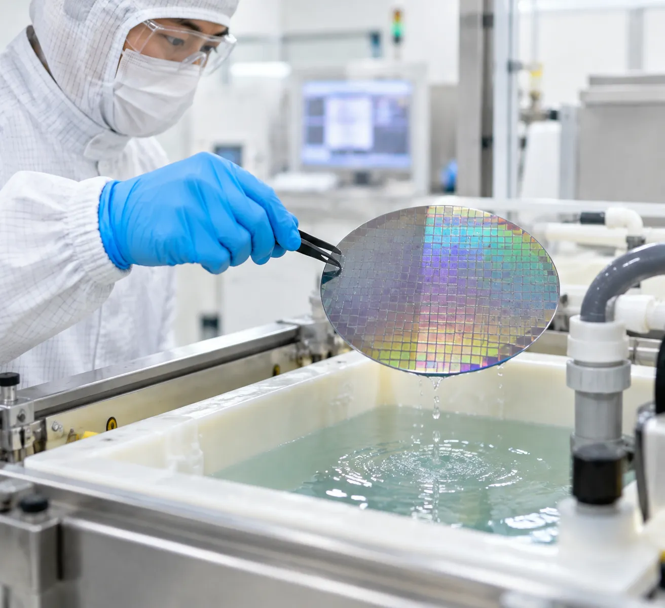
Choosing between liquid-phase chemical removal and reactive plasma steps directly defines device performance, defect margins, and production line capital expense. When configuring a semiconductor wet etch process alongside dry etching modules, we weigh profile control against chemical selectivity and substrate surface damage.
| Metric | Wet Chemical Etching | Dry Plasma Etching (RIE / ICP) |
|---|---|---|
| Profile Directionality | Primarily isotropic (crystallographic anisotropic for select substrates) | Highly anisotropic (directional ion bombardment) |
| Selectivity Margin | Exceptionally high (>100:1 typical) | Moderate to low (often <20:1) |
| Substrate Lattice State | Zero physical or crystal damage | Surface lattice damage and charge |
| Cost of Ownership (CoO) | Low tooling and consumable overhead | High capital, vacuum, and gas expense |
| Wafer Throughput | High batch immersion capacity | Limited to single-wafer or low batch |
Directionality, Selectivity Margins, and Aspect Ratios
In advanced wet etching semiconductor fabrication, chemical baths provide unmatched material selectivity margins that dry plasma cannot reach without eroding underlying mask layers. While dry etching excels at cutting deep, vertical trenches with tight aspect ratios, wet chemical solutions dissolve target layers cleanly right down to the interface stop layer without attacking adjacent features.
-
- Etch Profile Control: Wet chemistries deliver uniform lateral removal under mask layers, ideal for broad isotropic clearing, planarization, and crystallographic groove formation on a silicon substrate.
- Selectivity Ratios: Liquid etchants routinely deliver film-to-substrate selectivity ratios exceeding 100:1, eliminating critical thin-film punch-through risks during gate and dielectric layer stripping.
- Aspect Ratio Limits: High-aspect-ratio sub-micron features face surface tension and mass transport limitations in liquid baths, making dry plasma the preferred choice for deep vertical contacts and isolation trenches.
Substrate Damage Risks: Chemical Dissolution vs. Ion Bombardment
Physical ion bombardment in reactive ion etching (RIE) frequently causes micro-roughness, crystal lattice dislocation, and trapped charge accumulation. In contrast, wet etching semiconductor wafers relies purely on chemical dissolution kinetics:
-
- Lattice Integrity: Liquid reactions selectively consume surface bonds without transferring physical kinetic momentum, completely preserving the underlying crystal structure.
- Gate Oxide Protection: Eliminating RF plasma fields prevents thin dielectric breakdown caused by antenna-effect charge buildup.
- Residue-Free Interfaces: Chemical baths neutralize and dissolve contamination layers without baking fluorocarbon polymer residues onto sidewalls.
Cost of Ownership (CoO), Chemical Consumption, and Throughput
From an operational standpoint, wet processing maintains a significantly lower cost of ownership (CoO) per wafer. Wet etching stations eliminate high-maintenance vacuum pumps, turbo molecular stages, and expensive RF generator power supplies.
-
- Batch Capacity: Multi-wafer immersion tanks process 25 to 50 wafers simultaneously, delivering far higher hourly throughput than single-wafer vacuum chambers.
- Chemical Management: Automated chemical replenishment and spiked bath extensions minimize raw chemical consumption. When planning fab tool capacity, reviewing a standardized wet bench selection guide helps balance bath life, bath heating demands, and exhaust infrastructure.
Process Window Selection: Sub-Micron Nodes vs. Legacy Technologies
We balance wet and dry steps across the integration flow based on node scaling and structural tolerance:
-
- Sub-Micron and Advanced Nodes (<28nm): Reserved for selective sacrificial layer release, gate oxide pre-cleans, unmasked backside thinning, and damage-free hardmask removal where plasma would punch through ultra-thin active junctions.
- Legacy Nodes, Power Devices, and MEMS (>90nm): Primary method for pad oxide etching, bulk micromachining, wafer thinning, emitter patterning, and under-bump metallization (UBM) stack clearing, where high throughput and low tooling cost govern overall fab profitability.
Advanced Trends in Semiconductor Wet Processing
As device geometries shrink below 3nm and power electronics migrate to wide-bandgap substrates, the semiconductor wet etch process is evolving beyond bulk material removal into atomic-level surface engineering. Modern fabs rely on cutting-edge chemical selectivity and eco-efficient wet stations to handle complex 3D architectures and resilient crystal lattices.
Atomic-Scale Selective Etching for GAA-FET Nanosheets
In Gate-All-Around (GAA-FET) and multi-bridge channel architectures, releasing horizontal silicon nanosheets requires removing sacrificial silicon-germanium (SiGe) layers without degrading adjacent silicon channels.
-
- Hyper-Selective Chemistries: We utilize specialized oxidizer-acid mixtures (such as modified HF/H2O2/CH3COOH solutions) that achieve isotropic SiGe:Si selectivity ratios exceeding 150:1.
- Surface Uniformity: Maintaining a consistent chemical boundary layer across dense nanosheet stacks avoids channel stiction, lateral pinch-off, and non-uniform channel dimensions.
- Zero Crystal Damage: Unlike reactive ion etching, precision wet chemistry clears tight sub-10nm gaps without introducing lattice defects or plasma-induced charging damage.
GAA Nanosheet Selective Release
[ Si Channel ]
[ SiGe Sacrificial ] → [ Selective Wet Etch ] → Cavity Formed
[ Si Channel ]
Wet Chemical Etching for Wide-Bandgap SiC and GaN
Compound semiconductors like Silicon Carbide (SiC) and Gallium Nitride (GaN) feature strong chemical bond energies that resist standard room-temperature acids. Adapting wet etching semiconductor wafers made of wide-bandgap materials requires specialized processing techniques:
| Substrate Material | Primary Etch Mechanism | Key Chemical Formulations | Critical Fab Application |
|---|---|---|---|
| Silicon Carbide (SiC) | Molten salt dissolution & defect-selective etching | Molten KOH / $KNO_3$ (450°C–600°C) | Defect delineation and surface micropipe decoration |
| Gallium Nitride (GaN) | Photo-Electrochemical (PEC) oxidation-dissolution | $H_2SO_4 / H_2O_2$ or KOH under UV illumination | Mesa isolation, LED patterning, and high-electron-mobility transistor (HEMT) processing |
| Gallium Arsenide (GaAs) | Redox kinetic etching | Citric acid / $H_2O_2$ / $H_2O$ systems | Optoelectronic facet definition and selective buffer removal |
Sustainable Cleanroom Initiatives and Green Chemistries
Modern fabs must balance high throughput with sustainability. Upgrading legacy chemical stations into eco-friendly setups directly lowers the cost of ownership and meets strict environmental cleanroom standards:
-
- Closed-Loop Chemical Recycling: Automated inline concentration monitoring dynamically blends and spikes baths, extending the chemical bath life of hydrofluoric and sulfuric mixtures by up to 300%.
- Green Stripping Alternatives: Replacing toxic solvents like NMP (N-Methyl-2-pyrrolidone) with biodegradable, water-soluble organic strippers delivers clean photoresist lift-off without hazardous VOC emissions.
- Exhaust & Effluent Treatment: Integrating our advanced wet processing tools directly with high-efficiency chemical exhaust scrubbers neutralizes volatile acid fumes at the point of use.
- Micro-Volume Dispensing: Transitioning specialized steps to single-wafer chambers dramatically cuts wet chemical consumption across high-volume 300mm wafer fabrication lines.
Understanding these next-generation chemical mechanisms ensures your fab maximizes yield on cutting-edge nodes. Explore our engineering guides in the wet process basics knowledge center to optimize bath kinetics and chemical compatibility across your production floor.
Frequently Asked Questions About Semiconductor Wet Etching
What is the Difference Between Isotropic and Anisotropic Wet Etching?
The primary difference lies in directional etch mechanics and profile control during the semiconductor wet etch process:
-
- Isotropic Etching: Proceeds at an equal rate in all spatial directions. It leads to lateral undercut beneath the masking layer, which is ideal for non-critical oxide stripping, isotropic pad removal, and sacrificial layer release.
- Anisotropic Etching: Exhibits orientation-dependent etch rates along specific crystal lattice planes. Using alkaline solutions like potassium hydroxide (KOH) or tetramethylammonium hydroxide (TMAH) on silicon substrates, anisotropic etching yields distinct geometric sidewalls (such as 54.74° angles on <100> silicon) for MEMS structures and deep cavities.
| Parameter | Isotropic Wet Etching | Anisotropic Wet Etching |
|---|---|---|
| Etch Rate Directionality | Equal in all directions ($x, y, z$) | Crystallographic plane-dependent |
| Typical Chemistries | HF, BOE, HNA mixtures | KOH, TMAH, EDP |
| Profile Shape | Rounded, lateral undercut | Sloped sidewalls, precise geometric pits |
| Primary Fab Uses | Oxide dips, isotropic strip, cleaning | MEMS diaphragms, trenches, TSV cavities |
Why is Buffered Oxide Etch Preferred Over Standard Hydrofluoric Acid?
Standard hydrofluoric acid (HF) dips rapidly deplete active fluoride ions during silicon dioxide ($SiO_2$) removal. This depletion alters the chemical bath pH, resulting in drifting etch rates and poor Within-Wafer Non-Uniformity (WIWNU).
Buffered Oxide Etch (BOE / BHF) combines HF with a buffering agent—typically ammonium fluoride ($NH_4F$) in ratios like 6:1 or 10:1. This formulation delivers distinct advantages:
Stable Fluoride Ion Concentration: Maintains a constant chemical activity and predictable etch rate throughout bath life.
pH Stabilization: Minimizes photoresist attack, preventing mask peeling and excessive critical dimension (CD) bias.
Consistent Etch Rate Selectivity: Delivers tight control over thin dielectric layers without damaging underlying silicon.
How Does Megasonic Agitation Improve Wet Etching Uniformity?
During wet etching semiconductor fabrication, static chemical baths create a stagnant hydrodynamic boundary layer on the wafer surface that slows mass transport. Integrating megasonic agitation (0.8 to 2 MHz) directly addresses this bottleneck:
Boundary Layer Thinning: High-frequency acoustic streaming thins the fluid boundary layer, accelerating chemical replenishment and byproduct desorption.
Defect-Free Particle Removal: Cavitation forces dislodge sub-micron particles and native micro-bubbles without damaging fragile, high-aspect-ratio structures.
Enhanced Cavity Wetting: Forces active chemical etchants into high-density contact holes and deep trench networks for uniform chemical exposure.
What Causes Wafer Stiction During the Drying Phase and How is it Resolved?
Wafer stiction occurs when surface tension from evaporating rinse water creates capillary forces strong enough to pull adjacent microstructures together, causing permanent mechanical collapse.
We eliminate stiction and watermark defects by integrating Marangoni IPA vapor drying and surface tension reduction protocols into our advanced wet process technology. Introducing isopropyl alcohol (IPA) vapor creates a surface tension gradient across the receding DI water meniscus. This gradient pulls liquid cleanly off the substrate without leaving capillary bridges or drying residues.
When Should a Fab Choose Single-Wafer Processing Over a Batch Wet Bench?
Tool selection depends on wafer geometry, throughput targets, defect margins, and chemical segregation requirements:
-
- Batch Immersion Wet Benches: Best suited for high-volume manufacturing, bulk photoresist stripping (Piranha/SPM), standard RCA cleans, and non-critical oxide dips where maximizing wafers-per-hour (WPH) reduces overall cost of ownership.
- Single-Wafer Spin Processors: Essential for advanced nodes (sub-28nm) and 300mm wafer lines requiring single-side processing, wafer backside etching, precise bevel cleaning, and zero cross-contamination risk.
For specialized lines and high-mix environments, deploying modular custom wet process stations allows process engineers to balance high throughput with recipe flexibility across varying substrate materials.